Also at ]Department of Electrical and Computer Engineering, University of Rochester, Rochester, New-York, 14627
Spin transport theory in ferromagnet/semiconductor systems with non-collinear magnetization configurations
Abstract
We present a comprehensive theory of spin transport in a non-degenerate semiconductor that is in contact with multiple ferromagnetic terminals. The spin dynamics in the semiconductor is studied during a perturbation of a general, non-collinear magnetization configuration and a method is shown to identify the various configurations from current signals. The conventional Landauer-Büttiker description for spin transport across Schottky contacts is generalized by the use of a non-linearized I-V relation, and it is extended by taking into account non-coherent transport mechanisms. The theory is used to analyze a three terminal lateral structure where a significant difference in the spin accumulation profile is found when comparing the results of this model with the conventional model.
I Introduction
Hybrid semiconductor/ferromagnet material systems play a key role in spintronics research Zutic_RMP04 . The motivation to study these systems is twofold. First, computing technologies rely on the ability to easily tune the carrier density in semiconductors. Second, the advances in storage applications rely on the ability to inject or extract spin polarized electrons across interfaces between non-magnetic and ferromagnetic materials Johnson_Silsbee_PRB87 -Prinz_Science98 . In the last decade, spin injection from ferromagnetic materials into semiconductors has been showing a significant progress Zhu_PRL01 -Appelbaum_PRL07 together with a better understanding of the interface transport properties Butler_JAP97 -Honda_PRB08 . This progress has been accompanied with theoretical analysis of basic spin transport phenomena starting with the conductivity mismatch between a magnetic metal and a semiconductor Johnson_Silsbee_PRB87 ; Schmidt_PRB00 ; Rashba_PRB00 ; Fert_PRB01 ; Smith_PRB01 , and continuing with effects of electrical fields Yu_Flatte_long_PRB02 ; Albrecht_PRB03 , of lateral transport Dery_lateral_PRB06 , and of time dependent response Rashba APL02 ; Cywinski_APL06 ; Dery_Nature07 . In this paper we provide a comprehensive theory of time-dependent spin transport in semiconductor/ferromagnet (SC/FM) systems. It studies the potential and spin accumulation profiles in a general non-collinear setup of magnetization directions. Two new aspects are provided in deriving the transport equations. First, we elaborate on the quasi-neutrality approximation that simplifies the description of the drift diffusion equations. We show that the reasoning for this often-invoked approximation is different than what has been assumed since the late 1940’s Shockley_BSTJ49 -Roosbroeck_PR61 . Second, we take into consideration the localization of electrons due to the doping inhomogeneity of typical SC/FM junctions Hanbicki_APL02 ; Jonker_IEEE03 ; Adelmann_JVST05 . This leads to a change of the canonical boundary conditions that rely on the Landauer-Büttiker formalism Schmidt_PRB00 -Dery_Nature07 . We use this model to analyze lateral geometries which capture the vast majority of spin injection experiments Johnson_Science93 -Crooker_PRB09 . The analysis considers the intrinsic capacitance of the SC/FM contacts and the two-dimensional profiles of the electrical field and spin accumulation Cywinski_APL06 ; Dery_Nature07 .
This paper is organized as follows. Sec. II presents a time dependent analysis of spin transport in a bulk semiconductor region and across a SC/FM junction. Sec. III discusses the modifications that should be introduced in realistic systems. It deals with the revision of the boundary conditions in forward biased junctions and with their voltage bias limitations. In Sec. IV we apply our model to a non-collinear, three terminal planar geometry and we quantify the time dependent readout across a capacitive barrier. Sec. V provides a summary. Descriptions of technical numerical procedures are provided in separate appendices.
II General Formalism
Theoretical analysis of spin injection from metals into semiconductors shows that non-ohmic junctions are necessary for the current to be polarized Johnson_Silsbee_PRB87 ; Schmidt_PRB00 ; Rashba_PRB00 ; Fert_PRB01 ; Smith_PRB01 . More precisely, since the spin-depth conductance of the semiconductor (conductivity divided by spin-diffusion length) is much smaller than its metal counterpart, for spin injection to occur the junction conductance has to be similar or smaller than the semiconductor spin-depth conductance. This spin injection constraint is easily achieved by an insulator barrier or by the naturally formed Schottky barrier at the interface between a metal and a semiconductor Tunneling_Phenomena ; Sze . In the case of a thin tunneling barrier, the electrochemical potential is discontinuous at the junction and as a result, the spin polarization of the current is driven solely by the spin selective transmission across the junction. The much larger conductivity and spin-depth conductance in the ferromagnet render the spatial and spin dependence of its potential level negligible. Thus, in the following we describe the spin transport only in the bulk semiconductor region and across the SC/FM junction whereas the ferromagnet is considered as a reservoir with a uniform potential level. We investigate in detail lateral systems that consists of ferromagnetic contacts on top of a non-degenerate semiconductor channel. When applicable, we rely on previous theoretical investigations of spin-transport in metals. These include both time dependent Zhang_PRB02 -Zhu_PRB08 and non-collinear Slonczewski_PRB89 -Xu_Nanotechnology08 aspects. In our analysis, we do not consider the effects of ballistic transport Brataas_PRL00 , of external magnetic fields Hernando_PRB00 , or of anisotropic spin relaxation Saikin_JPCM04 .
II.1 Bulk Semiconductor
Macroscopic transport equations describe particle conservation and current processes. These equations can be derived from the zeroth and first moments of the dynamical Boltzmann transport equation Valet_PRB93 and they provide a spatial and temporal connection between spin dependent electron and current densities ( & ). The accumulated (depleted) spin population at is directed in the () direction. Using the relaxation time approximation, these derived transport equations are given by,
| (1) | |||||
| (2) |
where the indices & denote either or . is the elementary charge and is the macroscopic electric field. The spin-dependent macroscopic parameters are the spin-flip time from spin to spin and vice versa ( & ), the diffusion coefficients (), the conductivities () and the momentum relaxation times (). The current terms are eliminated by substituting the continuity equation into the divergence of the current equation,
| (3) | |||
At this phase, one can derive the dynamical spin dependent drift-diffusion equation by applying a series of controlled approximations after which the first line is rewritten in a more compact form and the second line (curly brackets) is neglected Schmidt_PRB00 -Dery_Nature07 . In non-degenerate and homogeneous semiconductors, the diffusion constant and momentum relaxation time are spin and position independent: == & ==. In addition, the spin-flip times are equal and much greater than the momentum relaxation time, == . We can therefore accurately approximate the above equation as,
| (4) |
where denotes the mobility (). Zhu et al. have studied the wave-like behavior due to the second order time derivative in magnetic metallic systems (vanishing terms) Zhu_PRB08 . They have shown that this effect becomes significant at time scales shorter than . On the other hand, if the interest is in semiconductors and in much longer time scales then a different approach is needed. First, we define the spin polarization along the axis and the charge accumulation,
| (5) |
denotes the electron density in the conduction band due to the background doping. Taking into account the Poisson equation as well as the difference and sum of Eq. (4) with its corresponding equation () one gets,
| (6) | |||||
| (7) | |||||
| (8) |
is the dielectric relaxation time defined by the ratio between the static dielectric constant and the total conductivity, , where . The plasma frequency is defined by where is the effective mass of the electron in the semiconductor. Since in most cases the interest is in time scales much longer than the momentum relaxation time, it is common to neglect the wave-like behavior already when describing the current components (=0 in Eq. (2)). The resulting charge dynamics is then described by a diffusion equation which in the linear regime of small charge perturbations reads . The argument for invoking the quasi-neutrality approximation is then that any local charge imbalance () is being screened out within a time scale of the order of . This is a widely used argument, whose origin can be traced back to the seminal works on bipolar transport in homogeneous semiconductors Shockley_BSTJ49 -Roosbroeck_PR61 . However, by keeping the wave-like terms then the decay of is actually governed by and it is nearly independent of . This is a manifestation of the finite propagation velocity which also results in an oscillatory behavior during the relaxation. It is still justifies, however, to assign =0 in Eqs. (6) and (8) but the argument should refer to interest in time scales much longer than . This statement is general and should not change qualitatively if the original transport equations ((1) & (2)) are derived without employing the relaxation-time approximation. Moreover, the exclusion of spin dependent parameters in Eqs. (7) and (8) also suggests that the charge dynamics is general. For example, similar charge dynamics describes bipolar transport in homogeneous semiconductors. The charge accumulation is then due to deviation of hole and electron densities from their local equilibrium, . In a different publication we will revisit the widely used quasi-neutrality concept, and elucidate the true nature of ultra-fast charge dynamics in various systems Yang_neutrality . Here, we provide an example that investigates the applicability of the adiabatic approximations () in deriving the spin dependent transport equations in semiconductors. One should recall, however, that this classical approach (Eqs. (7) & (8)) neglects the effect of dynamical screening. At relatively low electron densities (e.g., non-degenerate semiconductors) this classical description is accurate since the screening length is larger or comparable to the mean free path.
We study the charge accumulation evolution after a disturbance that locally breaks the charge neutrality in an overall neutral bulk semiconductor. The charge current density at the boundaries of the system is at all times. The dynamical response is similar for all systems in which the external electric field is negligible compared with the initial built-in electric field due to the charge imbalance ( is smaller than some critical current density). For simplicity the analysis proceeds with . We assume the disturbance happens far from the system boundaries and that it is spherically symmetric. Based on these conditions, the charge evolution and the electric field possess a spherical symmetry. We choose a representative initial charge profile due to the disturbance, . is a constant chosen to keep the integrated space charge zero and reflects the initial intensity of the disturbance at the center. The spatial extent of the disturbance is determined by . For the second needed initial information we set (this choice does not qualitatively change the following discussion).
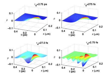
Fig. 1 shows the evolution of a charge disturbance whose peak intensity is and its spatial extent is =60 nm. We consider a room temperature, non-degenerate n-type GaAs with a momentum relaxation time of fs. The resulting mobility and diffusion constant are, respectively, 2600 cm2/Vs and 68 cm2/s. Panels (a)-(d) show, respectively, the evolution with these parameters for doping densities of cm-3. The resulted dielectric relaxation time is changed over three orders of magnitude (). In spite of the large changes in , the decay time is about 2=200 fs in all cases. The exp decay is a universal behavior if Yang_neutrality . The results also show a clear oscillatory behavior at shorter dielectric relaxation times where the oscillation frequency matches the plasma frequency, . To understand this behavior we consider the Fourier transform of the initial disturbance. Its effective width is and its coherence time scale is defined by . If the initial disturbance is relatively wide such that, , then the oscillations are governed by the (central) plasma frequency. The oscillatory behavior is damped when due to the destructive interference between the wavevector components of the disturbance. Studying these and other effects (e.g., the role of momentum relaxation time, the non-linear terms, confined and open systems) are beyond the scope of this paper and will be studied elsewhere Yang_neutrality .
To summarize the quasi-neutrality aspect, if the interest is in spin phenomena at time scales much longer than (and not ), then it is accurate to apply the adiabatic approximations (), and get a divergence-free electric field and a linear dynamical spin-drift-diffusion equation,
| (9) | |||||
| (10) |
where is the spin-diffusion length and the Einstein relation was invoked, .
The spin dependent electrochemical potential, , is also an important transport quantity which has the following relation with ,
| (11) |
where denotes the spin independent part defined by the sum of a constant chemical potential and the electrical potential. The latter is driven by the applied bias voltage and is related to the electrical field via . The logarithmic term refers to the non-degenerate case (with ).
To this point, we have treated the spin polarization in the channel, , as a scalar which implicitly relies on the assumption that the net spin has a fixed direction throughout the semiconductor channel. This description is valid in collinear systems at which the magnetization directions in all of the ferromagnetic elements share a common (easy) axis. In a more general, non-collinear configuration the boundary conditions impose a change in the direction of the spin polarization during the transport in the channel. For a general coordinate system in spin space, the spin dependent electron density is described by a x matrix,
| (12) |
where is the Pauli matrix vector and has the magnitude along the direction as defined in Eq. (5). Using this notation and repeating the analysis, the components of the spin-drift-diffusion equation read,
| (13) |
where () enumerates the , and coordinates in spin (real) space. According to Eq. (2), the components of the charge current density (vector) and of the spin current density (second-rank tensor) are,
| (14) | |||||
| (15) |
These expressions are valid if the frequency of the applied electrical signal is much smaller than .
II.2 SC/FM Junction
The description of transport is complete when the spin polarized currents across the SC/FM junctions are expressed in terms of the spin polarization vector at the semiconductor side of the junction, . We follow the notation by Brataas et al. Brataas_PRL00 ; Brataas_EPJB01 , and use Eqs. (11) & (12) to write the population distribution matrices on both sides of the junction,
| (16) | |||||
| (17) |
where denotes the energy. As mentioned before, due to the conductivity mismatch the ferromagnetic side is a reservoir with a constant chemical potential, , where (Eq.(11)) is evaluated at the semiconductor side of the junction and is the voltage drop across the SC/FM junction. () denotes forward (reverse) bias voltage in which electrons flow into (from) the ferromagnetic contact. For compact notation, the boundary conditions of each SC/FM junction are written in a spin coordinate system at which the -axis is collinear with the majority spin direction of the corresponding ferromagnetic contact. With this simplification, the reflection matrices are diagonal,
| (22) |
The reflection coefficients in the left (right) matrix are of electrons from the semiconductor (ferromagnetic) side of the junction. For a given material system, these coefficients vary with the voltage drop and with the longitudinal energy, , which denotes the impinging energy of electrons due to their motion toward the SC/FM interface. The up and down arrows denote, respectively, the majority and minority spin directions in the ferromagnetic contact where we have set the direction parallel to the majority direction. By using the Landauer-Büttiker formalism, the tunneling current density across the SC/FM junction is given by Brataas_PRL00 ; Brataas_EPJB01 ; Ciuti_PRL02 ,
The first (second) term in square brackets is related to the transmitted current from the ferromagnet (semiconductor) due to electrons whose total and longitudinal energies are and , respectively. The zero energy refers to the bottom of the semiconductor conduction band. The inner integration is carried over transverse wavevectors due to a motion in parallel to the SC/FM interface and its upper integration limit, , denotes the wavevector amplitude of an electron with energy . In the chosen spin coordinate system, the transmitted spin current from the ferromagnetic side is non-zero only along the direction. Its spin-up and spin-down components are proportional, respectively, to () and (), where we have rendered the fact that . The transmitted current from the semiconductor side, on the other hand, includes off-diagonal mixed terms that are proportional to . This is the case when due to the flow of electrons from/into ferromagnetic contacts which has non-collinear magnetization directions and that are located within about a spin-diffusion length. By substituting Eqs. (16)-(22) into Eq. (II.2) we write the energy resolved tunneling current density matrix,
| (26) | |||||
| (29) |
The components of the spin polarization vector are evaluated at the semiconductor side of the junction, and the direct and mixing conductances (per unit area) are given by,
| (30) | |||||
| (31) |
In this writing, the dependence of the reflection coefficients is resolved from & . The analysis is further simplified if we assume that the potential level in the ferromagnetic contact lies beneath the edge of the semiconductor conduction band, . Since in a non-degenerate semiconductor , this assumption holds for any forward bias conditions and for relatively low reverse bias conditions. Thus, we can consider only the Boltzmann tail of the ferromagnetic Fermi-Dirac distribution (first term in Eq. (26)). In this regime, the components of the tunneling current density across the SC/FM boundaries are compactly described by,
| (32) | ||||
| (33) | ||||
| (34) | ||||
| (35) |
The subscript is a real space coordinate directed along the normal of the SC/FM interface. The total and mixing macroscopic conductances ( & ) and the finesse () of the junction are given by,
| (36) | |||||
The reflection coefficients that appear in the boundary currents can be either extracted from carefully designed experiments Kawakami_Science01 ; Epstein_PRB02 ; Li_PRL08 , or calculated by various techniques. In this paper, we use an effective mass single band model Ciuti_PRL02 , Osipov_PRB04 -Smith_PRB08 . Details of the calculation are given in Appendix A. We mention that this model does not include the predicted effects of Ab-initio calculations Butler_JAP97 -Honda_PRB08 . These effects may become crucial in ideal SC/FM interfaces and concern spin-filtering mechanisms or the presence of interfacial bands.
III Realistic Modeling
There are several restrictions and mechanisms that should be considered in a realistic modeling of spin transport in biased SC/FM hybrid systems. The use of Poisson and linear spin-drift-diffusion equations ((9) & (13)) inside the homogenous bulk semiconductor is a reliable macroscopic description as long as ballistic effects are not important. However, three crucial aspects about the boundary currents need to be addressed. The first relates to the inhomogeneous doping profile at the Schottky barrier and it results in a change of the boundary conditions. The second aspect relates to the bias voltage across SC/FM junctions and it limits the applicability of the boundary conditions to a finite bias voltage range. The third relates to the intrinsic capacitance of the Schottky barriers and it plays a role in the dynamics.
III.1 Inhomogeneous doping profile
At low bias voltages, the width of the barrier should be about or less than 10 nm in order to suppress thermionic currents at room temperature (see Appendix A). Therefore, the doping concentration at the Schottky junction should be highly degenerate, 1018 cm-3. If the bulk of the semiconductor is non-degenerate (1018 cm-3) then the result is a strongly inhomogeneous doping profile between these regions Hanbicki_APL02 ; Jonker_IEEE03 ; Adelmann_JVST05 . The need for a much lower carrier density in the bulk region, stems from the condition of optimal spin accumulation density: the barrier conductance is of the same order of magnitude as the semiconductor spin-depth conductance Fert_PRB01 ; Dery_lateral_PRB06 . Since is relatively small even with a 10 nm wide barrier, the optimal ‘spin-impedance’ condition can be met with a bulk region that is moderately doped (low ) for which the spin-diffusion length, , is relatively large. Thus, for the spin accumulation density to be non-negligible the background doping densities are typically such that cm-3. As a result of the doping inhomogeneity between the bulk and the barrier regions, a potential well is likely to be created between these regions Zachau_SSC86 -Shashkin_Semiconductors02 . Even with a careful doping design at which there is no well in equilibrium, at forward bias when less electrons need to be depleted from the semiconductor, the well creation is inevitable. The spin related effects in this potential well may contribute to the spin accumulation in the bulk semiconductor region Dery_PRL07 ; Li_APL09 .
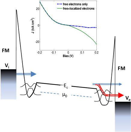
Fig. 2 shows the conduction band profile across a one-dimensional biased system (calculation details in Appendix A). The left and right barriers denote, respectively, the reverse (spin injection) and forward (spin extraction) biased junctions. Across the reverse biased junction, most of the injected hot electrons overshoot this region (although their reflection coefficients are slight modified by the potential well). On the other hand, in the forward direction, we should consider a new transport mechanism which involves the escape of spin polarized electrons from the potential well into the ferromagnetic contact. This process accompanies the previous mentioned process of free electrons tunneling (Eq. (II.2)). Therefore, free electrons from the bulk semiconductor region can either tunnel directly into the ferromagnetic metal or feed the potential well when its localized electrons escape. To quantify the spin dependent currents that flow to the potential well, we consider three mechanisms. The first is the capture time of a free electron into the potential well. This is a spin independent time scale of the order of hundreds of fs and it is governed by spin conserving phonon-carrier or carrier-carrier scattering processes Deveaud_APL88 -Dery_PRB03 . The second mechanism is the spin relaxation in the potential well and its time scale is of the order of a few ps in III-V semiconductor quantum wells Malinowski_PRB00 . The third mechanism is the spin dependent escape time of electrons from the ith localized state of the potential well into the ferromagnetic contact. Its order of magnitude can be calculated by a WKB method,
| (37) | |||||
| (38) |
is the difference between the work function of the metal and the affinity of the semiconductor (if needed it can also factor the pinning of the Fermi level). The barrier height from the conduction band of the semiconductor is denoted by . The localization energy is denoted by (see Appendix A for its calculation) and corresponds to the parabolic curvature of the conduction band at the barrier region. The escape time scale is highly sensitive to the doping level of the Schottky region. For example, it increases from 28 ps to 11 ns when the doping is reduced from to . These values are calculated by using GaAs bulk parameters, and F/cm and a typical value of eV. This process is spin dependent since the escape rates are proportional to the inverse of the wavevector in the ferromagnetic side Dery_PRL07 ,
| (39) |
The faster escape rate of electrons with smaller wavevector (e.g., minority electrons in iron) provides a way to distinguish this effect from the delocalized electron tunneling whose spin polarization is opposite Crooker_Science05 . Due to the large differences between these time scales, ) we can assume that (I) every electron that escapes from the potential well into the ferromagnet is being replenished immediately by an electron with the same spin from the bulk region and (II) inside the potential well the spin polarization is negligible, , and as a result only the total current density, , and the spin current density in the -spin coordinate, are non-zero. According to our coordinate system, the + coordinate denotes the majority spin direction in the ferromagnet. In analogy with the boundary conditions of delocalized electrons in Eqs. (32)-(35), we see that even when =0 the spin current density in this direction is non-zero if 0. The role of the finesse in the localized case is played by the spin-dependent escape times. To comply with this physical picture, we add phenomenological terms to the boundary conditions of the forward biased junction,
| (40) | |||||
| (41) |
The contributed current density from the potential well is given by,
| (42) | |||||
| (43) | |||||
| (44) |
denotes the (bias dependent) two-dimensional density of electrons that are not Pauli blocked in the ith localized state. The energies of these electrons are above the potential level in the ferromagnetic contact and thus they can contribute to the escape process. The factor denotes the fact that the spin polarization in the potential well is zero (). The and components of the localized spin current densities are zero () and thus only the free electrons contribute in these directions (Eqs. (34) & (35)).
Incorporating the potential well contribution to the current density is the only way that one can fit experimental curves. Using the Landauer-Büttiker formalism to calculate the total tunneling current density of free electrons (the trace of Eq. (II.2)) shows that at low bias conditions the current density is exponentially larger in the reverse direction ( if 0.2). This is shown at the inset of Fig. 2 for 1019 cm-3 and 1016 cm-3 which are the typical experimental values in Fe/GaAs material systems Hanbicki_APL02 -Adelmann_JVST05 ,Crooker_Science05 -Lou_NaturePhys07 . However, the total experimentally measured curves show that the forward bias supports larger current densities than the reverse bias throughout this voltage range. Without fitting parameters, this contradiction is settled by including the potential well contribution Dery_PRL07 . There is an important consequence from this analysis. The escape current of localized electrons and the tunneling current of free electrons can result in opposite spin polarizations. Therefore, one can engineer their relative fraction by the doping profile Li_APL09 . For the highly doped interface, the escape current dominates the forward curve and as a result the spin polarization in the semiconductor is always along the majority spin direction (assuming that the semiconductor bulk region has 0 net spin before the injection or extraction). We will revisit this point in Sec. IV.
In this paper, we assume that in reverse bias conditions the injected electrons overshoot the potential well. This approximation is accurate at very low temperatures where localized electrons cannot gain enough energy in order to pop-out of the well. However, at room temperature there is another transport mechanism to consider. Electrons from the ferromagnetic contact can tunnel into unpopulated localized states in the potential well and then to pop-out into the bulk region by absorption of a phonon or by electron-electron scattering. It should remain clear, however, that throughout the reverse bias range, the injection into free bulk states is the dominant mechanism due to the lower barrier that is involved in this process. Thus, in the following simulations we consider the localized electrons only in forward bias where the escape current can become the dominant transport mechanism.
III.2 Bias voltage limitations
Complementary magneto-optical Kerr spectroscopy and electrical Hanle measurements show that the spin polarization is appreciable only over a moderate bias voltage range both in the forward and reverse directions Crooker_PRB09 . In forward bias, there are two reasons that limit the spin polarization of extracted electrons with increasing the voltage across the SC/FM junction. First, at large positive voltages electrons can tunnel into ferromagnetic states above the Fermi energy where new bands with smaller or zero spin polarization exist Chantis_PRL07 , Osipov_PRB04 . This effect can be incorporated by calculating the reflection coefficients with additional bands above the Fermi level of the ferromagnet. Second, the barrier height is lowered with forward bias and thus the conductance increases exponentially. The spin accumulation in the semiconductor channel disappears when the barrier conductance significantly exceeds the spin-depth conductance of the semiconductor (). At this bias regime, the voltage drop across the junction is negligible and as a result the electrochemical potential splitting between and becomes negligible. Both mentioned restrictions limit the ability to achieve spin selective extraction of free and localized electrons (first and second terms of Eq. (41), respectively).
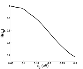
In reverse bias conditions, increasing the voltage amplitude limits the spin polarization of injected electrons due to a transport across a wider depletion region with enhanced electric field Albrecht_PRB03 ; Saikin_JPCM04 ; Weng_PRB04 and due to an enhanced spin relaxation of injected electrons prior to their thermalization Saikin_JPCM06 ; Mallory_PRB06 ; Song_CondMat09 . The detrimental effect of the former can be overcome by increasing the doping concentration next to the junction. However, the second effect is an intrinsic property that cannot be engineered for a given zinc-blende bulk semiconductor. Fig. 3 shows the fraction of the net injected spin that is left after the energy thermalization process as a function of the injected energy in a 1016 cm-3 n-type GaAs Song_CondMat09 . The spin information is largely kept when the energy of injected electrons is less than 0.1 eV. These results are also in accordance with recent measured data by Crooker et al. Crooker_PRB09 . The spin relaxation of these hot electrons is governed by the Dyakonov-Perel mechanism Dyakonov_JETP33 ; Optical_Orientation . Due to the moderately reverse biased GaAs/Fe junction, we have assumed that the injected electrons tunnel into the -valley of the conduction band. Thus, the energy thermalization is governed by emission of long wavelength LO-phonons Born_Book . This scenario is valid if the injected energy of hot electrons is less than 0.3 eV above the -point of conduction band in GaAs. At stronger reverse bias conditions, the injected electrons can reach the -valley and thus experience strong inter-valley scattering processes Yu_Cardona . In the case of a 1016 cm-3 n-type GaAs at room temperature, this injection energy limit corresponds to a 0.4 V reversed biased GaAs/Fe junction (the Fermi energy is about 0.1 eV below the conduction band).
We conclude that if the bias voltage across the SC/FM is moderate then one can neglect the spin relaxation processes during the ultra-fast thermalization of injected electrons to the bottom of the conduction band. This allows one to match the spin polarized tunneling current densities with the spin polarized current densities at the edges of the bulk semiconductor region (Eq. (15)).
III.3 Intrinsic Capacitance of the Schottky barriers
In every moment of time, the applied potential fulfills the Laplace equation, with boundary conditions given by the charge current densities at the interfaces, . In the time-dependent case the charge current density also includes a displacement current density connected with charging or discharging the barrier capacitance (changing the width of the depletion layer),
| (45) |
is the voltage drop across the junction and is the barrier capacitance per unit area whose magnitude is given by the ratio between the static dielectric constant and the width of the Schottky barrier (typically of the order of F/cm2). In the following simulations, we will include the contribution of this current as part of the boundary conditions. This current can have a strong effect on the dynamics in time scales of the order of .
Contrary to charge currents, the spin currents are negligibly affected by the displacement current. This is valid if the change in the width of the Schottky barrier, , is such that . To derive this condition, we recall that the spin current densities, , include terms of the order of . The displacement spin current density is proportional to . If we are interested in time scales of the order of or longer than the spin relaxation time () then one can readily derive the above condition. Neglecting the contribution of the displacement current is robust even at faster time scales since low voltage signals change the width of a heavily doped Schottky barrier by only a few nm (). Barriers that are not heavily doped are of no interest due to the resulting negligible spin accumulation.
IV Results and Discussion
In showing the results of the presented theory we focus on two aspects. First, by using a steady state analysis we show how the spin transport in a semiconductor channel is affected by the escape current density and by the non-linear J-V relation across the SC/FM junctions. When contrasted with conventional spin transport analyses the results are significantly different . Second, by using a dynamical analysis we study the non-collinear magnetization configuration effect on the spin accumulation and current signals. The static and dynamical transport analyses are performed on a lateral semiconductor channel covered by three ferromagnetic terminals. Fig. 4 shows two bias settings of the studied structure where in each case two terminals are biased and a third terminal is connected in series to an external capacitor (not to be confused with the intrinsic Schottky capacitance of each SC/FM junction). By perturbing the magnetization vector of the left or right terminals, the resulting transient charge current across the external capacitor allows us to study the spin dynamics in the semiconductor channel.
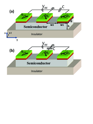
We perform simulations for applied voltage up to 0.3 V with all possible in-plane magnetization alignments at an interval of in each terminal. We recall that the boundary conditions across a SC/FM junction were derived using the assumption that the spin- axis is collinear with the majority spin direction in the FM (sections II.2 and III.1). However, in order to consider all (non-collinear) ferromagnetic terminals and the semiconductor channel as one system, one should use a single spin reference coordinate system. Specifically, we transform the general expressions in Eqs. (II.2) & (43) into this new ‘contact-independent’ coordinate system. The details of this transformation as well as the numerical procedure are explained in Appendix B. We use room temperature GaAs/Fe material system where the semiconductor parameters are: =1016 cm-3, =2700 cm2/Vs, =0.2 ns Kikkawa_PRL98 , =0.067. The Fermi wavevectors for majority and minority electrons in the iron terminals are, respectively, 1.1 and 0.42 where their mass is of free electrons Slonczewski_PRB89 . The doping and static dielectric constant in the Schottky barrier region are =21019 cm-3 and =1.1610-12 F/cm, respectively. The height of the barrier in equilibrium () is =0.7 eV from the ferromagnet’s Fermi energy. These barrier parameters yield a single localized energy level. In addition, the combined conductance (of both biased barriers) roughly matches the semiconductor spin-depth conductance (4104 cm-2). This allows us to study cases in which the spin polarization in the channel is relatively large ( is of the order of ). Spin injection experiments, on the other hand, are currently limited to much smaller polarization values due to the self-compensation issue of silicon donors in GaAs Adelmann_JVST05 . This limits the effective interface donor doping levels to 51018 cm-3 and the resulting conductance at room temperature to be less than cm-2 Hanbicki_APL03 . Breaking this impasse is a central challenge in the way to realize room temperature GaAs/Fe spintronics devices.
IV.1 Static Results
We use a steady state analysis to show the effects of the escape current density and of the non-linear J-V relation. First, we employ the setting of Fig. 4(a) in which the right terminal is outside the path of the steady state charge current. The magnetization directions of all three contacts are set parallel to the direction () so that is the only non-zero spin polarization component. The applied voltage is =0.3 V for which the resulting small voltage drop across each SC/FM junction justifies the use of our boundary conditions. Using these parameters, Fig. 5 shows a direct comparison of the spin polarization in the semiconductor channel between (a) the full model, (b) the model without the escape current mechanism and (c) the conventional model. Fig. 5(a) shows the result of the full model in which the boundary conditions are given by Eqs. (II.2), (42) & (43). Fig. 5(b) shows the case when only Eq. (II.2) is employed. Fig. 5(c) shows the results of the widely used conventional model in which not only the escape current mechanism is ignored but a linear form of Eq. (II.2) is used. This linear form is the set of Eqs. (32)-(35) with the replacement of the terms by . The conductance and finesses values in the conventional model are extracted around zero bias. Appendix A presents the calculation of the various reflection coefficient combinations whose integrations provide the conductance and mixing conductance values. In our simulations these values are =0.2, =2Re=6Im=2104 cm-2.
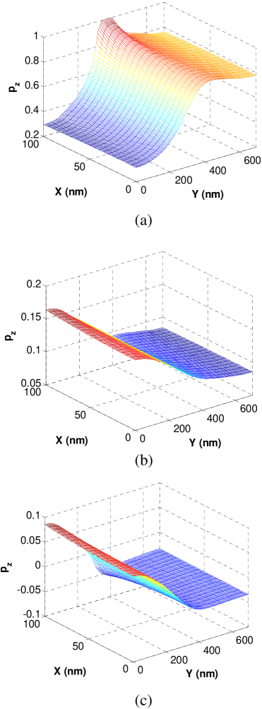
To understand the spin polarization in the semiconductor channel we consider two scenarios. In case (I), the transport across a reverse/forward biased junction is dominated by free/localized electrons. The net spin polarization produced by a ferromagnetic contact is therefore always aligned with the majority spin direction. Fig. 5(a) shows the results of this scenario. Case (II) assumes that free electrons dominate the transport regardless of the bias direction. In this case, the net spin polarization produced by a reverse/forward biased junction is aligned with the majority/minority spin direction of the contact. The results of such a scenario are depicted in Figs. 5(b) and (c). In non-collinear configurations, these rules can be generalized in the following way. In case (I)/(II), the net spin polarization vector in the semiconductor channel roughly points in the vector addition/substraction of the majority spin directions of the biased junctions.
We first explain the effect of the non-linear J-V relation via a comparison between the spin polarization in Figs. 5(b) and (c). The most distinct difference is the shift in values of . To understand this shift we recall of the Fermi level positions in the semiconductor channel and in the ferromagnetic terminal. In a non-degenerate semiconductor channel the values of the population distribution matrix are very small (0.05 in our simulated case). In very small reverse bias and in any forward bias the population distribution matrix of the FM, , is also very small for electrons that can tunnel to/from the semiconductor. The latter constraint is removed in higher reverse bias conditions where the ferromagnetic Fermi level reaches the conduction band edge of the semiconductor. This is the reason for the free electron asymmetrical current density at moderate bias conditions as seen from the inset of Fig. 2. The higher conductance of the reverse biased junction (when considering only free electrons) dictates the sign of the spin polarization in Fig. 5(b). On the other hand, in Fig. 5(c) the spin polarization is nearly symmetrical about the zero level at the biased part of the channel. To introduce asymmetry in the conventional model one has to artificially plug different conductance values for the forward and reverse biased junctions. However, due to the linear approximation around zero-bias, the formal derivation of the boundary conditions in the conventional model results in identical conductance values.
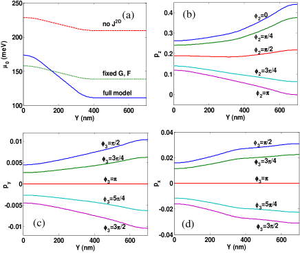
Fig. 5(a) highlights the unique behavior of the potential well in the interface doping area. We find the opposite of the conventional result which states that antiparallel configurations lead to a much larger spin polarization than parallel configurations Fert_PRB01 ; Dery_MCT_PRB07 . In collinear two-terminal systems the potential well flips the role of the parallel and antiparallel magnetization configurations (if we ignore the electrical field effect and assume that the channel length is smaller than the spin diffusion length.) The potential well significantly changes the shape of the spin accumulation where spins diffuse in opposite directions. This is seen by the opposite slopes of the spin polarization in the left part of the channel in Figs. 5(a) and (b). Notably, has a high plateau below the middle forward biased contact. Since the conductance of the forward biased junction increases when we incorporate the escape current mechanism, the relative portion of the voltage drop across the semiconductor channel increases and as a result the electric field in the channel increases. The field pushes spins carried by injected electrons to the direction and thus spins accumulate near the forward biased side. Studying this high spin-polarization regime is possible when working with rather than with its direction and with (Eq. (11)). Fig. 6(a) shows the -averaged electric potential along the semiconductor channel, . From the slope of the curves we can estimate the electrical field in the left part of the channel to be of the order of 2 kV/cm when incorporating the escape current mechanism and about four time smaller in the other cases. The resulting drift velocity () is still below the saturation velocity.
To explain the effect of the electric field on the spin currents we employ the full model with the setting of Fig. 4(b) and =0.1 V. Note that both charge and spin currents can flow in the semiconductor channel under the floating middle contact. Figs. 6(b)-(d) show the averaged spin components along the semiconductor channel (). As can be seen from Eq. (15), the signature of the electric field is evident at fields amplitudes which exceed Yu_Flatte_long_PRB02 (250 V/cm in non-degenerate n-type GaAs at room temperature). Fig. 6(b) shows the averaged component for five magnetization directions of the right biased contact whereas the other two contacts are set parallel in the direction (). The electric field opposes the diffusion of spins away from the forward biased junction and the spin polarization from the reverse biased junction spreads throughout the channel. This is the reason that even in the antiparallel configuration (), is not much into negative values beneath the forward biased (right) contact.
Figs. 6(c) and (d) show, respectively, the averaged and for . Here the non-collinearity of the floating middle contact (from to ) is the only drive for the and components. As before, the spin accumulation is pushed by the strong electric field toward the forward biased junction in the right part of the channel. The out-of-plane spin component is a useful probe of spin polarization beneath ferromagnetic contacts. For the chosen setting, we note that which is a direct result of the non-collinear middle contact is smaller than . The reason is that is a mixed term that is proportional to cross product of the spin polarization vector and the magnetization direction in the middle contact (). The spin-polarization in the channel is nearly collinear with the -axis because of the magnetization directions of the left and right biased contacts (==0). Taking, as an example, the case that the magnetization in the floating middle contact is along the -axis (=/2), then the mixed component can be larger than due to the relatively large in the channel. On the other hand, the component is generated by the very small voltage, , across the floating contact. This small bias results in a charge current density of magnitude which due to the external capacitor is contrasted by an equivalent charge current density of magnitude (nullifying the expression on the right hand side of Eq. (32) with ).
IV.2 Dynamic Results
We use a dynamical analysis to study how the non-collinearity affects the current signals. The setting of Fig. 4(a) is used where the magnetization direction of the middle terminal is fixed along (=0). The right terminal is outside the path of the steady state charge current, and its magnetization direction is perturbed according to for . The transient current across the external capacitor is then evaluated for various magnetization directions of the left terminal (). Similar dynamical setups have been suggested for collinear configuration by Cywinski et al. Cywinski_APL06 . Here, we allow for a more flexible operation regime (non-collinearity) and we offer a different physical interpretation of the dynamical results while emphasizing the robustness of the signals’ signature. Fig. 7 shows the transient currents across the external capacitor for four cases. The applied bias is 0.1 V, the external capacitance is fF, and the depth of the system in direction is 1 m. The magnetization direction of the right terminal completes a single clockwise rotation in =3 ns.
The transient currents in Fig. 7 are described by where is the potential level in the right terminal. This current is also the integrated current density at the right contact. This current density is given by,
| (46) | |||||
denotes the (small) self-adjusted voltage drop across the right terminal, and is the escape time at 0 voltage drop. The terms that involve are from linearizing Eq. (32) around V=0 and the term is due to the intrinsic capacitance of the Schottky barrier (Eq. (45); we use =10-6 F/cm2 in the simulations). The term that involves the step function, , is due to the escape of localized electrons (linearizing Eq. (42) around V=0). denotes the electron density in the potential well and . As discussed at the end of Sec. III.1, our modeling includes transport of localized electrons only at positive voltages. As a result, the effective barrier conductance is discontinuous at zero bias. This discontinuity is the reason for the ‘cusp’ points at times smaller than 3 ns in Fig. 7. Since we neglect the transport mechanisms that involve the potential well when 0, this discontinuity is a model dependent artifact. is the projected spin polarization vector on . The spin polarization vector is nearly constant and points in the vector addition of the majority spin directions of the biased ferromagnetic terminals (without considering the escape currents it would be the vector substraction). Thus,
| (49) |
For cases that , the discontinuity in at t= results in an additional ‘cusp’ point at this time (see Fig. 7 at t=3 ns). At times greater than 3 ns, is governed solely by the dynamics of towards its original value prior to the perturbation. At shorter times, is governed by the counteracting response of to the perturbing . This response aims at finding a new steady-state condition and its delay time is dictated by simple circuit analysis (see Fig. 1 in Ref. Cywinski_APL06 ). If the delay is much longer than the rotation time then can be viewed as static. In this case, by inspection of Eq. (46) we see that follows the shape of and its peak reaches an optimal value of (independent of the capacitance). The drawback of using a long delay is due to the slow dynamics at t. On the other hand, if the delay is very short then adiabatically follows . However, the resulting peak is now smaller (roughly) by the ratio of the delay and rotation times.
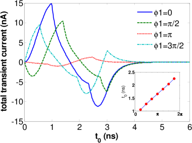
We use the above analysis to elucidate some of the general features of the current signals by concentrating on the case of Fig. 7. This curve shows two ‘cusp’ points around 1 ns and 2.35 ns. These are the times at which changes its sign. If the response time of the system was instantaneous (zero capacitance) then would have followed without a delay and these points would appear in 0.75 ns and 2.25 ns (where changes its sign). The reason for the longer delay in the first point (1 ns - 0.75 ns) than in the second point (2.35 ns - 2.25 ns) is due to the larger effective barrier conductance in forward bias. The initial current shape between 0 to 1 ns is due to the initial decrease of (Eq. (49) with =0). This change is counteracted by a 0.25 ns delayed increase of that tries to establish a new steady state. In the second branch, 1 ns2.35 ns, is positive in order to counteract the negative . The total transient current begin to decrease due to the turn-on of the escape current process. In the third branch, 2.35 ns3 ns, is positive again and the sudden current drop at 2.35 ns is due to the stop of the escape current (the component of the current is counteracted by a weaker and slower response of ). One can repeat this analysis for the other signals in Fig. 7. The difference in their shapes is governed by the phase term of . As a result, these signals have an apparent trend in shifting the time at which the current changes sign from positive to negative. This crossing time, denoted by , shows a linear dependence in as can be seen from the inset of Fig. 7.
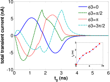
Fig. 8 shows the current signals for the opposite case in which the left magnetization is rotated and the right magnetization is set at various directions (with the same bias setting as before). We observe similar patterns. In this operational regime, the spin polarization vector changes in time beneath the right terminal whereas is constant. The response time is longer since the information needs to pass the delay of two (rather than one) Schottky barriers. For this setting, we denote as the time at which the signal switches sign from negative to positive. We observe a similar and nearly linear relation between and . However, the slope of the line is about twice as much then before. This double spacing is best explained with the vector addition rule we have provided in the static regime. The spin polarization vector in the semiconductor channel points roughly to the midway between and . Thus, the rotation speed of beneath the floating contact is about half that of . In terms of distinguishing different states, the second setting has a doubled time resolution compared with the previous case. If we employ =0.3 V, then the patterns of the signal in each setting are very close to the above cases, while the scale of the signal is about 3 to 5 times larger and the delay between and is shorter. Because of its physical origin, the current signal patterns are very robust and universal. Discussion about the coercivity and noise concerns can be found in Ref. Cywinski_APL06 .
IV.3 Configuration Analysis
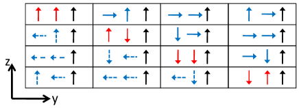
In this part we explore the maximal number of configurations that can possibly be stored in a system (as well as how to implement them). When two biased ferromagnetic contacts have a certain magnetization alignment, the spin polarization vector results in a unique setting in the semiconductor channel. The vector is more or less constant throughout the channel if the spin diffusion length is longer than the channel. Thus, this vector labels the particular magnetization configuration. One way to gain access to this vector information is to measure the total resistance of the two terminal system Brataas_PRL00 . This measurement can tell the relative angle but not the magnetization direction of each contact. In order to extract the information stored in these magnetization directions completely, we add a third ferromagnetic contact, floating or semi-floating, on top of the same semiconductor channel. We use the setting of Fig. 4(a) where the third magnetization direction provides a reference direction.
We have shown the physical connection between the measured signal and its magnetization configuration in the previous part, but we still need a systematical analysis to quantify the high density storage capacity in the designated circuit. This analysis is based on symmetry considerations. We will assume that in each contact there are two mutually perpendicular easy axes, determined by the semiconductor crystal orientation and by the thickness and shape of the ferromagnetic contact Kneedler_PRB97 . Fig. 9 shows all of the possible magnetization configurations. The right magnetization is unchanged due to the system rotational invariance to voltage or current measurement ( serves as a reference direction). In principle, there are 10 distinct voltage output values for these 16 configurations (the output is the voltage difference between the floating contact and the ground). It is less than 16, because the voltage of the floating contact is decided by and beneath it and thus the voltage has another invariance when the magnetization alignment is symmetric about . The four configurations on the ‘diagonal’ of the table in Fig. 9 have a unique output, whereas the ‘off-diagonal’ configurations are symmetric. The degeneracy of the voltage signal of all six ‘off-diagonal’ pairs can be lifted by fixing and while turning the direction by and repeating the measurement. Each configuration then has a unique combination of two results. In fact, performing two static measurements for different directions is equivalent to rotating in a given direction and measuring the transient current dynamically, as showed in the first setting in Sec. IV.2. In the dynamical method, we can completely distinguish all 16 states with a single measurement. The given rotation direction serves to break the symmetry about . The dynamic determination scheme is suitable for high frequency operation regime by properly selecting the external capacitor such that the signals are less affected by the noise Cywinski_APL06 ; Dery_Nature07 .
V Summary and Outlook
We have presented a detailed model that describes the spin transport in hybrid semiconductor/ferromagnet systems. The derivation of the transport equations and their boundary conditions are then used to model lateral hybrid systems with general non-collinear magnetization configurations. We have corrected the arguments that lead to the use of the quasi-neutrality approximation and explain their momentum and dielectric relaxation times dependence. The spin currents due to tunneling of free electrons across a semiconductor/ferromagnet junction were derived using a rigorous non-linear bias dependence of the tunneling current. The bias voltage limitations of spin injection and extraction were also discussed.
We have introduced an important contribution to the junction tunneling current that is governed by the escape of localized electrons. This process is a result of the usually employed inhomogeneous doping at the vicinity of the semiconductor/ferromagnet interface. The escape current is incorporated to the boundary conditions in forward bias. If the doping inhomogeneity is large then this process becomes the dominant current mechanism and as a result the spin accumulation patterns of parallel and anti-parallel configurations are flipped (compared to the case that only delocalized electrons are considered). We have provided simple rules for estimating the direction and magnitude of the spin-polarization vector in a semiconductor channel that is covered by spin selective and biased ferromagnetic contacts. Our results illustrate the importance of using impedance matched tunneling barriers with the semiconductor spin-depth conductance. This matching condition enables a large spin polarization even if the spin-selective barriers are not ideal. We have introduced a dynamical method that can clearly identify the non-collinear magnetization configuration from a three-terminal lateral structure. The amplitude and pattern of the current signals were explained using a spin dependent circuit analysis that incorporates the capacitive nature of the semiconductor/ferromagnet junction. The presented dynamical method can be used in spintronics devices for storage beyond the binary limit.
This work is supported by DOD/AF/AFOSR FA9550-09-1-0493 and by NSF ECCS-0824075.
Appendix A Barrier Structure Details
This appendix elaborates on the model that we use to calculate the localization energy () and the energy resolved reflection coefficients ( & ). These parameters depend on the voltage and are needed for calculating the spin dependent direct and mixing conductances (Eqs. (30) & (31)), as well as the escape times from the potential well (Eq. (37)).
Fig. 10(a) shows the energy profile that we use to calculate the localization energies and the spin-dependent reflection coefficients. is the voltage drop across the junction. The conduction band energy in the bulk semiconductor is the reference level (=0). The Schottky barrier height is =0.7 eV from the Fe Fermi energy which is =4.5 eV (=0.67 eV) for majority (minority) electrons from the bottom of the ferromagnetic conduction band Slonczewski_PRB89 . In the semiconductor, the doping in the bulk and barrier regions are =1016 cm-3 and =21019 cm-3, respectively. The effective masses are 0.067 in GaAs and in Fe. The Schottky barrier is located in the region where the conduction band is parabolic (obeying the Poisson equation). The doping inhomogeneity between the bulk and the interface regions generates a potential well next to the barrier Zachau_SSC86 -Shashkin_Semiconductors02 . We model this well by a flat potential region from to and then by a gradual linear increase to the bulk level from to . The width of the potential well in its flat region, , is governed by the voltage drop across the junction (). It shrinks/expands with increasing in reverse/forward bias conditions. This flat region vanishes at a reverse bias of -0.2 V where 8.5 nm. The depth of the potential well with respect to the conduction band of the bulk region is . The gradual region width is =4 nm. The geometrical details of this approximated profile do not substantially change the results of a rigorous self-consistent Schrodinger-Poisson equation set Dery_PRL07 ; Li_APL09 .
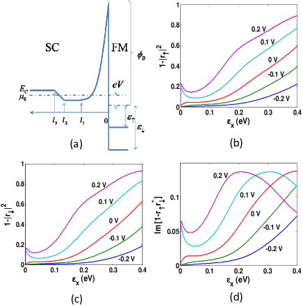
The spin dependence of the reflection coefficients is governed by the different Fermi velocities in the ferromagnetic region. We calculate these coefficients by assuming specular transport across the junction and applying a transfer-matrix method for the above energy profile (bold line in Fig. 10(a)). Figs. 10(b)-(d) show the spin dependent transmission coefficients and the imaginary part of the mixing term as a function of the longitudinal energy (kinetic energy along the GaAs/Fe interface normal). The real part of the mixing term satisfies 2Re, in agreement with the conclusion in Ref. Brataas_EPJB01 . The potential well leads to a relatively strong transmission of low energy free electrons (Ramsauer-Townsend resonance). This is shown by the peak at low regime in each of the curves. The summation over the kinetic energy in the parallel plane smears this peak in the I-V curve (inset of Fig. 2).
To calculate the localization energy we solve the Schrodinger equation for the semiconductor part of the energy profile (and replace the ferromagnetic part with an infinitely thick barrier whose height is ). This profile yields a single localized energy level in [-0.2 V, 0.2 V] and its value is essentially linear from -0.096 eV to -0.13 eV. We then calculate (Eq. (37)) and from .
Finally, we present an analytical model for the case of a simple rectangular barrier. This model is then used to extract the direct and mixing conductance values. The reflection coefficient of a rectangular barrier with width , and with barrier height from the ferromagnetic potential level () is given by Ciuti_PRL02 ,
| (50) | |||||
The wavevectors & are along the normal of the SC/FM interface. and are, respectively, the electron effective mass in the semiconductor and ferromagnet. The spin selectivity of the reflection is solely due to the spin dependent wavevectors in the ferromagnetic contact, .
Spin injection is possible when two conditions are met,
| I. | (51) | ||||
| II. | (52) |
where . In triangular or parabolic shapes we render the same conditions since the numerical values of effective are somewhat less but of the same order. The first condition guarantees a resistive rather than an ohmic contact Schmidt_PRB00 ; Rashba_PRB00 . The second condition guarantees that tunneling is the dominant transport mechanism across the barrier whereas the thermionic current is negligible. By increasing the electrons energy, condition II makes the Boltzmann tail of the population distribution decay faster than the increase in the transmission coefficient, . Thus, the main contribution to the current is from electrons whose energy is at the bottom of the conduction band. These conditions may also be used to simplify the calculation of the macroscopic conductances and finesse in rectangular barriers,
| (53) | |||||
| (54) | |||||
| (55) |
where one can see that 2Re, and is defined by,
In semiconductors with a small electron effective mass and in low bias voltages the finesse is approximately .
Appendix B Numerical Analysis
In this appendix, we discuss the techniques we use to solve the overall set of equations and we provide details about the numerical scheme. Essentially, we need to solve a system of four equations (Eq. (9) & Eq. (13)) with proper boundary and initial conditions. Boundary conditions for both the static and dynamic cases consist of the continuity of charge and spin current density. We render the non-approximated form of the free electrons boundary current densities (Eqs. (II.2)-(31)).
We discuss the static case first. When the system is in a steady state, the charge and spin current densities (Eqs. (14) & (15)) have no normal components at the boundaries that are not in contact with ferromagnetic terminals. In addition, the external capacitor forces a zero total charge current across the terminal that is attached to it. For boundaries with biased ferromagnetic terminals, the normal current density component is equal to the corresponding current density through the SC/FM junction. These current densities have been derived in Sec. II.2 and Sec. III.1 under the assumption that the -axis is collinear with the respective majority spin direction. However, in order to incorporate the three non-collinear ferromagnetic terminals and the semiconductor channel in a single system, we need to work with a contact-independent reference coordinate system. Specifically, we need to transform the expression in Eqs. (II.2) and (43) into the new coordinate system. We rewrite , and in these equations as , and to represent the contact-dependent coordinate. We reserve , and for coordinates in the contact-independent system. The current density expressions in these two sets of frames are related by
| (65) |
Note that the charge current density does not depend on the spin space coordinate. The components of the spin polarization also need to be expressed in terms of the components in the contact-independent system (by the reverse rotation transformation),
| (75) |
For time dependent simulations, we adopt a similar process except that we need to consider the displacement current due to capacitance embedded in the system. This includes the intrinsic capacitance of the Schottky barrier (Sec. III.3) and the external capacitor between ground and the semi-floating right terminal. The initial condition in the dynamical case is the steady state spin polarization and electrochemical potentials of its corresponding initial configuration.
We employ a finite difference method to obtain the spin polarization vector and the electrochemical potential in our multi-terminal system. The computational grid representing the two-dimensional semiconductor region has nodes with a 5 nm interval. A system of 4 differential equations is to be solved in this region. To obtain the desired accuracy, we use two major steps with iteration methods Ames ; Hoffman . Step I includes the evaluation of nonlinear coefficients using the under-relaxation method. These coefficients are updated periodically. Step II solves the linearized system of equations using an iterative technique, where we adopt the successive-over-relaxation method. For time dependent simulations, we generalize this procedure by using a Crank-Nicolson implicit method with a time interval of 0.02 ns. The space and time intervals are adjustable over several orders of magnitude, and we choose them in consideration of both the result details and the computation time.
References
- (1) I. Z̆utić, J. Fabian, and S. Das Sharma, Rev. Mod. Phys. 76, 323 (2004).
- (2) M. Johnson and R. H. Silsbee, Phys. Rev. B 35, 4959 (1987).
- (3) M. N. Baibich, J. M. Broto, A. Fert, F. Nguyen Van Dau, F. Petroff, P. Etienne, G. Creuzet, A. Friederich, and J. Chazelas, Phys. Rev. Lett. 61, 2472 (1988).
- (4) G. Binasch, P. Grünberg, F. Saurenbach, and W. Zinn, Phys. Rev. B 39, R4828 (1989).
- (5) J. S. Moodera, L. R. Kinder, T. M. Wong, and R. Meservey, Phys. Rev. Lett. 74, 3273 (1995).
- (6) G. A. Prinz, Science 282, 1660 (1998).
- (7) H. J. Zhu, M. Ramsteiner, H. Kostial, M. Wassermeier, H.-P. Schonherr, and K. H. Ploog, Phys. Rev. Lett. 87, 016601 (2001).
- (8) A. T. Hanbicki, B. T. Jonker, G. Itskos, G. Kioseoglou, and A. Petrou, Appl. Phys. Lett. 80, 1240 (2002).
- (9) B. T. Jonker, Proceedings of the IEEE 91, 727 (2003).
- (10) A. T. Hanbicki, O. M. J. van t Erve, R. Magno, G. Kioseoglou, C. H. Li, B. T. Jonker, G. Itskos, R. Mallory, M. Yasar, and A. Petrou, Appl. Phys. Lett. 82, 4092 (2003).
- (11) C. Adelmann, J. Q. Xie, C. J. Palmstrøm, J. Strand, X. Lou, J. Wang, and P. A. Crowell, J. Vac. Sci. Technol. B 23, 1747 (2005).
- (12) X. Jiang, R. Wang, R. M. Shelby, R. M. Macfarlane, S. R. Bank, J. S. Harris, and S. S. P. Parkin, Phys. Rev. Lett. 94, 056601 (2005).
- (13) I. Appelbaum, B. Q. Huang, and D. J. Monsma, Nature 447, 295 (2007).
- (14) B. T. Jonker, G. Kioseoglou, A. T. Hanbicki, C. H. Li, and P. E. Thompson, Nature Physics 3, 542 (2007).
- (15) B.-C. Min, K. Motohashi, C. Lodder, and R. Jansen, Nature Materials 5, 817 (2006).
- (16) L. E. Hueso, J. M. Pruneda, V. Ferrari, G. Burnell, J. P. Valdés-Herrera, B. D. Simons, P. B. Littlewood, E. Artacho, A. Fert, and N. D. Mathur, Nature 445, 410 (2007).
- (17) B. Q. Huang, D. J. Monsma, and I. Appelbaum, Phys. Rev. Lett. 99, 177209 (2007).
- (18) W. H. Butler, X.-G. Zhang, X. Wang, J. van Ek, and J. M. MacLaren, J. Appl. Phys. 81, 5518 (1997).
- (19) Ph. Mavropoulos, O. Wunnicke and P. H. Dederichs, Phys. Rev. B 66, 024416 (2002).
- (20) O. Wunnicke, Ph. Mavropoulos, R. Zeller, P. H. Dederichs and D. Grundler, Phys. Rev. B 65, 241306(R) (2002).
- (21) Y. J. Zhao, W. T. Geng, A. J. Freeman, and B. Delley, Phys. Rev. B 65, 113202 (2002).
- (22) M. Zwierzycki, K. Xia, P. J. Kelly, G. E. W. Bauer and I. Turek, Phys. Rev. B 67, 092401 (2003).
- (23) T. J. Zega, A. T. Hanbicki, S. C. Erwin, I. Z̆utić, G. Kioseoglou, C. H. Li, B. T. Jonker, and R. M. Stroud, Phys. Rev. Lett. 96, 196101 (2006).
- (24) A. N. Chantis, K. D. Belashchenko, D. L. Smith, E. Y. Tsymbal, M. van Schilfgaarde, and R. C. Albers, Phys. Rev. Lett. 99, 196603 (2007).
- (25) S. Honda, H. Itoh, J. Inoue, H. Kurebayashi, T. Trypiniotis, C. H. W. Barnes, A. Hirohata, and J. A. C. Bland, Phys. Rev. B 78, 245316 (2008).
- (26) G. Schmidt, D. Ferrand, L. W. Molenkamp, A. T. Filip, and B. J. van Wees Phys. Rev. B 62, R4790 (2000).
- (27) E. I. Rashba, Phys. Rev. B 62, R16267 (2000).
- (28) A. Fert and H. Jaffrès, Phys. Rev. B 64, 184420 (2001).
- (29) D. L. Smith and R. N. Silver, Phys. Rev. B 64, 045323 (2001).
- (30) Z. G. Yu and M. E. Flatté, Phys. Rev. B 66, 235302 (2002).
- (31) J. D. Albrecht and D. L. Smith, Phys. Rev. B 68, 035340 (2003).
- (32) H. Dery, Ł Cywiński, and L. J. Sham, Phys. Rev. B 73, 041306(R) (2006).
- (33) E. I. Rashba, Appl. Phys. Lett. 80, 2329 (2002).
- (34) Ł Cywiński, H. Dery, and L. J. Sham, Appl. Phys. Lett. 89, 042105 (2006).
- (35) H. Dery, P. Dalal, Ł Cywiński and L. J. Sham, Nature 447, 573 (2007).
- (36) W. Shockley, G. L. Pearson, and J. R. Haynes, Bell System Tech. J. 28, 344 (1949).
- (37) C. Herring, Bell System Tech. J. 28, 401 (1949).
- (38) J. Bardeen, Bell System Tech. J. 28, 428 (1949).
- (39) H. Brooks, Technical report No. 181, Cruft Laboratory, Harvard University (Cambridge, Massachusetts, 1953).
- (40) W. Van Roosbroeck, Bell System Tech. J. 29, 560 (1950); Phys. Rev. 123, 474 (1961).
- (41) M. Johnson, Science 260, 320 (1993).
- (42) F. J. Jedema, A. T. Filip, and B. J. van Wees, Nature 410, 345 (2001).
- (43) S. A. Crooker, M. Furis, X. Lou, C. Adelmann, D. L. Smith, C. J. Palmstrøm, and P. A. Crowell, Science 309, 2191 (2005).
- (44) X. Lou, C. Adelmann, M. Furis, S. A. Crooker, C. J. Palmstrøm, and P. A. Crowell, Phys. Rev. Lett. 96, 176603 (2006).
- (45) X. Lou, C. Adelmann, S. A. Crooker, E. S. Garlid, J. Zhang, K. S. Madhukar Reddy, S. D. Flexner, C. J. Palmstrøm, and P. A. Crowell, Nature Phys. 3, 197 (2007).
- (46) Y. Ji, A. Hoffman, J. E. Pearson, and S. D. Bader, Appl. Phys. Lett. 88, 052509 (2006).
- (47) D. Saha, M. Holub, and P. Bhattacharya, Appl. Phys. Lett. 91, 072513 (2007).
- (48) M. J. van ’t Erve, A. T. Hanbicki, M. Holub, C. H. Li, C. Awo-Affouda, P. E. Thompson, and B. T. Jonker, Appl. Phys. Lett. 91, 212109 (2007).
- (49) S. A. Crooker, E. S. Garlid, A. N. Chantis, D. L. Smith, K. S. M. Reddy, Q. O. Hu, T. Kondo, C. J. Palmstrøm, and P. A. Crowell, Phys. Rev. B 80, 041305(R) (2009).
- (50) Tunneling Phenomena in Solids, ed. E. Burstein and S. Lundqvist (Plenum Press, New York, 1969).
- (51) S. M. Sze, Physics of Semiconductor Devices (John Wiley, New York, 1981).
- (52) S. Zhang and P. M. Levy, Phys. Rev. B 65, 052409 (2002).
- (53) J. Zhang and P. M. Levy, Phys. Rev. B 71, 184417 (2005).
- (54) Y. H. Zhu, B. Hillebrands, and H. C. Schneider, Phys. Rev. B 78, 054429 (2008).
- (55) J. C. Slonczewski, Phys. Rev. B 39, 6995 (1989).
- (56) V. Ustinov and E. Kravtso, J. Phys. Condens. Matter 7, 3471 (1995).
- (57) H. E. Camblong, P. M. Levy and S. Zhang, Phys. Rev. B 51, 16052 (1995).
- (58) T. Valet and A. Fert, Phys. Rev. B 48, 7099 (1993).
- (59) A. Brataas, Y. V. Nazarov, and G. E. W. Bauer, Phys. Rev. Lett. 84, 2481 (2000).
- (60) D. H. Hernando, Y. V. Nazarov, A. Brataas, and G. E. W. Bauer, Phys. Rev. B 62, 5700 (2000).
- (61) A. Brataas, Y. V. Nazarov, and G. E. W. Bauer, Eur. Phys. J. B 22, 99 (2001).
- (62) Y. Xu, K. Xia, and Z. Ma, Nanotechnology 19, 235404 (2008).
- (63) S. Saikin, J. Phys. Condens. Matter 16, 5071 (2004).
- (64) Y. Song, J. Galkowski, and H. Dery (to be submitted for publication).
- (65) C. Ciuti, J. P. McGuire, and L. J. Sham, Phys. Rev. Lett. 89, 156601 (2002).
- (66) R. K. Kawakami, Y. Kato, M. Hanson, I. Malajovich, J. M. Stephens, E. Johnston-Halperin, G. Salis, A. C. Gossard, D. D. Awschalom, Science 294, 131 (2001).
- (67) R. J. Epstein, I. Malajovich, R. K. Kawakami, Y. Chye, M. Hanson, P. M. Petroff, A. C. Gossard, and D. D. Awschalom, Phys. Rev. B 65, 121202(R) (2002).
- (68) Y. Li, Y. Chye, Y. F. Chiang, K. Pi, W. H. Wang, J. M. Stephens, S. Mack, D. D. Awschalom, and R. K. Kawakami, Phys. Rev. Lett. 100, 237205 (2008).
- (69) V. V. Osipov and A. M. Bratkovsky, Phys. Rev. B 70, 205312 (2004).
- (70) H. Dery and L. J. Sham, Phys. Rev. Lett. 98, 046602 (2007).
- (71) P. Li and H. Dery, Appl. Phys. Lett. 94, 192108 (2009).
- (72) D. L. Smith and P. P. Ruden, Phys. Rev. B 78, 125202 (2008).
- (73) M. Zachau, F. Koch, K. Ploog, P. Roentgen, and H. Beneking, et al., Solid State Commun. 59, 591 (1986).
- (74) J. M. Geraldo, W. N. Podrigues, G. Medeiros-Ribeiro, and A. G. de Oliveira, J. Appl. Phys. 73, 820 (1993).
- (75) V. I. Shashkin, A. V. Murel, V. M. Daniltsev, and O. I. Khrykin, Semiconductors 36, 505 (2002).
- (76) B. Deveaud, J. Shah, T. C. Damen, and W. T. Tsang, Appl. Phys. Lett. 52, 1886 (1988).
- (77) T. Kuhn, in Theory of Transport Properties of Semiconductor NanoStructures, edited by E. Schöll (Chapman & Hall, London, 1998), pp. 173 214.
- (78) H. Dery, B. Tromborg and G. Eisenstein, Phys. Rev. B 67, 245308 (2003).
- (79) A. Malinowski, R. S. Britton, T. Grevatt, R. T. Harley, D. A. Ritchie, and M. Y. Simmons, Phys. Rev. B 62, 13034 (2000).
- (80) M. Q. Weng, M. W. Wu, and L. Jiang, Phys. Rev. B 69, 245320 (2004).
- (81) S. Saikin, M. Shen, and M. C. Cheng, J. Phys. Condens. Matter 18, 1535 (2006).
- (82) R. Mallory, M. Yasar, G. Itskos, A. Petrou, G. Kioseoglou, A. T. Hanbicki, C. H. Li, O. M. J. van t Erve, B. T. Jonker, M. Shen and S. Saikin, Phys. Rev. B 73, 115308 (2006).
- (83) Y. Song and H. Dery, cond-mat/0909.3124
- (84) M. I. Dyakonov and V. I. Perel, Sov. Phys. JETP 33, 1053 (1971); Sov. Phys. Solid State 13, 3023 (1972).
- (85) G. E. Pikus and A. N. Titkov, in Optical Orientation, edited by F. Meier and B. P. Zakharchenya, Vol. 8, 73-131 (Nort-Holland, New York, 1984).
- (86) M. Born and K. Huang, Dynamical Theory of Crystal Latticess (Oxford University Press, Oxsford, England, 1988).
- (87) P. Y. Yu and M. Cardona, Fundamentals of Semiconductors (Springer, Berlin, 1996).
- (88) J. M. Kikkawa and D. D. Awschalom, Phys. Rev. Lett. 80, 4313 (1998).
- (89) H. Dery, L. Cywinski, and L.J. Sham, Phys. Rev. B 73, 161307(R) (2006).
- (90) E. M. Kneedler, B. T. Jonker, P. M. Thibado, R. J. Wagner, B. V. Shanabrook, and L. J. Whitman, Phys. Rev. B 56, 8163 (1997).
- (91) W. F. Ames, Numerical Methods for Partial Differential Equations, 2nd ed. (Academic, New York, 1977).
- (92) J. D. Hoffman, Numerical Methods for Engineers and Scientists, 2nd ed. (CRC, New York, 2001).