Electron Transport in Disordered Graphene Nanoribbons
Abstract
We report an electron transport study of lithographically fabricated graphene nanoribbons of various widths and lengths at different temperatures. At the charge neutrality point, a length-independent transport gap forms whose size is inversely proportional to the width. In this gap, electron is localized, and charge transport exhibits a transition between simple thermally activated behavior at higher temperatures and a variable range hopping at lower temperatures. By varying the geometric capacitance through the addition of top gates, we find that charging effects constitute a significant portion of the activation energy.
pacs:
73.22.-b, 85.35.-pIn recent years graphene has been celebrated for its potential as a new electronic material Geim07 ; Geim08 . However, the absence of an energy band gap in graphene poses a challenge for conventional semiconductor device operations. Previous work Han07 ; Chen07 ; Li-Dai08 has shown that this hurdle can be overcome by patterning graphene into nanometer size ribbons or constrictions. The resulting transport gap formation can be most simply attributed to quasi 1-dimensional (1D) confinement of the carriers, which induces an energy gap in the single particle spectrum ManyGNRs . Detailed experimental studies of disordered GNRs Ponomarenko08 ; Stampfer09 ; Molitor09 ; Todd09 ; Liu08 ; Gallagher09 , , however, suggest that this observed transport gap may not be a band gap. In an effort to explain these experimental results, various theoretical explanations for the transport gap formation in disordered graphene nanostructures have been proposed, including models based on Coulomb blockade in a series of quantum dots Sols07 , Anderson localization due to edge disorder Gunlycke-White07APL ; Lherbier08 ; Evaldsson08 ; Querlioz08 ; Mucciolo09 ; Martin09 , and a percolation driven metal-insulator transition Adam08 . Further systematic experiment is necessary to distinguish between these different scenarios.
In this letter, we study the scaling of the transport gap in graphene nanoribbons (GNRs) with various widths and lengths at different temperatures. We find that four different energy scales can be extracted from transport measurement. From the scaling of these characteristic energies with GNR width and length, we find evidence of a transport mechanism in disordered GNRs based on hopping through localized states whose size is close to the width of the GNRs.
GNRs with different lengths () and a widths () were fabricated following the procedures described in Han07 . Most experiments in this report were performed on back-gated GNRs on a substrate of highly doped silicon with a 285 nm thick SiO2 gate dielectric. An example of such a device is shown in the inset to Fig. 1(a). We measured electron transport in a total of 41 GNRs with nm and m at different temperatures K. Additionally, we fabricated top-gated GNRs with 15 nm of hydrogen silsesquioxane (HSQ) and 10 nm of HfO2 as the gate dielectric material. The increased capacitive coupling allowed a comparative study of charging effects in back gated GNRs.
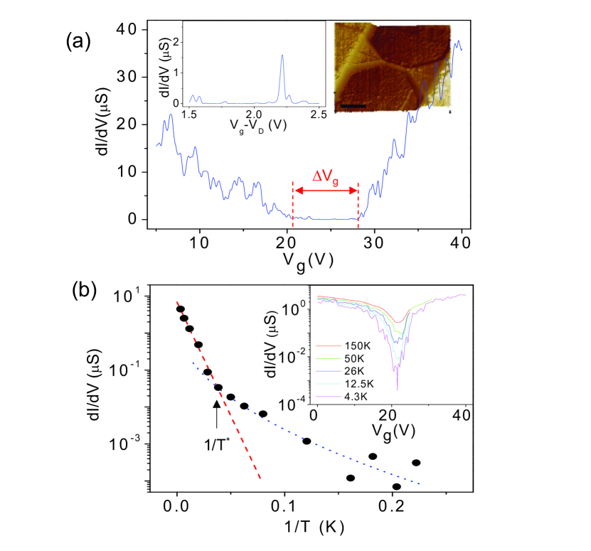
GNR conductance is strongly suppressed for a region of back gate voltages near the graphene charge neutrality point Han07 ; Chen07 ; Stampfer09 ; Molitor09 ; Todd09 ; Liu08 ; Gallagher09 , suggesting the formation of a transport gap. Fig. 1(a) shows low bias differential conductance as a function of for a typical GNR. The transport gap region in back gate voltage, , can be identified in this curve by extrapolating the smoothed to zero Stampfer09 ; Gallagher09 . We note that reproducible conductance peaks appear in the gap region Stampfer09 ; Molitor09 ; Gallagher09 (left inset Fig. 1(a)), which are indicative of resonant conduction paths through localized states inside the transport gap. In general, resonance peaks in the gap are less than 10 % of the values outside of the gap region.
The observed transport gap, corresponds to an energy in the single particle energy spectrum: , where m/sec is the Fermi velocity of graphene CastroNeto09 and is the capacitive coupling of the GNR to the back gate. This geometric capacitance is strongly dependent on ribbon dimensions and we calculate it using a finite element model, obtaining, for example, aF/m2 and meV for the particular device in Fig 1.
Away from the small resonant conductance peaks, the conductance is strongly suppressed in the transport gap, and the dominant charge transport can be described by thermally excited hopping between localized states footnote1 . We study the thermal activation of the off-resonant conduction in this regime by measuring , the minimum conductance for a given sweep of gate voltage , at different temperatures (inset to Fig. 1(b)). Fig. 1(b) shows an Arrhenius plot for . Evidently, thermally excited transport exhibits two distinct behaviors at low and high temperature regimes, respectively, separated by a characteristic temperature . At high temperatures (), the transport is simply activated: , where K is obtained from a linear fit of the Arrehenius plot (dashed line). At lower temperatures (), however, deviates from the simple activation behavior and decreases more slowly with decreasing temperature than the activated transport would imply. In this low temperature regime, the overall behavior is consistent with variable range hopping (VRH), where , with and a constant , determined by the characteristics of the localized states VRHref1 .
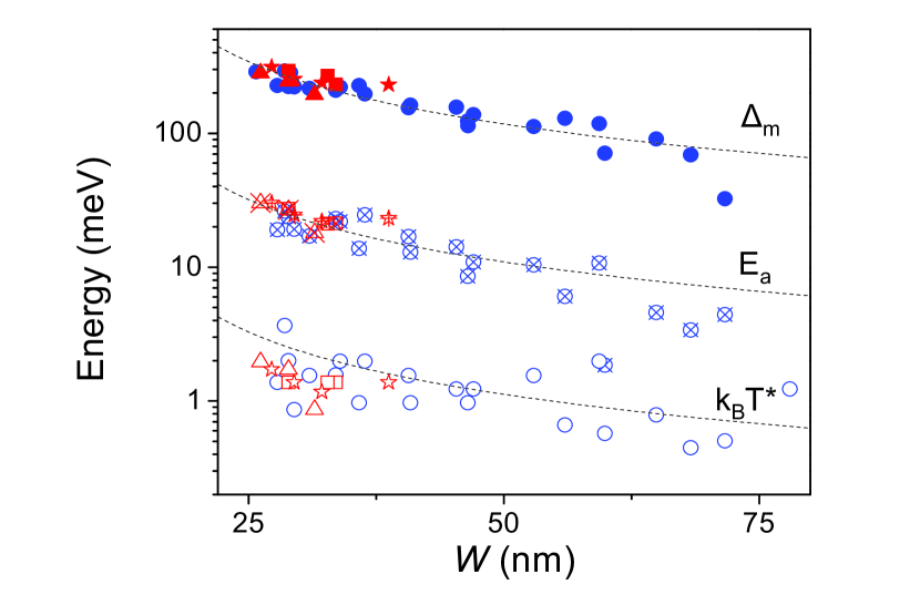
The aforementioned GNR transport gap and temperature dependent characteristics are typical of all GNRs with nm, so that , , and can be determined for each of these narrow GNRs. These three representative energy scales are plotted as a function of in Fig 2. In this graph, we note that (i) there is a clear separation between these energy scales, setting a general relation: for given ; (ii) , , and depend sensitively on but not ; and (iii) the energy scales are reasonably well described by inverse proportion to the lateral confinement of the GNR. The length independence can be noticed by comparing characteristic energies of the GNRs with similar but different (represented by different symbols in Fig. 2), and suggests that these three energy scales are 1D intensive properties of GNRs. To show this, we define the normalized width , where nm is the carbon-carbon bond length and is an offset introduced phenomenologically. Then, we find that all energy scales can be reasonably fit (dotted lines): ; ; with the proportionality parameters eV, eV, and meV, respectively, with nm held fixed for all three fits footnote2 .
Edge disorder in the GNRs tends to induce wavefunction localization, with a localization length that decreases rapidly with decreasing energy, resulting in a transport gap with strongly localized states at energies between the mobility edges Gunlycke-White07APL . The size of this mobility gap is larger than the clean band gap of an ideal ribbon; Querlioz et. al. calculate the scaling prefactor eV, averaged over many configurations of edge disorder Querlioz08 . The close match of our data to theoretical prediction supports the view that atomic defects at the graphene edges create localized states. We point out, however, that the observed energy scales lie within the range of disorder potential fluctuation created by the charged impurities in the SiO2 substrate Adam08 , making it difficult to exclude the contribution of a substrate disorder induced transport gap, as discussed in a recent experiment on transport in thermally annealed GNRs Gallagher09 .
On the other hand, ; i.e., the activation energy at higher temperatures is an order of magnitude smaller than . This observation excludes the scenario that extended states carry current via thermal activation across the transport gap. Instead, we interpret the simply activated behavior as a signature of 1D nearest neighbor hopping (NNH) through localized states within the transport gap Martin09 . In this picture, disorder at the edges tends to produce a rapid variation in the local density of states over the whole width of the ribbon, blocking the conductive paths and leading to a quasi-1D arrangement of localized states Evaldsson08 . Martin and Blanter predict Martin09 that the energy spacing between nearest neighbor states is determined by , where is the hopping matrix element between second nearest neighbor carbon atoms in graphene, so that eV Martin09 . Our measured value for this scaling prefactor, 3.39 eV, is somewhat larger than this prediction, which may be explained by the contribution of a charging energy to the hopping energy , discussed in more detail below.
The change of the transport behavior across the temperature allows a further comparison of our data to theory. In a very recent theoretical work, the NNH and VRH crossover is calculated to occur at , where was estimated numerically FoglerPreprint . In our experiment, we obtain , reasonably consistent with this theoretical prediction, lending further support to a model of charge transport via thermally activated hopping between localized states.
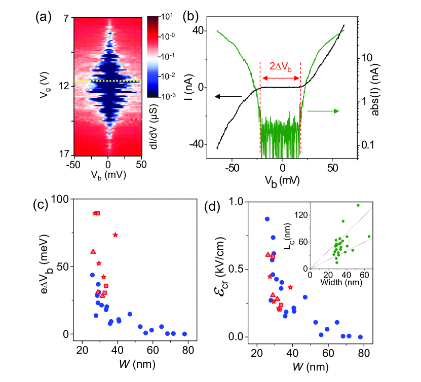
An alternative approach to probing the GNR transport gap is measurement of the non-linear transport characteristics Han07 . Fig. 3(a) shows differential conductance, as a function of and source-drain bias voltage . Transport through the GNR at finite shows a strong non-linear characteristic when is in the transport gap regime, which is most extreme when is near the charge neutrality point of the GNR (Fig. 3(b), black curve). The non-linear gap can be defined where a steep increase of current appears in logarithmic scale (Fig. 3(b), green curve).
In our previous study Han07 , the energy corresponding to was interpreted to be the band gap of the GNR. However, this naive interpretation should be carefully reconsidered for edge disordered GNRs, where the charge transport is dominated by hopping through localized states. Indeed, from the plot of vs (Fig 3(c)), we notice that depends strongly on , and is not well determined by alone, unlike the previous three characteristic energy scales (, , and ). Since the charge transport in the disordered GNRs is diffusive, it is likely that electric field is driving transport in the transport gap. Indeed, if we convert into the corresponding critical electric field , we restore a reasonable scaling behavior, where depends only on and not on (Fig. 3(d)).
In disordered systems in which transport is dominated by hopping through localized states, applied electric field plays a similar role to temperature. Thus we can treat the electric field as an effective temperature: , where is the averaging hoping length between localized states Shklovskii1973hci . Noting that the transition from NNH dominated transport to VRH transport occurs at , we can estimate . For most GNRs in this experiment we find that (Fig. 3(d) inset). The fact that supports our claim that hopping transport through the ribbons is effectively 1D.
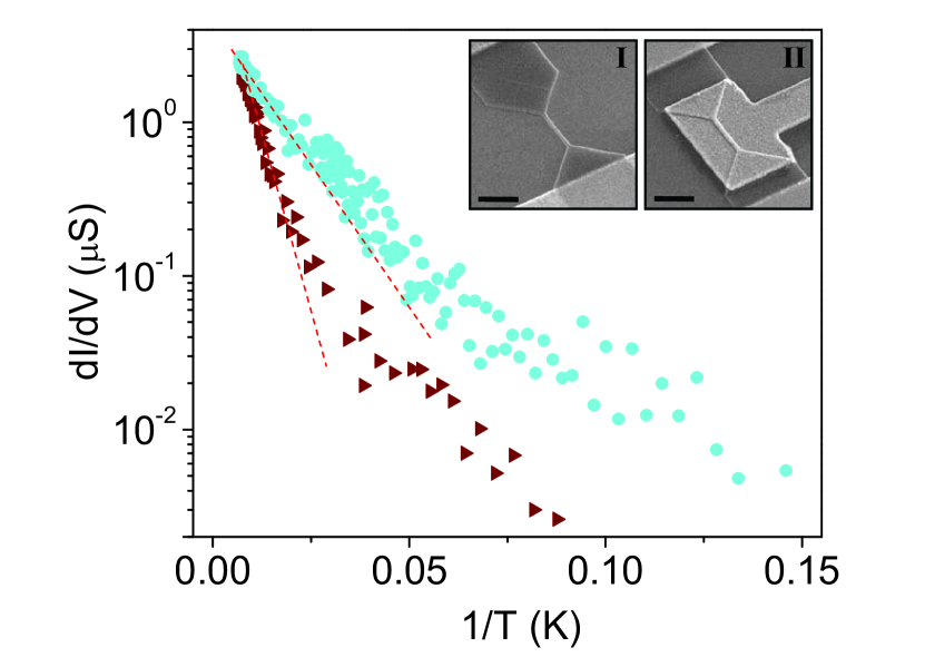
Finally, we discuss the effect of Coulomb charging in GNRs. Several previous works have discussed the role of Coulomb blockade and charging effects on the transport gap in GNRs and graphene constrictions Sols07 ; Stampfer09 ; Gallagher09 . In principle, in a GNR with hopping between localized states, we expect Coulomb interactions to open a soft Coulomb gap near the Fermi surface, which can be incorporated into the total hopping energy in addition to the single particle energy level spacing , so that , where is the Coulomb charging energy. Martin09 ; Fogler2004vrh ; Efros-Shklovskii85Book-p409 . In order to quantify the contribution of charging energy to the hopping energy , we perform a comparative transport measurement on GNRs with different gate coupling. Fig. 4 shows the temperature dependent minimum conductance for a back gate only GNR (device I) and a GNR with both top and back gates (device II) with the similar and . While device I has usual capacitive coupling to the back gate, (i.e., ), for device II is much closer to the top gate, leading to a larger capacitance: . From the thermally activated Arrhenius behaviors in the high temperature regime (dashed lines), we obtain the activation energies of the two devices, meV and meV averaged over two devices of type I and four of type II. Considering the smaller charging energy contribution for a top gated device, smaller values of the activation energy are indeed expected, if Coulomb effects are appreciable in the GNR.
Employing the ratio , we now can estimate the charging energy contribution quantitatively. Assuming that the single particle energy level spacing is similar for both GNRs due to their similar dimensions, we obtain , where the charging energy ratio of device I and II are given by . The resulting estimate for the charging energy contribution, , indicates that the Coulomb charging effect provides a substantial portion of the activation energy.
In conclusion, we investigate length and width dependent resistance scaling in GNRs. Temperature dependent and electric field dependent transport characteristics indicate that charge transport in the transport gap of the disordered GNR is dominated by localized states, where the Coulomb charging effects play an important role.
The authors thank M. Fogler, I. Martin, K. Ensslin, D. Goldhaber-Gordon, A. Young, P. Cadden-Zimansky, I. Aleiner, and B. Altshuler for helpful discussion. This work is supported by the ONR MURI, FENA, NRI, DARPA CERA. Sample preparation was supported by the DOE (DE-FG02-05ER46215). JCB was supported by CNPq, Brazil.
References
- (1) A. K. Geim and K. S. Novoselov, Nat Mater 6, 183 (2007).
- (2) A. K. Geim and P. Kim, Scientific American 298, 68 (2008).
- (3) M. Y. Han et al., Phys. Rev. Lett. 98, 206805 (2007).
- (4) Z. Chen et al.Physica E 40, 228 (2007).
- (5) X. Li et al., Science 319, 1229 (2008).
- (6) K. Nakada et al., Phys. Rev. B 54, 17954 (1996); K. Wakabayashi et al., Phys. Rev. B 59, 8271 (1999); M. Ezawa, Phys. Rev. B 73, 045432 (2006); Y. W. Son, M. L. Cohen, and S. G. Louie, Phys. Rev. Lett. 97 216803 (2006); L. Brey and H. A. Fertig, Phys. Rev. B 73, 235411 (2006); V. Barone, O. Hod, and G. E. Scuseria, Nano Letters 6, 2748 (2006).
- (7) L. A. Ponomarenko et al., Science 320, 356 (2008).
- (8) C. Stampfer et al., Phys. Rev. Lett. 102, 056403 (2009).
- (9) F. Molitor et al., Phys. Rev. B 79, 075426 (2009).
- (10) K. Todd et al., Nano Letters 9, 416 (2009).
- (11) X. Liu et al., arXiv:0812.4038.
- (12) P. Gallagher, K. Todd and D. Goldhaber-Gordon, arXiv:0909.3886.
- (13) F. Sols, F. Guinea, and A. H. CastroNeto, Phys. Rev. Lett. 99, 166803 (2007).
- (14) D. Gunlycke, D. A. Areshkin, and C. T. White, Appl. Phys. Lett 90, 142104 (2007).
- (15) A. Lherbier, et al., Phys. Rev. Lett. 100, 036803 (2008).
- (16) M. Evaldsson et al., Phys. Rev. B 78, 161407(R) (2008).
- (17) D. Querlioz et al., Appl. Phys. Lett. 92, 042108 (2008).
- (18) E. R. Mucciolo, A. H. Castro Neto, and C. H. Lewenkopf, Phys. Rev. B, 79, 075407 (2009).
- (19) I. Martin and Y. M. Blanter, Phys. Rev. B 79, 235132 (2009).
- (20) S. Adam et al., Phys. Rev. Lett. 101, 046404 (2008)
- (21) Since the typical size of the transport gap in the GNRs in this work is much larger than the thermal energy, we ignore thermally excited transport via delocalized states outside of the gap.
- (22) N. F. Mott, Phil. Mag.,19, 835 (1969).
- (23) A. H. CastroNeto et. al, Rev. Mod. Phys. 81, 109 (2009).
- (24) This offset can either be ascribed to the critical length scale of the edge localized states [3, 16], to the critical percolation length scale [20], or to simply experimental inaccuracy of the width determination due to over-etching underneath the etch mask [3].
- (25) A. S. Rodin and M. M. Fogler, arXiv:0909.0320.
- (26) M. M. Fogler, S. Teber, and B. I. Shklovskii, Phys. Rev. B 69, 035413 (2004).
- (27) B. I. Shklovskii, Sov. Phys. Semicond 6, 1964 (1973).
- (28) A. L. Efros and B. I. Shklovskii, in Electron-Electron Interactions in Disordered Systems, edited by A. L. Efros and M. Pollak (North-Holland, Amsterdam, 1985), p. 409.