Controllable Andreev retroreflection and specular Andreev reflection in a four-terminal graphene-superconductor hybrid system
Abstract
We report the investigation of electron transport through a four-terminal graphene-superconductor hybrid system. Due to the quantum interference of the reflected holes from two graphene-superconductor interfaces with phase difference , it is found that the specular Andreev reflection vanishes at while the Andreev retroreflection disappears at . This means that the retroreflection and specular reflection can be easily controlled and separated in this device. In addition, due to the diffraction effect in the narrow graphene nanoribbon, the reflected hole can exit from both graphene terminals. As the width of nanoribbon increases, the diffraction effect gradually disappears and the reflected hole eventually exits from a particular graphene terminal depending on the type of Andreev reflection.
pacs:
74.45.+c, 73.23.-b, 74.78.NaGraphene, a single layer honeycomb lattice consisting of carbon atoms, has attracted considerable attentions in condensed matter community recently.ref1 ; ref2 ; ref3 ; ref4 The unique band structure of graphene with a linear dispersion relation near the Dirac-points leads to many peculiar properties, such as the low-energy Dirac-like quasi-particle dispersion relation and the relativistic-like behaviors.ref3 ; ref4 Very recently, people begun to investigate graphene-superconductor hybrid systems.ref5 ; ref6 ; ref7 ; ref8 ; aref1 ; ref9 A unique and interesting phenomenon, the specular Andreev reflection (different from the usual Andreev reflection), was predicted to occur at the interface of the graphene and superconductor.ref5 It was discovered fifty years ago,ref10 that near the interface of a conductor and superconductor an incident electron from the metallic side is retro-reflected as a hole and a Cooper pair is created in the superconductor, a process known as the Andreev reflection. When the bias is smaller than the superconductor gap, the conductance of the metal-superconductor hybrid device is mainly determined by the Andreev reflection. For the graphene-superconductor system, in addition to the Andreev retroreflection, an unusual Andreev reflection, the specular Andreev reflection may occur, in which the direction of reflected hole is along the specular direction.ref5 From the band structure point of view, if electron-hole conversion is intraband: both incident electron and reflected hole are from the same band (conduction or valence band), this corresponds to the usual Andreev retroreflection. The specular Andreev reflection occurs if the electron-hole conversion is interband: the incident electron and reflected hole are, respectively, in the conduction and valence bands. Note that in two-terminal superconductor-graphene device, both specular reflection and retroreflection occur. It is highly desirable to control and separate these Andreev reflections experimentally. It is the purpose of this letter to achieve this goal.
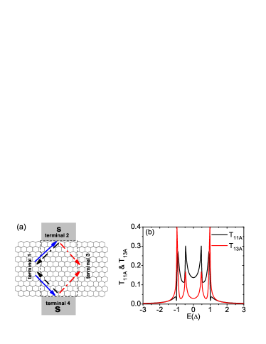
In this letter, we study a four-terminal graphene-superconductor device which consists of two superconductor terminals with the phase difference and two graphene terminals (see Fig.1a). By using the non-equilibrium Green function method, the current as well as the Andreev reflection coefficients are calculated. Our result shows that due to the quantum interference of reflected holes from two superconductor terminals 2 and 4 different Andreev reflection processes can be selected by tuning the phase difference . When only the Andreev retroreflection occurs and the specular Andreev reflection is prohibited while for only the specular Andreev reflection occurs and retroreflection vanishes. Therefore it is very easy to control the specular Andreev reflection and Andreev retroreflection by simply tuning the superconductor phase difference . In addition, the direction of the reflected hole, which is along either the graphene terminal-1 or terminal-3 depending on the type of Andreev reflection, can only be exhibited for large samples. When the sample size is comparable to the wavelength of reflected hole, however, the diffraction effect dominates so that the reflected hole can exit from both graphene terminals.
The four-terminals device we considered consists of a zigzag edged graphene nanoribbon sandwiched by two superconductor terminals, as shown in the Fig.1a.anote2 In the tight-binding representation, the Hamiltonian of the clean graphene nanoribbon is given byref12 , where () is the creation (annihilation) operator at the site . The on-site energy is the reference energy for Dirac-point, which can be controlled experimentally by the gate voltage. Two superconductor terminals are represented by BCS Hamiltonian, , where is the index of the superconductor terminal and with the superconductor gap and phase . The coupling between superconductor terminal and graphene is described by . Here is the horizonal position of the carbon atom and .ref13 So the total Hamiltonian is .
Using the Heisenberg equation of motion,ref14 the current flowing from the graphene terminal 1 to the scattering region is found to be
| (1) | |||||
where and are the Fermi distribution with the bias . Here we set the bias of two superconductor terminals be zero (). In Eq.(1), and are the normal transmission coefficients from the terminal 1 to the terminal , , and , respectively. and are the Andreev reflection coefficients for the incident electron coming from the terminal 1 with the hole Andreev reflected to the terminal 1 () or terminal 3 (). Here the subscripts , , , and represent the 11, 12, 21, and 22 matrix elements in Nambu subspace. The linewidth function is defined as and are the retarded (advanced) Green functions of central region in Nambu representation. with the Hamiltonian of the central region labeled by a rectangular area in Fig.1(a). is the retarded self-energy due to the coupling to the terminal . , where is the surface Green function of terminal . For the graphene terminal 1 and 3, we have to numerically calculate their surface Green function,ref15 while for superconductor terminal 2 and 4, the surface Green function ,ref13 where is the normal density of states, is the 0-th order Bessel function with the Fermi wave vector , and for and for . In numerical calculations, we set the hopping energy and the length of C-C bond as in a real graphene sample. The superconductor gap is set to be and the Fermi wave-vector .
We first study a three-terminal device by decoupling one of the superconductor terminal (2 or 4). Fig.1b shows the Andreev reflection coefficients and as a function of incident electron energies . It can be seen that and are quite large when the energy is within the gap () and exhibit peaks at the Dirac points and the gap edge .anote1 Similar to the usual normal-superconductor junction and decay quickly when is outside of the gap.ref16 . Note that when , the incident electron and reflected hole are in the same band (see Fig.3f) leading to the usual Andreev retroreflection. On the other hand, for , the incident electron and reflected hole are, respectively, in the conduction and valence bands (see Fig.3f) giving rise to the specular Andreev reflection. The above results show that both retroreflection and specular reflection occur with large amplitudes in the three-terminal device (with only one superconductor terminal).
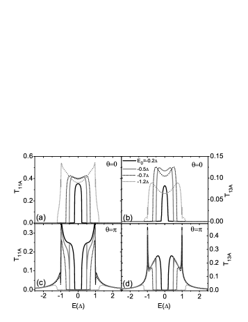
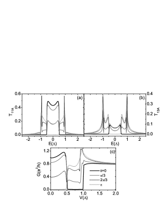
Next, we focus on the four-terminal device. Fig.2 shows and versus the energy for two different superconductor phase differences and . When , and are zero for but quite large for (see Fig.2a and 2b). This means that at only the retroreflection occurs and the specular reflection is prohibited. On the other hand, when , the situation reverses: and are zero for and quite large when (see Fig.2c and 2d). Hence when , the retroreflection is prohibited and only specular reflection occurs. Experimentally, the phase difference can be tuned by varying the super-current between two superconductor terminals. So the present four-terminal device gives us a handle to experimentally control and select the Andreev retroreflection and specular Andreev reflection.
Now we explain why the retroreflection disappears at the phase difference while the specular reflection vanishes at . In the four-terminal device with two graphene-superconductor interfaces, two Andreev reflections from each interface contribute coherently to the resultant Andreev reflection coefficient. Depending on the phase carried by each Andreev reflection, the interference can either be constructive or destructive. For the retroreflection, each reflected hole carries a phase factor,ref16 of the corresponding superconductor terminal, leading to a total Andreev reflection coefficient proportional to , whose value reaches the maximum at and minimum at . So the Andreev retroreflection disappear at due to the destructive interference. However, for the specular Andreev reflection, in addition to the phase difference , an extra phase is acquired due to the reflection between two interfaces when the incident electron and reflected hole involves different energy bands. The origin of this extra phase is similar to the junction of the superconductor-graphene-superconductor device,ref6 where a super-current of form was found. Due to this extra phase the total Andreev reflection coefficient is proportion to , whose value is zero at resulting a vanishing specular Andreev reflection at .
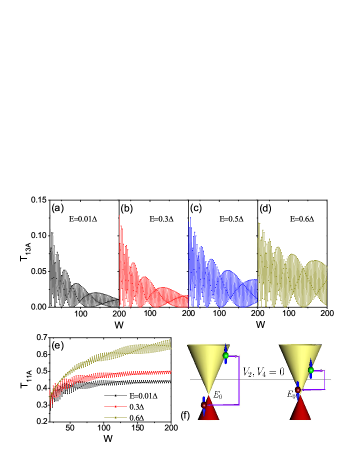
Since the reflected hole from the Andreev retroreflection (the specular Andreev reflection) is along the retro-reflected (the specular reflected) direction as shown in Fig.1a, Andreev reflection coefficient () should be zero at (). This does not agree with what we have obtained in Fig.2. We attribute this phenomenon to the diffraction effect of the reflected hole in the small device. To verify this statement, we have studied the size dependence of the Andreev reflection coefficient. Fig.3a-3e show and versus the width for , in which only the retroreflection occurs. With the increase of the width , oscillates and decays to zero while increases and saturates at large . This clearly indicates that the reflected hole exits only from the terminal-1 at large width . In addition, from the standing wave in the semi-infinite graphene ribbon, the wavelength of the reflected hole has been calculated. We found that when the graphene-ribbon width is in several tens this wavelength is on the same order of the device size. So for this width (several tens), the diffraction effect is significant. As a result, the reflected hole can exit from both terminal 1 and 3 leading to non-zero values of both and .
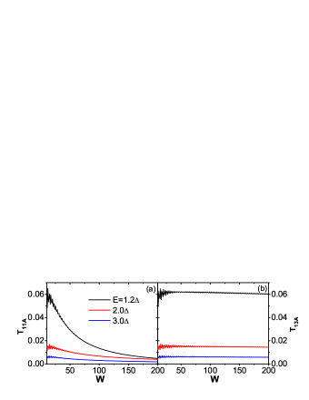
We now examine the size dependence of the specular Andreev reflection when . We expect that when the width of the graphene ribbon increases the reflected hole should go to the terminal 3 due to the fact that the diffraction effect disappears at large . Indeed, our numerical result confirms this. From Fig.4 we see that decays to zero and saturates at large .
From the above discussion, we see that when the wavelength of the reflected hole is comparable to the width of graphene nanoribbon, its direction can not be used to distinguish the Andreev retroreflection and specular Andreev reflection. Nevertheless, these two kinds of Andreev reflection can manifest their difference in the four-terminal device by tuning the superconductor phase as demonstrated above. This also shows that the electron-hole conversion mechanism, i.e., interband or intraband conversion, is the fundamental origin for these two kinds of Andreev reflections.
Up to now, we only considered the clean graphene ribbon at or . In the presence of the weak impurity disorder,ref20 all the results still remain, except that the boundary of two kinds of Andreev reflection slightly smeared. In addition, for other , both types of Andreev reflection may occur (see Fig.5a and 5b) due to the incomplete destructive interference. With the variation of from to , the specular reflection ( and at ) gradually increases from zero to the maximum value while the retroreflection ( and at ) gradually decreases from the maximum value to zero.
Finally, we investigate the differential conductance at zero temperature and discuss the experimental feasibility. By setting the bias and , the direct tunneling from the terminal 1 to the terminal 3 does not contribute to the current. The differential conductance is given by . At small bias , the normal tunneling processes from the terminal 1 to two superconductor terminal 2, 4 ( and ) are forbidden, so the conductance is directly related to the Andreev reflection coefficient . Fig.5c shows the conductance versus the bias at different . For , the specular Andreev reflection vanishes, so is zero at . On the other hand, for , the Andreev retroreflection disappears leading to at . Upon varying from to , the conductance at drops to zero while at gradually increases from . For the bias , is always large and weakly depends on the phase difference because of the contribution of the normal tunneling process. Note that experimentally the graphene nanoribbonsref17 have been realized with the superconductor leads attached to graphene nanoribbons.ref9 So the proposed device is within the reach of the present technology and is feasible experimentally.
In conclusion, the interplay of two kinds of Andreev reflections in a four-terminal graphene-superconductor hybrid device was investigated. It was found that the Andreev retroreflection and specular Andreev reflection can be tuned in this system due to quantum interference. When the superconductor phase difference , the specular Andreev reflection is prohibited and only the Andreev retroreflection occurs. However, for , the Andreev retroreflection is suppressed and only the specular Andreev reflection occurs. In addition, in the narrow graphene nanoribbon with its size comparable to the wavelength of the reflected hole, the diffraction effect occurs. Then the reflected hole can exit from both graphene terminals. On the other hand, for large samples, the diffraction effect disappears and the reflected hole can only traverse to a particular terminal depending on the kind of Andreev reflections.
Acknowledgments: The work is supported by NSFC under Grant Nos. 10525418, 10734110, and 10821403 and by 973 Program Project No. 2009CB929103 (Q.F.S.); a RGC grant from the Government of HKSAR grant number HKU 704308P (J.W.).
References
- (1) Electronic address: sunqf@aphy.iphy.ac.cn
- (2) K. S. Novoselov et al., Science 306, 666 (2004); K. S. Novoselov et al., Nature (London) 438, 197 (2005).
- (3) Y. Zhang et al., Nature (London) 438, 201 (2005).
- (4) C. W. J. Beenakker, Rev. Mod. Phys. 80, 1337 (2008).
- (5) A. H. Castro Neto, et al., Rev. Mod. Phys. 81, 109 (2009).
- (6) C. W. J. Beenakker, Phys. Rev. Lett. 97, 067007 (2006).
- (7) J. Linder, et al., Phys. Rev. Lett. 100, 187004 (2008).
- (8) Q. Y. Zhang, et al., Phys. Rev. Lett. 101, 047005 (2008); Q. Liang, et al., Phys. Rev. Lett. 101, 187002 (2008).
- (9) S. Bhattacharjee and K. Sengupta, Phys. Rev. Lett. 97, 217001 (2006); J. Cayssol, ibid. 100, 147001 (2008).
- (10) D. Rainis, et al., Phys. Rev. B 79, 115131 (2009).
- (11) H. B. Heersche, et al., Nature (London) 446, 56 (2007); F. Miao, et al., Science 317, 1530 (2007).
- (12) A. F. Andreev, Sov. Phys. JETP. 19, 1228 (1964).
- (13) For the armchair edged graphene ribbon and for the graphene ribbon with hydrogen passivation (see Y.-W. Son et al., Phys. Rev. Lett. 97, 216803 (2006)), an energy gap emerges around the Dirac point . So here we consider the usual zigzag edged graphene ribbon.
- (14) W. Long et al., Phys. Rev. Lett. 101, 166806 (2008).
- (15) Q.-F. Sun and X.C. Xie, J. Phys.: Condens. Matter 21, 344204 (2009).
- (16) Y. Meir and N.S. Wingreen, Phys. Rev. Lett. 68, 2512 (1992); N. S. Wingreen et al., Phys. Rev. B 48, 8487 (1993).
- (17) D. H. Lee and J.D. Joannopoulos, Phys. Rev. B 23, 4997 (1981); M. P. Lopez Sancho, et al., J. Phys. F: Met. Phys. 14, 1205 (1984); 15, 851 (1985).
- (18) Here at and at originate from the diffraction effect in the small-size device.
- (19) G. E. Blonder, et al., Phys. Rev. B 25, 4515 (1982); G. Deutscher, Rev. Mod. Phys. 77, 109 (2005).
- (20) J. Martin, et al., Nature Phys., 4, 144 (2008).
- (21) X. Li, et al., Science 319, 1229 (2008).