Metal-insulator transition through a semi-Dirac point
in oxide nanostructures: VO2 (001) layers confined within TiO2
Abstract
Multilayer (TiO2)m/(VO2)n nanostructures ( - interfaces with no polar discontinuity) show a metal-insulator transition with respect to the VO2 layer thickness in first principles calculations. For 5 layers, the system becomes metallic, while being insulating for = 1 and 2. The metal-insulator transition occurs through a semi-Dirac point phase for = 3 and 4, in which the Fermi surface is point-like and the electrons behave as massless along the zone diagonal in k-space and as massive fermions along the perpendicular direction. We provide an analysis of the evolution of the electronic structure through this unprecedented insulator-to-metal transition, and identify it as resulting from quantum confinement producing a non-intuitive orbital ordering on the V ions, rather than being a specific oxide interface effect. Spin-orbit coupling does not destroy the semi-Dirac point for the calculated ground state, where the spins are aligned along the rutile -axis, but it does open a substantial gap if the spins lie in the basal plane.
I Background
VO2 in its bulk form displays a metal-insulator transition (MIT) which occurs near RT (at approximately 340 K).Morin (1959) This change in the electronic structure is accompanied by a structural distortion that involves the dimerization (to a low-temperature monoclinic insulating phase) of the V chains that form in the rutile structure, leading to a V-V singlet state accompanied by the expected reduction of the magnetic susceptibility.Goodenough (1971) The direct V-V exchange along the chains forms spin-singlets at low temperature, that break up above 340 K leading to a structural distortion, with dimers no longer occurring and V-V distances becoming uniform along the rutile c-axis. This MIT has been widely studied, with effort given to tuning the temperature of the transition,Muraoka and Hiroi (2002) because its proximity to RT makes it usable for various applications.Strelcov et al. (2009); Wei et al. (2009)
Recently oxide interfaces (IF) have shown interesting (and not yet well understood) MITs. One of these happens with a few layers of LaAlO3 (LAO) on top of a SrTiO3 (STO) substrate. Here, the effects of having a polar IF come into play, producing an electric field within the LAO layer that raises the energies (bands) of successive layers. Calculations show that the onset of the overlap of valence band O states at the surface with Ti conduction states on the substrate produces an insulator-to-metal transition in the heterostructure around 4 layers of LAO grown on an STO substrate,Pentcheva and Pickett (2006); Siemons et al. (2007); Park et al. (2006); Pentcheva and Pickett (2008); Willmott et al. (2007) in agreement with experimental observations.
In this paper we will be dealing with a different mechanism for a MIT in an oxide nanostructure. This transition again happens at very small thicknesses, and involves several factors including the quantum confinement of the electronic states in the VO2 layers. Experimentally, it was shown that the MIT seen in bulk VO2 is inhibited in these films of VO2 deposited on TiO2. Below 5 nm,Nagashima et al. (2007) there is not enough cooperativity along the z-axis to produce a dimerization of the V-V chains, thus not allowing for an insulating phase to develop. In addition, the lattice strain induced by the substrate might be strong enough in thin layers to prevent the MIT from occurring.
However, when the effects of quantum confinement come into play (for thicknesses even smaller, on the order of 1 nm), the situation may be different. We have calculated that insulating behavior occurs for very thin layers of VO2 (one or two layers), and then a very peculiar zero-gap, point Fermi surface state emerges for 3 and 4 layers. Metallicity takes over for a thickness of 5 VO2 layers and beyond. This metal-insulator transition is not caused by, nor even accompanied by, any strong structural change. These IFs are non-polar, so this MIT differentiates very clearly from that of the LAO/STO system, its origin being completely different. Our analysis of the change in electronic structure with VO2 layer thickness indicates this is not an interfacial phenomenon but rather an effect of confinement of electronic states within the VO2 layers coupled with specific orbital ordering on the V ions.
II Computational methods
Our electronic structure calculations were performed within density functional theory Hohenberg and Kohn (1964) using the all-electron, full potential code wien2k Schwarz and Blaha (2003) based on the augmented plane wave plus local orbital (APW+lo) basis set.Sjöstedt et al. (2000) The exchange-correlation potential utilized to deal with possible strong correlation effects was the LSDA+U scheme Anisimov et al. (1991); Ylvisaker et al. (2009) including an on-site U and J (on-site Coulomb repulsion and exchange strengths) for the Ti and V states. The values U= 3.4 eV, J= 0.7 eV have been used for both Ti and V to deal properly with correlations in this multilayered structure; these values are comparable to (slightly smaller than) what have been used for bulk VO2Biermann et al. (2005); Tomczak and Biermann (2007); Haverkort et al. (2005) and other vanadates close to the itinerant limit.Pardo et al. (2008) Our calculations show that a larger U, of 4 eV, gives an incorrect insulating behavior of bulk VO2 in rutile structure, hence overestimating electron-electron interactions. Spin-orbit coupling (SOC) effects are discussed in the last section.
III Results
The multilayer system (TiO2)m/(VO2)n (we will refer to it as m/n for simplicity), formed by TiO2 monolayers and VO2 monolayers grown along the rutile (001) direction, is calculated to undergo a MIT when is sufficiently large to confine VO2 to two-dimensionality, that is, to prevent direct interactions between successive VO2 slabs. Five layers of TiO2 (or approximately 1.5 nm thickness) is more than sufficient, and that is what we use for our discussion. To follow this MIT we will analyze one by one different values from 1 to 5, from insulator for small to a metal for of 5 or greater. Our calculations include a full structural optimization ( and lattice constants as well as internal coordinates), starting from the rutile structure. Note that, because V is always , there is one occupied band per V ion in the (super)cell. For FM alignment, there will be occupied bands in the majority structure for an superlattice.

To understand the structure of the multilayer, we need to consider that rutile structure with two V ions per unit cell produces a corrugated interface between the two oxides. Hence, that leads to two structurally inequivalent V atoms at the interface, which have different coordinations with Ti ions across the interface.
III.1 Single VO2 cell slab
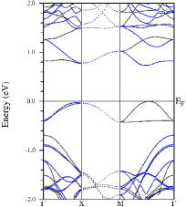
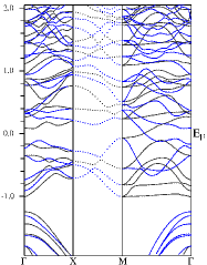
To understand the evolution of the electronic structure with number of VO2 layers, we focus primarily on the ferromagnetically aligned cases. Figure 1 shows the insulating band structure of the majority bands of the 5/1 system for FM alignment of the moments. This shape of the occupied bands, which is essentially that of the interfacial V atom band in the 5/3 system that we discussed in a previous paper,Pardo and Pickett (2009) underpins the understanding of the change in electronic structure as increases. One band is flat, or nearly so. The other of the pair has a sinusoid shape, although the end segments are not as quadratic as a true sinusoid. The two bands are degenerate at both and at M. Although these bands have a simple shape and would be expected to have a simple representation in terms of a tight-binding model, the two orientations of the VO2 octahedra in the rutile structure, and their lack of alignment of their natural axes with each other and with the cubic axes, preclude a straightforward representation by a tight-binding fit.
The gap of 0.8 eV present in this band structure can be attributed to its Mott insulating character; each V ion has a single orbital occupied. The occupied band width is 0.4 eV; all other majority states lie above the gap. For comparison, in the right panel of Fig. 1 we show the band structure of bulk VO2 in rutile structure, calculations being run with the same value of U. The V bands have the same shape and symmetry in both systems, but the bandwidth is reduced when the system is confined within TiO2 by a factor 2 for the occupied bands. The unoccupied bands in the multilayer system become complicated by the presence of Ti bands in the same energy region.
III.2 Bilayer VO2 slab
Increasing the thickness to two layers of VO2 (Fig. 2), both FM and AF couplings along the rutile c-axis can be studied, with the possibility of forming some precursor of the V-V dimers that occur in the dimerized monoclinic insulating low temperature phase of VO2.
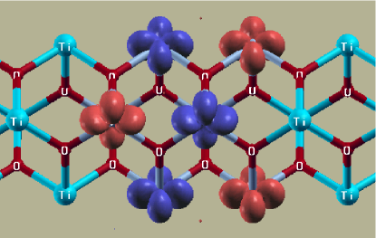
The 5/2 system is found to be an insulator, whether the V spin alignment is FM or AF. The energetically favored state, by 9 meV/V, has the two V atoms along a V chain (confined within 5 layers of TiO2) coupled antiferromagnetically. As found in our previous reportPardo and Pickett (2009) for the 5/3 system, the AF magnetic coupling leads to occupation of the orbital, with one pair of lobes directed along the c-axis, and forming the bonds along the rutile c-axis that can be seen in Fig. 2. The plot presents the spin-density isosurface and allows to visualize the orbital from the V4+ cation. This electronic structure is analogous to that of VO2 at low temperatures in the monoclinic dimerized phase, when it transitions to an insulating phase from the high temperature metallic rutile structure, except there is no dimerization. In VO2, the -bond along the chain and dimerization leads to a spin-singlet formation along the chain, resulting in a gap. In the case of multilayers of the thickness we consider (and even larger), the effect is not cooperative and no temperature-induced metalization is observed, as mentioned earlier.
The FM configuration of the 5/2 system is also insulating, but with a smaller band gap than in the AF case. To allow comparison of a systematic series of nanostructures, the band structure of the 5/2 system in a FM state along the rutile c-axis is included as the left panel of Fig. 3. When comparing this 5/2 system to 5/1 and 5/3, it can be seen how the bands that cross at the semi-Dirac point in the 5/3 system are approaching this energy region already in the 5/2 system. The FM configuration in this 5/2 case is not the lowest energy state, but it will be useful to see this reference band structure for understanding the origin of the semi-Dirac point Fermi surface that appears in the 5/3 and 5/4 ML systems, as shown in the middle two panels of Fig. 3. When comparing the 5/2 and 5/1 band structures, we see a new set of two V occupied bands, similar to those present in the 5/1 band structure, but with smaller bandwidth, and a corresponding reduction in the band gap of the full multilayer system can be observed. It is already clear that adding more layers of VO2 will lead to a metallic state.
III.3 Larger slabs, n= 3, 4, 5
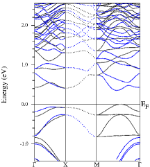
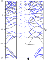

To provide the sequence up to, at, and beyond the semi-Dirac cases, Figure 3 shows the band structures of the (TiO2)5/(VO2)n system for values of from 2 to 5, from left to right. The alignment of energies in the various band structures presented in this figure was carried out using as a reference the O core state of the central oxygen in the (TiO2)5 layer. Using that reference, the occupied oxygen bands coming from the TiO2 layer are about the same position in energy, but the Fermi levels are not aligned. Nevertheless, the Fermi levels for = 3, 4, 5 are very nearly aligned, as would be expected once a metallic band structure is established.
As presented and discussed earlierPardo and Pickett (2009) the 5/3 system displays a very peculiar electronic structure not seen previously, consisting of a semi-Dirac dispersion around the point Fermi surface. The dispersion is massless (linear) along the (1,1) symmetry direction in k-space, and massive (quadratic) perpendicular to this direction at the semi-Dirac point. Such an unusual dispersion will lead to unexpected and unique physical properties,Banerjee et al. (2009) many of which remain to be studied. The origin of these peculiar Fermi points arises from a specific coupling of two bands related to the change in orbital ordering from the first unit cell to deeper cells. The change in orientation is the same in the 5/3 system as is pictured in the 5/5 system in Fig. 4. The interface V orbital always has the orientation shown in Fig. 2 for the 5/2 system. The orientation of the inner atoms is that of FM bulk VO2.

There are two pairs of bands, each with its own identifiable shape, that can be used to follow the formation and then the disappearance of the semi-Dirac band structure. The occupied pair in the 5/1 system was discussed above, and it appears twice in the 5/2 system, with centers displaced by about 0.4 eV. In the 5/3 system, a new pair of bands appears, which their character reveals to be a mixture of bands coming from V sites that are not at the interface. This pair of bands can be identified also in the 5/2 band structure, where they are the lowest pair of unoccupied states at the M point. These bands disperse in opposite directions from the M point, and the upper member crosses a band that is dispersing downward from above. This crossing gives rise to the semi-Dirac point. Since the crossing bands do not involve the interface V sites, and does not survive for more than four unit cells of VO2, the semi-Dirac phenomenon qualifies as a quantum confinement effect rather than an interfacial effect.
The occupied V orbital away from the interface is largely (but certainly not purely) a i orbital in a coordinate system that has in the plane. By symmetry, it is rotated by 90∘ for the other V ion in the cell. The distortion of the octahedron, and the two orientations of octahedra, in the rutile structure, make this orbital difficult to quantify in terms of the cubic orbitals, and also complicate the tight-binding representation of what appear to be simply dispersing pairs of bands. More comment on these orbitals are provided in Sec. V below. The two types of orbital occupation lead to the dispersion that finally produces the semi-Dirac point that pins the Fermi level.
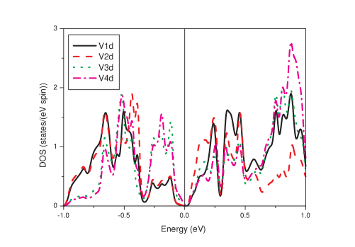
The 5/4 system is closely related to that of the 5/3 system. As in the 5/3 nanostructure, the FM configuration is lower in energy than an antiferromagnetic alignment along the rutile c-axis, by 57 meV/V. This disfavoring of AF ordering is consistent with the experimental observation that long-range dimer formation along the rutile c axis only occurs at VO2 thicknesses of several nm,Nagashima et al. (2007) enough to sustain a dimerization and structural cooperative distortion of the rutile-based lattice. Just as in the 5/3 system, this nanostructure has a half metallic zero-gap semi-Dirac structure. Figure 5 shows the partial density of states (DOS) of the four inequivalent V atoms, and the two central cells are different from those at the interface. For labeling the atom-projected DOS curves, the V atoms are named as V1-V2-V3-V4-V4-V3-V2-V1 from interface to interface along the rutile axis. The two innermost V atoms V3 and V4 contribute most to the DOS near the Fermi level, but very near the Fermi level a contribution from V2 (the more inner atom in the interfacial unit cell) becomes noticeable. The interfacial V1 atom has no contribution in either of the two bands that cross the Fermi level. Again, the semi-Dirac point is a confinement effect.
Increasing the thickness of the VO2 layer by adding a fifth layer to create the 5/5 multilayer, more bands appear at the Fermi level and the system reaches a metallic state, as shown in the right panel of Fig. 3. Thus the insulator-metal transition has completed for the thickness of the VO2 layer greater than 4 layers. The transition has proceeded through a very peculiar point-like Fermi surface stage that takes place only in the 5/3 and 5/4 systems. In the 5/5 system a crossing of two semi-Dirac bands occurs near the Fermi level along the - direction as in the 5/3 and 5/4 systems, but the system is metallic (normal) because several other bands also cross the Fermi level.
III.4 Band line-up across the interface
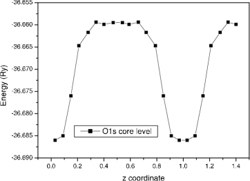
We use the 5/3 system to obtain the band line-up across the TiO2/VO2 interface, by referencing to the O core levels and then using the bulk electronic structures. The top panel of Fig. 6 shows that the O core level position converges (to the bulk value) within the TiO2 layer, but perhaps is not quite converged in the thinner VO2 layer. Still, this amounts to only a minor correction of the band alignments for an isolated interface. The resulting band line-up is shown in the lower panel of Fig. 6: the Fermi level of VO2 lies 1.0 eV above the bottom of the 3.0 eV gap of TiO2.
The behavior of the level energies provides insight into the healing length of the local potential away from the interface. In Fig. 6, the center of the TiO2 layer lies at =0.5 and the center of the VO2 layer at =1.0. The three central layers (of five total) of TiO2 have the same local potential, hence it is only the single TiO2 unit cell at the interface that experiences the effect of the interface on the potential. Only the cell at the interface is affected also in VO2, however, the energy difference between the two O ions in the cell is almost four times greater than on the TiO2 side. This result is consistent with a more polarizable ion compared to the ion, i.e. more screening on the VO2 side.

IV The semi-Dirac point
The band structure of the 5/4 system (third panel of Fig. 3) shows the appearance of pair of bands crossing just at the Fermi level, at only a single point along the plotted symmetry lines; i.e. a potential semi-Dirac point.Pardo and Pickett (2009); Banerjee et al. (2009) It lies along the direction, just as in the 5/3 case and in fact is similarly placed along the zone diagonal. This semi-Dirac-point low energy electronic structure therefore displays robustness: not only against variations in atomic positions and reasonable changes in the Coulomb repulsion U, but also against interfacial disorderPardo and Pickett (2009)and the more substantial change of adding one additional layer of VO2. For four VO2 layers, the V bands become narrower and have correspondingly more states in the same energy region, but the dispersion typical of the rutile metallic VO2 system remains. The other sets of bands, which come from the more internal VO2 layers, are very similar to the 5/3 case.
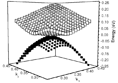
Since the band structure along symmetry lines does not necessarily determine what the dispersion is like (linear or quadratic) perpendicular to the line, it is necessary to check explicitly. Figure 7 shows a representation () of the two bands crossing the Fermi level in the 5/4 system, from which the parabolic energy dispersion in the perpendicular direction is evident. Hence the band crossing is indeed a semi-Dirac point, similar in all respects to the 5/3 system: electrons at the Fermi level behave as relativistic massless fermions along the zone diagonal and as massive particles along the perpendicular direction. The behavior of the system of semi-Dirac fermions for the 5/3 system will apply here as well.Pardo and Pickett (2009); Banerjee et al. (2009)
V Spin-orbit coupling
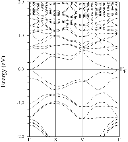
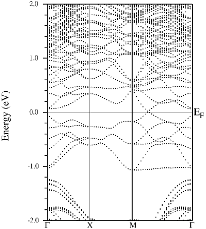
One important question that needs to be addressed is how spin-orbit coupling (SOC) affects the bands in the vicinity of the semi-Dirac point. At the Dirac point of graphene, it is known that SOC leads to a very small gap opening, destroying the perfection of the Dirac point.Kane and Mele (2005) However, the gap is so small that it probably has no measurable consequences. V atoms are somewhat heavier, so SOC should have a larger effect. There are in fact several interesting complications in this system.
First of all, this three-cell layer of VO2 is not only magnetic (unlike graphene), but it is half-metallic. The nearest minority bands that can be mixed by SOC into the majority bands at the semi-Dirac point are 1 eV away. Mavropoulos et al. Mavropoulos et al. (2004) have studied the effects of SOC in some intermetallic half metals, but without reporting on the size of any band gaps that might have resulted. They found that the amount of mixing (in terms of DOS) of minority into the majority band gap could range from 0.5% to a little more than 10%, depending on the size of the half metallic gap, the position of the Fermi level in the gap, etc. As a result of SOC, half metals are no longer strictly 100% half metallic due to spin mixing.
Second, our system is strongly two dimensional, and even the underlying rutile structure is anisotropic, especially in VO2 where the spin coupling along the -axis is strongly tied to the structural transition and insulator-to-metal transition.Booth and Casey (2009) However, unlike in graphene, there is a real underlying three-dimensional lattice in the present case. Thus different effects may be observed depending on the direction of the V spin moments. Thirdly, the two bands that cross at the semi-Dirac point have different weights on distinct V ions, viz. mostly V2 ions for one, V3 ions for the other. This will affect the magnitude of the coupling, since SOC is a local (single atom) interaction.
The SOC operator in the Kohn-Sham Hamiltonian, 22 in spin space, is
| (1) |
where etc. We consider the two distinct cases of direction of the spins, and we are interested in the majority (spin “up”) bands. We focus on the coupling only between the two bands () near the semi-Dirac point. In each case we quantize (hence ) along the direction of the V spin moment. Then the matrix element directly coupling the two bands becomes (suppressing the index)
| (2) |
The band-diagonal matrix elements, giving simple band shifts for the two bands, will not impact this gap opening question. The remaining coupling arises from second (and higher) order terms involving the spin-down conduction band 1 eV and higher in energy, leading to corrections that are at a maximum /1 eV) which will be very small, and we do not consider these corrections further (though they are included in the band structure calculations). From the above equation, band mixing will give a gap .
Case 1. along the axis. This is the calculated ground state, with energy about 10 meV/V lower than for polarization in the plane. In this case, the calculated band structure shows that the semi-Dirac point at the Fermi level persists (right panel of Fig. 8). The calculated value of orbital moment is 0.04 for each V ion, a fairly typical moment for a atom in a magnetic material. The fact that the band crossing still occurs indicates that SOC does not interfere with the difference of symmetries of the two bands along the line that allows them to cross (without SOC); the matrix element vanishes due to the differing symmetry of the bands.
Case 2. along the axis. In this case, a substantial gap eV is observed (left panel of Fig. 8) to open up at the former location of the semi-Dirac point. The V orbital moments that result, which are six separate values since the V ions all become inequivalent, are as high as 0.2 inside the muffin-tin sphere. The largest value occurs for the orbital whose local axis is parallel to and is ready-made to respond with an orbital moment along the axis. The change in symmetry of the system when the moment lies in the plane results in band mixing, i.e. the matrix element no longer vanishes due to symmetry. The unexpectedly large SOC-induced gap is connected with the large orbital moment.
Another observation from Fig. 8 can be noted. In the left panel, after the gap has opened due to SOC, the upper two occupied V bands lie in energy roughly where they were without SOC (right panel). The two pairs of V bands at lower energies, however, have moved lower in energy by 0.4 eV, an unusually large shift for an effect of SOC. We attribute this shift to the large orbital moments that are induced when the spin lies in the plane.
That the subshell provides a representation for L=1 (not L=2) orbital moments has long been known.Abragam and Bleaney (1970); Stevens (1953); Goodenough (1968); Lacroix (1980); Pickett and Eschrig (2007) Fairly recently several cases have come to light in which orbital moments can actually be quenched within the shellKhaliullin and Maekawa (2000) by structure-induced or spontaneous symmetry lowering, or an orbital moment can compensate a spin moment and prevent orbital ordering.Lee and Pickett (2007) Other more complicated orders may appear in Sr2VO4, where the effects of spin-orbit may lead to a hidden octupolar order with vanishing expectation values for both L and S.Jackeli and Khaliullin (2009) In the V4+ system studied in this paper, an unexpectedly large orbital moment is induced by the spin moment for the orbital.
VI Conclusions
In this paper we have presented electronic structure calculations on the multilayer system (TiO2)m/(VO2)n, to study the effects of nanostructuring a correlated material like VO2 that in the bulk undergoes a metal-insulator transition, sandwiched by a band insulator like TiO2. The system provides an example of a - interface with no polar discontinuity, so many of the questions that exist for other oxide heterostructures are moot here. By increasing the VO2 layer thickness, the multilayer shows a metal-insulator transition. For n 5 layers, the system becomes metallic, being insulator for n= 1 and 2. The system is, experimentally, susceptible to the recovery of the bulk properties typical of VO2 for n 15 (specifically, the temperature-induced structural transition). We have studied values of n significantly smaller, where the effects of quantum confinement can be important. The metal-insulator transition in the multilayer occurs through a semi-Dirac point phase for n= 3 and 4, in which the Fermi surface is a sngle point, around which the electrons behave as massless along the zone diagonal in k-space and as massive fermions along the perpendicular direction. In previous papers, we analyzed the semi-Dirac state for the n= 3 case, finding it to be robust against interfacial disorder and a reasonable range of U values. In this paper, we observe that it persists also for n = 4, hence showing some (limited) robustness to the VO2 thicknesses. We point out that spin-orbit coupling does not destroy this semi-Dirac point, where the spin lies along the rutile axis. The ground state has small orbital angular moments, hence the changes in the band structure introduced by spin-orbit coupling are very small and the semi-Dirac survives spin-orbit coupling.
VII Acknowledgments
We acknowledge useful interactions with S. Banerjee and R. R. P. Singh during the course of this work. This project was supported by DOE grant DE-FG02-04ER46111 and through interactions with the Predictive Capability for Strongly Correlated Systems team of the Computational Materials Science Network and a collaboration supported by a Bavaria-California Technology grant. V.P. acknowledges financial support from Xunta de Galicia (Human Resources Program).
References
- Morin (1959) F. J. Morin, Phys. Rev. Lett. 3, 34 (1959).
- Goodenough (1971) J. B. Goodenough, J. Solid State Chem. 3, 490 (1971).
- Muraoka and Hiroi (2002) Y. Muraoka and Z. Hiroi, Appl. Phys. Lett. 80, 583 (2002).
- Strelcov et al. (2009) E. Strelcov, Y. Lilach, and A. Kolmakov, Nano Letters 9, 2322 (2009).
- Wei et al. (2009) J. Wei, Z. H. Wang, W. Cheng, and D. H. Cobden, Nat. Nanotech. 4, 420 (2009).
- Pentcheva and Pickett (2006) R. Pentcheva and W. E. Pickett, Phys. Rev. B 74, 035112 (2006).
- Siemons et al. (2007) W. Siemons, G. Koster, H. Yamamoto, W. A. Harrison, G. Lucovsky, T. H. Geballe, D. H. A. Blank, and M. R. Beasley, Phys. Rev. Lett. 98, 196802 (2007).
- Park et al. (2006) M. S. Park, S. H. Rhim, and A. J. Freeman, Phys. Rev. B 74, 205416 (2006).
- Pentcheva and Pickett (2008) R. Pentcheva and W. E. Pickett, Phys. Rev. B 78, 205106 (2008).
- Willmott et al. (2007) P. R. Willmott, S. A. Pauli, R. Herger, C. M. Schleputz, D. Martoccia, B. D. Patterson, B. Delley, R. Clarke, D. Kumah, C. Cionca, et al., Phys. Rev. Lett. 99, 155502 (2007).
- Nagashima et al. (2007) K. Nagashima, T. Yanagida, H. Tanaka, and T. Kawai, J. Appl. Phys. 101, 026103 (2007).
- Hohenberg and Kohn (1964) P. Hohenberg and W. Kohn, Phys. Rev. 136, B864 (1964).
- Schwarz and Blaha (2003) K. Schwarz and P. Blaha, Comp. Mat. Sci. 28, 259 (2003).
- Sjöstedt et al. (2000) E. Sjöstedt, L. Nördstrom, and D. J. Singh, Solid State Commun. 114, 15 (2000).
- Anisimov et al. (1991) V. I. Anisimov, J. Zaanen, and O. K. Andersen, Phys. Rev. B 44, 943 (1991).
- Ylvisaker et al. (2009) E. R. Ylvisaker, W. E. Pickett, and K. Koepernik, Phys. Rev. B 79, 035103 (2009).
- Biermann et al. (2005) S. Biermann, A. Poteryaev, A. I. Lichtenstein, and A. Georges, Phys. Rev. Lett. 94, 026404 (2005).
- Tomczak and Biermann (2007) J. M. Tomczak and S. Biermann, J. Phys.: Condens. Matter 19, 365206 (2007).
- Haverkort et al. (2005) M. W. Haverkort, Z. Hu, A. Tanaka, W. Reichelt, S. V. Streltsov, M. A. Korotin, V. I. Anisimov, H. H. Hsieh, H. J. Lin, C. T. Chen, et al., Phys. Rev. Lett. 95, 196404 (2005).
- Pardo et al. (2008) V. Pardo, S. Blanco-Canosa, F. Rivadulla, D. I. Khomskii, D. Baldomir, H. Wu, and J. Rivas, Phys. Rev. Lett. 101, 256403 (2008).
- Pardo and Pickett (2009) V. Pardo and W. E. Pickett, Phys. Rev. Lett. 102, 166803 (2009).
- Banerjee et al. (2009) S. Banerjee, R.R.P. Singh, V. Pardo, and W. E. Pickett, Phys. Rev. Lett. 103, 016402 (2009).
- Kane and Mele (2005) C. L. Kane and E. J. Mele, Phys. Rev. Lett. 95, 226801 (2005).
- Mavropoulos et al. (2004) P. Mavropoulos, K. Sato, R. Zeller, P. H. Dederichs, V. Popescu, and H. Ebert, Phys. Rev. B 69, 054424 (2004).
- Booth and Casey (2009) J. M. Booth and P. S. Casey, Phys. Rev. Lett. 103, 086402 (2009).
- Abragam and Bleaney (1970) A. Abragam and B. Bleaney, Electron paramagnetic resonance of transition ions (Clarendon Press, Oxford, 1970).
- Stevens (1953) W. H. Stevens, Proc. Royal Soc. London A 219, 542 (1953).
- Goodenough (1968) J. B. Goodenough, Phys. Rev. 171, 466 (1968).
- Lacroix (1980) C. Lacroix, J. Phys. C 13, 5125 (1980).
- Pickett and Eschrig (2007) W. E. Pickett and H. Eschrig, J. Phys.: Condens. Matt. 19, 315203 (2007).
- Khaliullin and Maekawa (2000) G. Khaliullin and S. Maekawa, Phys. Rev. Lett. 85, 3950 (2000).
- Lee and Pickett (2007) K. W. Lee and W. E. Pickett, EPL 80, 37008 (2007).
- Jackeli and Khaliullin (2009) G. Jackeli and G. Khaliullin, Phys. Rev. Lett. 103, 067205 (2009).