Terahertz-field induced tunneling current with non-linear effects in a double quantum well coupled to a continuum
Abstract
We have theoretically investigated the tunneling current induced by a terahertz (THz) field applied to an asymmetric double quantum well. The excitation couples an initially localized state to a nearby continuum of extended states. We have shown that the calculated current has similar features as those present in the optical spectra, such as interference effects due to the interaction between the continuum and the localized states, in addition to many-photon transition effects. The induced current is calculated as a function of the intensity of the THz field. A second THz field is used to yield non-linear processes, useful to control the interference effects. We believe that part of the issues studied here can be usefull for the integration of novel switching mechanisms based on optics (THz) and electronic current.
pacs:
71.35Pq, 73.21.La, 78.55Cr, 78.67.HcI Introduction
Fast switching mechanisms are desirable for a number of applications, including in quantum information processing. A limitation on the time-scale performance of these mechanisms is usually a consequence of the prevalence of incoherent processes, such as the slow dynamics of population decay. One possible way to overcome this problem is to restrict the processes to the faster quantum coherent dynamics, as in the case studied by Wu et al.wu in which a scheme was proposed for an all-optical switching mechanism based on the virtual excitation of excited states by two independent terahertz (THz) fields.
The system investigated by Wu et al.wu is a double quantum well separated by a thin barrier from a continuum of states (see Fig. 1). By exciting this system with a THz (probe) field one sets the ground state (which is occupied by electrons from a nearby reservoir) in resonance with two almost degenerate excited states, both coupled to the continuum. This coupling creates a Fano-like interferencefano which manifests itself as a strong suppression of the field absorption. As a result, the probe THz spectra show two asymmetric peaks with an almost zero absorption in between the peaks.schmidt ; faist When a second (switch) THz field is used, with a frequency that sets the resonance between the pair of excited states to a further excited state, there occurs a substantial modification of this interference. In this way, one can control the probe absorption with the switch field,harris noticeably when the inference effect is intense.
The novelty of the proposed all-optical switching device is in the fact that it deals with virtual excitation of the highly energetic state, therefore it can be quickly switched on and off. The calculations to support the proposed model was done with a set of coupled Maxwell-Schrödinger equations for the occupations of the quantum levels and for the exciting THz fields.wu The focus of the attention was on the temporal evolution of the probe transmission under the control of the switch field.
In the present work we obtain similar results looking at the THz-field–induced tunneling current. We have solved numerically the time evolution of a one-electron state, initially localized in the asymmetric double well, in the presence of an applied THz field pulse (probe). Interference effects due to interaction with the continuum are observed in the tunneling current as well as many-photon processes. A second field (switch) can be used to control this interference, thus opening the possibility to create switching mechanisms, which in the present case have a signature in the tunneling current. This may be usefull for the integration of optical and electronic schemes in a switching mechanism.
II Theory
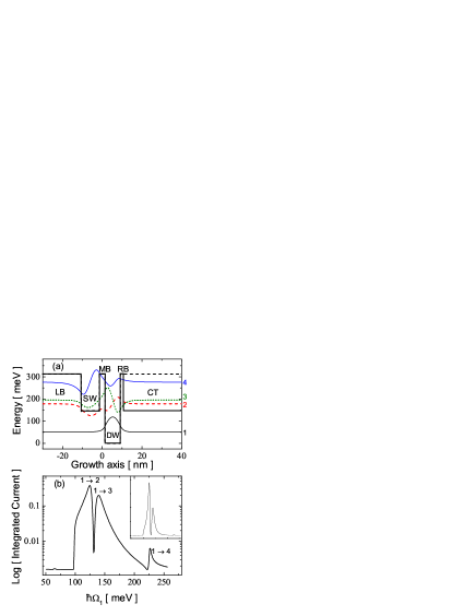
The system investigated is an asymmetric double quantum well which is separated from a continuum of states by a thin potential barrier (RB), as depicted in Fig. 1. An electron in the ground state, localized in the deeper quantum well (DW), is excited by the probe field and may tunnel to the continuum. The current associated with this process is calculated from the time evolution of the single initially localized state that the electron occupies at . This is done within the effective-mass approximation for an one-electron problem in the conduction band. A second (switch) oscillating field can be used to control this tunneling current.
The problem is solved numerically using the following one-dimensional hamiltonian
| (1) | |||||
where is the electron effective mass, assumed uniform throughout the system, is the potential due to the material band-offsets, and () is the envelope of the applied probe (switch) electric field oscillating with frequency () and polarized along the direction. represents a possible relative phase between the fields. The probe and switch fields are assumed as pulses, with envelopes in the form of Gaussians, and is the delay between the two pulsed fields.
The ground state of the system is calculated first without the application of THz fields. As mentioned, the ground state is localized on the right-hand-side well of the structure which has the deepest potential (DW). The numerical method for this calculation uses imaginary-time propagation within a split-operator approach review ; degani . The ground state is used as the initial state to be advanced in time under the full hamiltonian Eq. (1) by performing the operation in small time increments :
| (2) |
Details of the numerical procedure are given in Refs. review, ; degani, .
With the application of a THz field, which can have the field frequency and intensity varied, the initial state can be coupled to excited states to create a particle current flowing to both sides of the structure. In the present work the exciting fields are chosen with energy that is sufficient to excite current only towards the right side of the system. The current is calculated at a given point in the (right-hand side) region of the continuum by the expression
| (3) |
from which the integrated current is calculated
| (4) |
Since the numerical method employed uses hard-wall boundary conditions, meaning vanishing wavefunctions at the boundaries of the system, these currents can be reflected at the system boundaries and produce interference effects. To avoid these effects in the calculation of the field-induced current, a spatially large system is used with the inclusion of imaginary-potential barriers on its edges. These regions act as damping barriers and minimize wavefunction reflections. The important parameters to be set for these damping barriers are basically their spatial extent and their potential heights. Limiting values for these parameters are given in the work of Neuhasuer and Baerneuhasuer and they depend on the energy of the electron impinging on the barrier. Since our electron current are the result of THz-photon absorption, the energy of the electron contributing to the current depends on the exciting field frequency. This makes the calibration of these parameters a little tricky, yet it is still possible to considerably reduce unwanted reflection-effects in this way.
III Results and discussion
The asymmetric double well system investigated is as shown in Fig. 1, and consists basically of a one-dimensional problem with the band-offset energies taken from the materials GaAs/AlxGa1-xAs that make up real systems. The effective mass and dielectric constant used are those of GaAs, namely , being the bare electron mass, and . The band-offset energies are given as a function of the Al concentration by the following equation,concentration
| (5) |
The regions of the structure will henceforth be labeled, starting on the left side as: left barrier (LB), shallower well (SW), middle barrier (MB), deeper well (DW), right barrier (RB), and continuum region to the right (CT).
The thickness of the barriers and wells, inasmuch as their potential heights (i.e. the Al concentration ) were chosen carefully in order to have a ground state (state-1 in Fig. 1) localized in the deepest well with the next two excited states (state-2 and -3) forming almost a doublet, and a fourth state (state-4) still bound to the double well. In fact, all these excited states are virtual bound states, since the presence of the continuum (CT) allows for only one truly bound state (the ground state). An additional characteristic was desired, namely, that the energy separation between the doublet of excited states (state-2 and 3) and the upmost higher energy state (state-4) should be smaller than the energy difference between the state-1 and the onset of the continuum. This warrants that exciting fields with frequencies capable of coupling states-2 and 3 with state-4 will not create currents due to transitions from the ground state at DW to the continuum (CT).
A set of system parameters attending the above specifications is found:
-
•
LB: Al0.4Ga0.6As, 240 nm thick;
-
•
SW: Al0.2Ga0.8As, 9 nm thick;
-
•
MB: Al0.4Ga0.6As, 3 nm thick;
-
•
DW: GaAs, 7.7 nm thick;
-
•
RB: Al0.4Ga0.6As, 1.5 nm thick;
-
•
CT: Al0.2Ga0.8As, 750 nm thick.
To help finding this set of parameters, RB height was first taken equal to the LB (both with Al concentration =0.4). In this case the four states are truly bound states with energies: E1 = 50 meV, E2 = 180 meV, E3 = 190 meV and E4 = 270 meV, with respect to the bottom of DW (the GaAs well). When CT is set with =0.2, a continuum of states is formed in the far right region and affects these energies. Next we discuss how this can be seen from the THz-induced current calculations.
To calculate the field-induced current two damping barriers at the system edges were used. A 30-nm thick damping barrier was defined on the far left side of LB and similarly a 40-nm thick barrier was placed on the far right side of CT. Both imaginary barriers had a potential of approximately 50 meV. The particle current (Eqs.(3) and (4)) were calculated in a position just before the damping barrier in CT.
In Fig. 1(b) the integrated current induced by the probe field (switch is off) is shown as a function of the probe frequency (energy) in a logarithmic scale. The inset shows the same but in a linear vertical scale. It is observed that for probe energies less than 98 meV there is almost zero current in view of the fact that the THz photon energy is not sufficient to excite the ground state to at least the onset of the continuum in CT. Above this limiting energy the current grows up to finite values and manifests two strong peaks about 127 meV and 143 meV, and a weaker peak at 225 meV. These peaks in the spectrally resolved current are related to the transitions induced by the THz field from the ground state to the (virtual) excited states (states-2, -3, and -4) followed by tunneling to the continuum (see Fig. 1(b)). It is interesting to note the similarity of this spectra for the induced current with the optical spectra for the intersubband transitions calculated by Wu et al.wu . Like the optical spectra, the induced current (or photocurrent) spectra shows two peaks with a strong depletion in between resulting from interference effects with the nearby continuum, that is, a Fano-like effect. This strong suppression of current between the two peaks can be manipulated to create switching devices with fast responses, as pointed out by Wu et al.wu in their study for the optical case. Here, we explore similar effects however looking at the photocurrent generated in the process. Before turning the switch field on, we further discuss the effects of the probe field on the induced current.
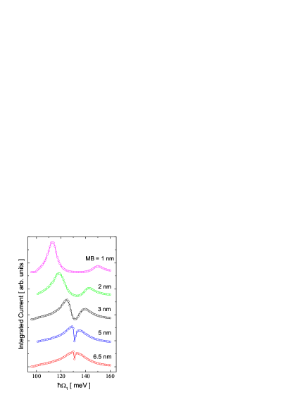
In Fig. 2 the induced current is shown for systems with different thicknesses of the middle barrier MB, with the spectra focused on the two stronger peaks related to the transitions 12 and 13. The effect of increasing the thickness of MB is to decouple the two quantum wells. As MB becomes wider, the doublet weakens and the (virtual) excited states become more independently localized in different quantum wells. State-2, mostly localized in the SW, contributes little to the current since the transition 12 is weakened with the decrease of both the spatial overlap between states 1 and 2, and the probability of tunneling to the continuum. This is seen in Fig. 2 with the merging of the two peaks in a one (13). In this process, the interference effects with the continuum are retained.
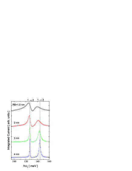
In Fig. 3 the coupling with the continuum is investigated by varying the thickness of the right barrier RB. As RB becomes wider, the states in the double well are less affected by the continuum. It is then observed that the peaks become sharper, indicating longer lifetimes (lesser couplings to the continuum), and it is also observed a large splitting between the peaks, since the states effectively become more localized in the double well region. Note that for large RB thicknesses (near 4 nm in Fig. 3), the energies of the two peaks tend to the values expected for the double well system in the absence of the continuum.
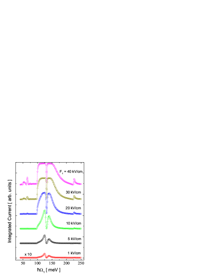
Next, the intensity of the probe field is varied, with the result shown in Fig. 4. For moderate intensities 10 kV/cm the two peaks for the transitions 12 and 13 dominate the spectrum. For stronger intensities the peak for the transition 14, at the higher energy side of the spectrum, has its amplitude increasing linearly with the field intensity. For the lower energy side of the spectrum, a double peak appears whose amplitude increases superlinearly with the field’s intensity. This part of the spectrum is not allowed for one-photon transitions due to energy conservation. Hence, this peak is attributed to a two-photon process for the transitions 12 and 13. The superlinear growth of this double peak and its energy in the spectrum (half of that permitted for the one-photon process) strongly supports this interpretation. Another feature seen in Fig. 4 is a saturation effect for energies around the 12 and 13 transitions. The relatively small values for the intensities of the fields that produce such a saturation are spurious and follows from the single-electron physics used to calculate the current. For larger fields, and strong transition rates, a single-electron is completely ionized by the THz field, causing the integrated current to saturate. For an actual system with electrons provided by dopant impurities, the saturation (complete ionization) is expected to occur at higher field intensities.
When a second (switch) field is used, the spectrum is modified especially in the region between the transitions 12 and 13 where interference with the continuum strongly supresses the induced current. This is due to the absorption of an additional photon that excites the transition from states 2 and 3 to the higher energy state-4. Figure 5 shows the spectra for a system with barriers’ thicknesses of 3 nm and 1.5 nm for MB and RB, respectively, for a probe intensity F1= 10 kV/cm and a switch field intensity F2 = 20 kV/cm. The two pulses have the same time spams (2 ps) and phases and have zero delay between them [=0 and =0 in Eq. (1)]. The frequency of the switch is varied slightly around the energy difference between the states-(2,3) and state-4. Note that the switch field alone does not induce current for these frequencies since the corresponding photon energy is smaller than the energy difference between the ground state and the onset of the continuum, which is 98 meV. The system parameters were carefully chosen to yield such a behavior.
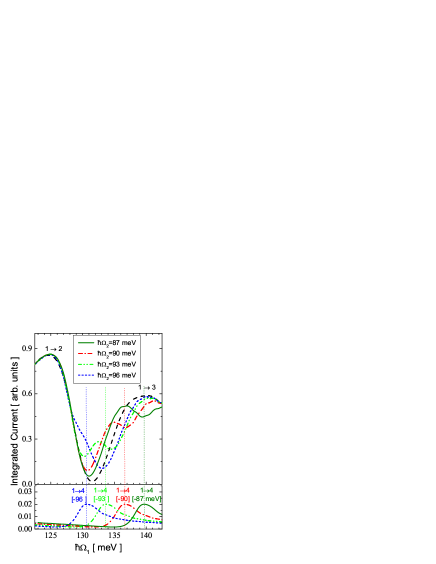
In the lower panel of Fig. 5 the peak corresponding to transition 14 is seen to be redshifted by exactly the switch field energy . It shows that the part of the spectrum (upper panel) that is affected by the switch is the one in the energy range that matches an additional transition to the state-4 by the absorption of a switch photon. The effect of the switch can be either weakening an existing current by further excitation to the state-4 (as in Fig. 5 for = 87 meV) or enhancing an otherwise suppressed current (as it is the case for = 93 meV) by modifying the interference with the continuum. This latter case was explored by Wu et al.wu as a possible all-optical switching mechanism, since the switch field strongly modifies the optical absorption of the probe field. We observe similar effects, not on the optical absorption, but instead on the induced current, meaning that the optical switching mechanism can have a similar signature on its photocurrent. It is observed, for a probe field with frequency set at the zero current ( 132 meV) and a switch field with 93 meV, that neither of the two fields alone suffices to induce current, yet when they are simultaneously present there is an appreciable current induced (that is, a current that is larger than that originated in two-photon processes). This pattern can be used in a logic gate integrating optics and electronics.
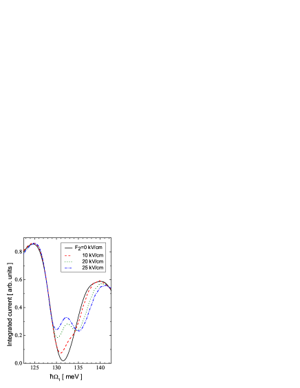
Finally, in Fig. 6 the effect of the switch-field’s intensity on the induced current is shown for a probe intensity F1 = 10 kV/cm. As it would be expected, increasing the switch intensity enhances the switching effects just described. We have obtained results similar to the ones shown in Fig. 6 by increasing the delay time between the two pulses [ in Eq. (1)] , that is, the delay effectively lowers the intensity of the switch field that is necessary to produce the desired switching effect. No changes were observed in the integrated current when varying the relative phase in Eq. (1).
In conclusion, the photocurrent induced by THz fields was investigated theoretically for a asymmetric double quantum well structure. The system parameters were chosen to have two excited (virtual) states forming a doublet which interacts with a nearby continuum yielding an almost zero induced current for probe field frequencies between the energies of the states in the doublet. A second (switch) field was used to modify the interference with the continuum by coupling the doublet to a higher excited state. The resulting current could be used as a logic gate integrating optics and electronics. Besides this two-field (probe/switch) investigation, the induced current was studied with varying system parameters, and also for nonlinear effects, such as the two-photon absorption for intense fields. Although the study contemplated a simple one-dimensional model, similar trends should be expected for electrons bound, for example, in a quantum dot and interacting with a nearby a continuum, such as a wetting layer. The THz fields were assumed as pulses and the initial state evolved in time was a single electron only for convenience in the numerical calculations. More realistic conditions in actual situations where such logic mechanism would operate, for example in continuous excitation, with the presence of many electrons, or under large bandwidth field excitation may enrich the problem but the trends found here can be the starting point for future investigations of the induced photocurrent.
ACKNOWLEDGMENT
MZM, MHD, and PFF gratefully acknowledge financial support from Programa Institutos Nacionais de Ciência e Tecnologia and Conselho Nacional de Desenvolvimento Científico e Tecnológico - CNPq/MCT. MHD thankfully acknowledges financial support from Dhiminsky ATA.
References
- (1) Jin-Hui Wu, Jin-Yue Gao, Ji-Hua Xu, L. Silvestri, M. Artoni, G. C. La Rocca, and F. Bassani Phys. Rev. Lett. 95, 057401 (2005). Phys. Rev. A 73, 053818 (2006).
- (2) U. Fano, Phys. Rev. 124, 1866 (1961).
- (3) H. Schmidt, K. L. Campman, A. C. Gossard, and A. Imamoglu, Appl. Phys. Lett. 70, 3455 (1997).
- (4) J. Faist, F. Capasso, C. Sirtori, K. W. West and L. N. Pfeiffer, Nature (London) 390, 589 (1987). 2180 (2005).
- (5) S. E. Harris and Y. Yamamoto, Phys. Rev. Lett. 81, 3611 (1998).
- (6) D. Neuhasuer and M. Baer, J. Chem. Phys. 90, 4351 (1989). 2180 (2005).
- (7) M. H. Degani and M. Z. Maialle, to appear in J. Comput. Theor. Nanosci. (2009).
- (8) M. H. Degani, G. A. Farias, and F. M. Peeters, Phys. Rev. B 72, 125408 (2005).
- (9) H. J. Lee, L. Y. Jurovel, J. C. Wolley, and A. J. Springthorpe, Phys. Rev. B 21, 659. (1980).