Magnetic bubbles in FePd thin films near saturation
Abstract
The structure of domain walls delimiting magnetic bubbles in L10 FePd thin layers is described on the basis of Lorentz transmission electron microscopy (LTEM) and multiscale magnetic simulations. Images obtained by high resolution LTEM show the existence of magnetization reversal areas inside domain walls, called vertical Bloch lines (VBL). Combining these observations and multiscale simulations on various geometries, we can identify the structure of these VBL, notably the presence or not of magnetic singularities.
I Introduction
FePd alloys with L10 structure deposited in thin layers have attracted much attention because of their very high perpendicular anisotropy, which is a key property for magneto-optical recording and for high density magnetic storage. Recently, alloys with a perpendicular anisotropy have been used in spin-valves, where they are used as the polarizer and as the free layer that should be reversedSeki et al. (2006). It has been shown that in such devicesSeki et al. (2008) or in magnetic tunnel junctions, the reversal of the free layer occurs through the nucleation of a reversed domain followed by the propagation of a domain wall.
Near the saturation, the band domain structure in FePd layers transforms into a lattice of magnetic bubblesHubert and Schäfer (1998), which remains stable at high fields. In some bubbles the Bloch-like walls have different polarities, separated by segments called vertical Bloch lines (VBL). In the present work we analyze the role of VBL on the shape of these magnetic bubbles.
VBL were much studied in the 1980s in garnets, both experimentally and numerically. Typical parameters for these garnets are , and , so that the domain wall width is . This large value, compared to the domain wall width in FePd of around 8 nm, makes possible the optical observation of domain walls and VBLThiaville and Miltat (1990). In FePd, a higher resolution is necessary to probe the sample, which can be reached by Lorentz transmission electron microscopy (LTEM). Extensive analytical and numerical studies have also been performed in VBL in garnetsSlonczewski (1974); Hubert (1974); Nakatani and Hayashi (1988); Miltat et al. (1989). Given the high value of the quality factor , a common assumption in the models is , which notably permits to use a local approximation of the demagnetizing field and thus simplifies the calculations. This assumption is a priori not valid in the case of FePd, which exhibits smaller values of of the order of 1.6.
In the present work we performed high resolution imaging of domain walls in magnetic bubbles in FePd thin layers, using Lorentz microscopy, to highlight their magnetic configuration. In particular we describe the influence of VBL on the shape of the bubbles. We also show the results of multiscale simulations that provide an explanation for these observed shapes.
II Observation of magnetic bubbles in FePd thin film
Lorentz microscopy is now a well established method that enables magnetic imaging with a resolution better than ten nanometers. The simplest mode of LTEM is the observation of the overlapping of electrons experiencing different Lorentz forces in magnetic domains. The contrasts obtained by simply defocalizing the lens used for imaging are called Fresnel contrasts Chapman (1984). In a classical in-plane magnetization configuration, Fresnel contrasts appear on the domain walls position due to the overlapping of electrons coming from two opposite domains. In the particular case of FePd, where magnetization is mainly out-of-plane, the contrasts can be obtained by tilting the sample Aitchison et al. (2001). This enables the magnetization inside the domain to act on the electron beam and to produce traditional Fresnel contrasts located on the domain walls. Otherwise contrasts can be produced by the domain walls themselves if the layer is thick enough and if the amount of in-plane magnetization in the wall is large enoughMasseboeuf et al. (2009) (i.e. to reach the LTEM sensitivity of about 10 nm.T). This was the case for our samples, so we have performed Fresnel observations of Bloch walls without tilting the FePd layers. The microscope used in these observations was a JEOL 3010 fitted in with a Gatan imaging filter for contrast enhancementDooley and De Graef (1997). The images displayed in this letter have been also filtered by a Fourier approach to enhance the contrasts localized on the domain walls. The magnetization was performed using the objective lens, calibrated with a Hall Probe. The sample was prepared by Molecular Beam Epitaxy on MgO [001] substrate. The magnetic stacking is decomposed in two layers: a “soft” layer of 17 nm FePd2 having a vanishing anisotropy is deposited before a 37 nm-L10 layer of FePd. Details can be found in Ref. Masseboeuf et al., 2008. The sample was prepared for TEM observation with a classical approach: mechanical polishing and ion milling.

Fig. 1 shows two different areas of the foil during the magnetization process. We observe couples of black and white contrasts corresponding to the Bloch wallsMasseboeuf et al. (2009). These pictures have been obtained for increasing applied fields. We should notice that upon 500 mT the quality of the images decreases due to the action of the objective lens on the image formation. Nevertheless it is possible to follow the shape of the domains during the magnetization process (enhanced here by Fourier filtering). We observe in both cases that a magnetic domain collapses to a bubble state. Attention can thus be paid on the chirality of the Bloch wall. The chirality (sense of the magnetization inside the Bloch wall) is directly linked to the Fresnel contrast: the wall chirality of a black/white contrast and the chirality of a white/black contrast are opposite. Knowing this, the observation of the two magnetic bubbles presented in the right images of Fig. 1 gives some information on the magnetization inside the domain walls of the bubbles. The first bubble presents a continuous domain wall, swirling all around the bubble, whereas the other one exhibits two different parts with the same magnetization orientation. In the latter configuration, the magnetization inside the domain wall experiences two rotations of 180∘ localized at the top and the bottom of the bubble. These switching areas are known as vertical Bloch lines (VBL). One can notice the main difference in the two bubble shapes: the first one is almost round while the second bubble seems to be slightly elongated along the vertical direction.
To confirm the role of VBL on the bubble shape, we have thus simulated the inner structure of domain walls containing VBL.
III Simulation of domain walls with vertical Bloch lines
The numerical simulation of magnetic bubbles is not a tractable problem with standard codes. Indeed it requires to handle large systems whose size is related to the size of the bubbles, but with regions where the magnetization varies rapidly in space, such as domain walls and all their substructures. Considering all regions with the same level of refinement is clearly not well adapted to such a multiscale problem and leads to a high computational effort. The same level of accuracy can be reached with a coarser mesh in uniformly magnetized regions.
In this work we used a multiscale code (Mi_Magnet) based on an adaptive mesh refinement technique, as well as on a mixed atomistic-micromagnetic approach, to achieve both precision and computational efficiencyJourdan et al. (2008). Given the large size of the systems we envisage here, the code was only used in its micromagnetic mode. It has been recently shown that micromagnetic calculations can be applied to singularities appearing in VBL, called Bloch Points (BP)Thiaville et al. (2003). In all calculations the mesh step is kept lower than half the exchange length.
Parameters are chosen in agreement with experimental measurementsGehanno et al. (1997): the saturation magnetization, anisotropy constant and exchange stiffness are , , and . With such parameters, the exchange length is .
Two types of computations have been carried out. First we investigate the properties of a straight domain wall containing a VBL. Secondly we study the role of VBL on the shape of the magnetic bubbles in FePd layers.
III.1 Vertical Bloch lines in straight domain walls
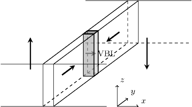
The system used here contains a domain wall with a single VBL (Fig. 2). The lateral size of the system is and the thickness of the layer is varied between 11.3 to 37.6 nm. No periodic boundary conditions are used, because this would involve a second VBL along and a second domain wall along . A view of such a system is given in Fig. 3.
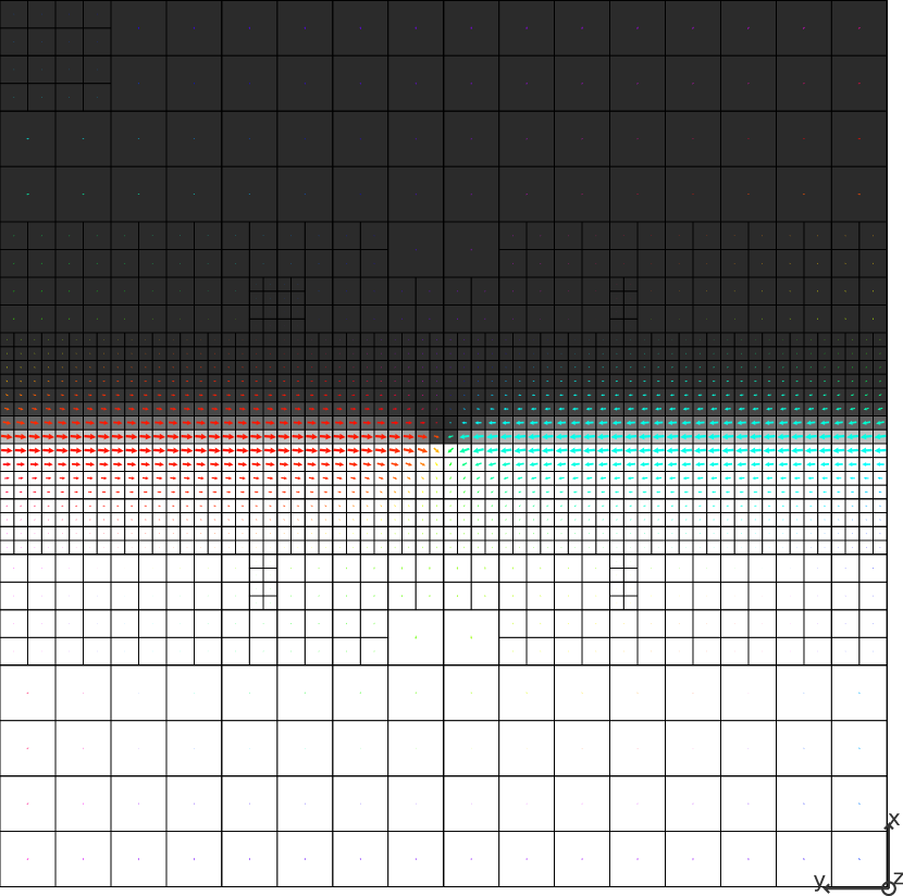
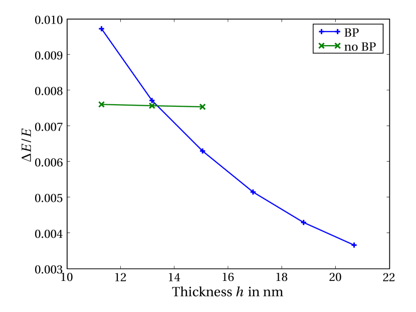
For all the values of the thickness that we envisage, we consider configurations with and without a BP (Fig. 4 and 5). The configuration without a BP can be stabilized only for a thickness lower than 15 nm and becomes energetically favorable below a critical thickness of around 13 nm (Fig. 6). For thicknesses larger than 15 nm, well defined Néel caps are present due to the dipolar field created by the domains and a BP nucleates on the surface where the magnetization rotates of nearly 360∘ (Fig. 5, at ). It must be noted that the critical thickness is around , which is significantly lower than the value found by a variational methodHubert (1976). Indeed this method, based on a local approximation of the dipolar field, is well justified if but does not hold in our case.


An interesting feature of the domain wall containing a VBL without a BP is the so-called buckling of the magnetization near the line. This buckling was already described in garnets, where it was ascribed to the diminution of the magnetic charges created by the variation of the magnetization in the direction orthogonal to the wallMiltat et al. (1989) (which we note here). These charges are called charges or dipolar charges, in analogy with orbitals, because positive charges are associated with negative charges.
Analytical models, based on the assumption , and two dimensional simulations, predict a much smaller value of the bucklingMiltat et al. (1989). Given our material parameters, it would be less than 2 nm, whereas it is around 10 nm for all the thicknesses we have considered. Three dimensional simulations for and thick garnet layers () also give a tiny buckling. In this case, a tilt of the wall is observed in the plane that provides a compensation for the charges associated with the variation of the magnetization along (called or monopolar charges)Thiaville et al. (1991).
Such a deformation is not present in our simulations. As shown in Fig. 7 and 8, the compensation of the charges is achieved by the buckling itself. It can be noted that this buckling is due to the dipolar term, although a small decrease of the exchange energy is also observed in the presence of buckling. Indeed, we have represented in Fig. 7 the magnetic charges ( charges), ( charges) and the total charges after a transformation on the configuration of Fig. 5. The angle refers to the orientation of the magnetization in the plane of the layer. The configuration after the minimization of the energy is shown in Fig. 8. The deformation of the domain wall has reversed, whereas the exchange energy was invariant under the transformation. This indicates that the deformation must be ascribed to the compensation of and charges, which cannot really be distinguished, given the moderate value of . Incidentally, the name “ charges” is not really adapted to our case given that positive charges are associated with negative charges along .


Unfortunately, no conclusions can be made from experimental datas on the straight wall. As seen in Fig. 1, at low fields the domain walls in this sample are not straight enough. On the contrary, is is possible to simulate entire bubbles and thus to reproduce the geometry of domain walls near saturation.
III.2 Magnetic bubbles
It seems reasonable to think that the deformation observed in straight domain walls can be responsible for the distorted shape of the magnetic bubbles. However, the curvature of the magnetic bubbles is such that the domain wall cannot be considered as a straight object. The presence of two VBL in a bubble, that bear opposite charges and thus attract themselves, may also affect the distortion. Therefore it is necessary to perform the simulation of entire magnetic bubbles.
The system considered in these simulations contains a magnetic bubble centered in a square of length 218 nm. Three thicknesses are envisaged: 15 nm, 20.7 nm and 37.6 nm. Periodic boundary conditions are used along and to simulate an array of bubbles. The distance between the bubble’s centers is thus 218 nm and is close to the experimental value of about 250 nm. The use of an adaptive mesh refinement technique permits to decrease the number of variables by a factor of around 8.
Stability of bubbles is achieved for applied fields between two critical values: if the field is too high, the bubble collapses, and if the field is too low, the bubble transforms into a stripe domain patternThiele (1970). For a thickness of 37.6 nm, we find that the collapse field is between 0.6 and 0.7 T, close to the experimental value of 0.8 T.
For thicknesses of 20.7 nm and 37.6 nm, it is not possible to stabilize the configuration with two VBL without a BP. As observed for straight domain walls, two BP nucleate because of the dipolar field. The bubbles with VBL containing BP are found to be almost circular (Fig. 9). The small distortion may be ascribed either to the interaction between the two VBL which possess opposite charges, or to a local stiffness due to the presence of the BP.
For a thickness of 15 nm, the configuration containing VBL with BP is not stable and the two BP migrate towards the two opposite surfaces of the system. The two regions that exbibit high spatial variations of the magnetization (360∘ rotation for straight domain walls) are thus located on opposite sides of the system (Fig. 10). This disappearance of the two BP is associated with a deformation of the domain wall, in agreement with the one found on straight domain walls in the previous section and with experimental results. Likewise the charges are minimized and the exchange energy decreases.
It is worth noting that the magnetization in the two lines is oriented in the same direction. This is called the winding configurationHubert and Schäfer (1998). Lines with opposite orientations of the magnetization constitute the unwinding configuration, and have found to be unstable: the two lines annihilate and the bubble is circular. Indeed, in order to minimize charges in both VBL the bubble would have a “heart”-like shape, which is not favorable. The orientation in the two lines is close to the orientation in the rest of the domain wall at .
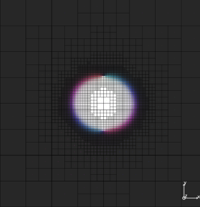
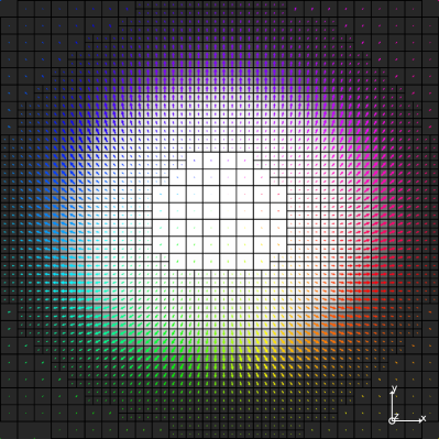
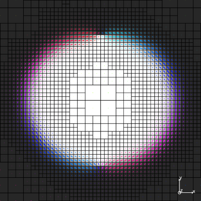
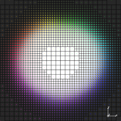
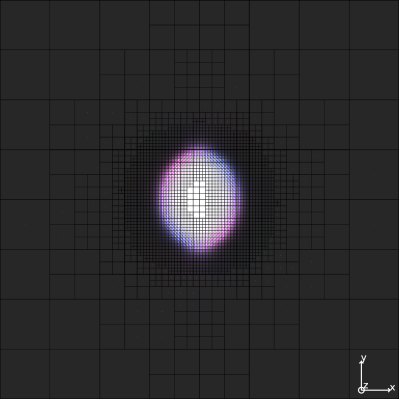
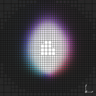
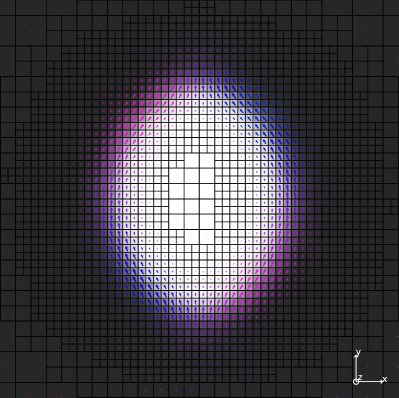
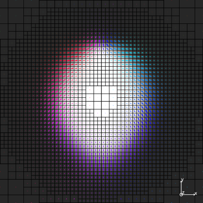
A further step can be made towards the comparison between simulated and experimental configurations by simulating Fresnel contrasts that would be obtained from the multiscale calculations. They are given in Fig. 11. Beside the result corresponding to Fig. 10, we report the results for a bubble without a BP. It can be seen that the position of the contrast and the shape of the bubble agree fairly well.
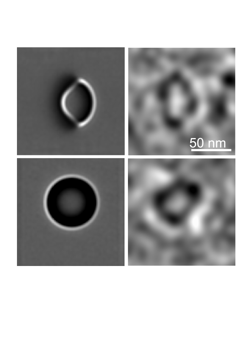
Despite the good agreement on the shape of bubbles, the transition from the BP-free to the BP configuration does not occur at the same thickness experimentally and in the simulations. Indeed, the configurations without BP are not stable in our simulations for a thickness of 37.6 nm (and even 20.7 nm), whereas according to the deformation of the bubbles observed in the samples, VBL contain a BP at this thickness. One reason for this discrepancy may be the presence of the soft layer on which the L10 layer is deposited. The exchange and demagnetizing contributions to the energy are modified due to the different closure of the magnetic flux. The thickness of the bottom Néel cap increasesMasseboeuf et al. (2008), which induces a dissymmetry in the system and could favor the configuration without BP.
IV Conclusion
Using Lorentz transmission electron microscopy on FePd samples and multiscale simulations, we have shown that it is possible to determine the magnetic structure of domain walls as thin as 8 nm. The presence of vertical Bloch lines in some bubbles has been demonstrated by microscopy. Bubbles containing two vertical Bloch lines exhibit a distortion of the classical circular shape. The simulation of entire bubbles has been possible thanks to the multiscale approach and has revealed that the deformation observed experimentally is a signature of the absence of Bloch points inside the vertical Bloch lines. For straight domain walls in FePd, we predict a larger buckling than previously reported for other materials.
References
- Seki et al. (2006) T. Seki, S. Mitani, K. Yakushiji, and K. Takanashi, Applied Physics Letters 88, 172504 (pages 3) (2006), URL http://link.aip.org/link/?APL/88/172504/1.
- Seki et al. (2008) T. Seki, S. Mitani, and K. Takanashi, Physical Review B (Condensed Matter and Materials Physics) 77, 214414 (pages 8) (2008), URL http://link.aps.org/abstract/PRB/v77/e214414.
- Hubert and Schäfer (1998) A. Hubert and R. Schäfer, Magnetic Domains – The Analysis of Magnetic Microstructures (Springer, 1998).
- Thiaville and Miltat (1990) A. Thiaville and J. Miltat, Journal of Applied Physics 68, 2883 (1990).
- Slonczewski (1974) J. C. Slonczewski, Journal of Applied Physics 45, 2705 (1974), URL http://link.aip.org/link/?JAP/45/2705/1.
- Hubert (1974) A. Hubert, AIP Conference Proceedings 18, 178 (1974), URL http://link.aip.org/link/?APC/18/178/1.
- Nakatani and Hayashi (1988) Y. Nakatani and N. Hayashi, Magnetics, IEEE Transactions on 24, 3039 (1988).
- Miltat et al. (1989) J. Miltat, A. Thiaville, and P. Trouilloud, Journal of Magnetism and Magnetic Materials 82, 297 (1989).
- Chapman (1984) J. Chapman, Journal of Physics D : Applied Physics 17, 623 (1984), lorentz.
- Aitchison et al. (2001) P. Aitchison, J. Chapman, V. Gehanno, I. Weir, M. Scheinfein, S. McVitie, and A. Marty, Journal of Magnetism and Magnetic Materials 223, 138 (2001), fePd.
- Masseboeuf et al. (2009) A. Masseboeuf, C. Gatel, J. C. Toussaint, A. Marty, and P. Bayle-Guillemaud, Ultramicroscopy under review (2009).
- Dooley and De Graef (1997) J. Dooley and M. De Graef, Micron 28, 371 (1997), dPC.
- Masseboeuf et al. (2008) A. Masseboeuf, C. Gatel, A. Marty, J. C. Toussaint, and P. Bayle-Guillemaud, in Journal of physics: conference series (Institute of Physics Publishing, 2008), vol. 126, p. 012055.
- Jourdan et al. (2008) T. Jourdan, A. Marty, and F. Lançon, Physical Review B 77, 224428 (2008).
- Thiaville et al. (2003) A. Thiaville, J. M. García, R. Dittrich, J. Miltat, and T. Schrefl, Physical Review B 67, 094410 (2003).
- Gehanno et al. (1997) V. Gehanno, A. Marty, B. Gilles, and Y. Samson, Physical Review B 55, 12552 (1997).
- Hubert (1976) A. Hubert, Journal of Magnetism and Magnetic Materials 2, 25 (1976).
- Thiaville et al. (1991) A. Thiaville, J. B. Youssef, Y. Nakatani, and J. Miltat, 35th annual conference on magnetism and magnetic materials 69, 6090 (1991).
- Thiele (1970) A. A. Thiele, Journal of Applied Physics 41, 1139 (1970), URL http://link.aip.org/link/?JAP/41/1139/1.