Ferromagnetic proximity effect in F-QDot-S devices
Abstract
Ferromagnetic proximity effect is studied in InAs nanowire (NW) based quantum dots (QDs) strongly coupled to a ferromagnetic (F) and a superconducting (S) lead. The influence of the F lead is detected through the splitting of the spin-1/2 Kondo resonance. We show that the F lead induces a local exchange field on the QD, which has varying amplitude and sign depending on the charge states. The interplay of the F and S correlations generates an exchange field related subgap feature.
Superconductor-ferromagnet (S/F) heterostructures have been investigated extensively in the past and they have potential impact on the field of spintronics and quantum computation. Due to the different spin ordering of textcolorreda s-wave superconductor and a ferromagnet, a large variety of interesting phenomena can be studied at a S/F interface: probing the spin polarization by Andreev reflection Soulen et al. (1998), -junction behaviour Kontos et al. (2001); Zareyan et al. (2001), ferromagnetically induced triplet superconductivity Keizer et al. (2006) or ferromagnetically assisted Cooper pair splitting Beckmann et al. (2004).
Here we focus on a novel S/F hybrid device where a quantum dot (QD) is incorporated between a S and a F lead. Recently, the modification of the Andreev reflection of such hybrid sytems has been calculated Feng et al. (2003); Cao et al. (2004). Also configurations, where a QD is strongly coupled to two F leads (F-QDot-F) attracted increasing theoretical Martinek et al. (2003); Choi et al. (2004); Cottet et al. (2004, 2006) and experimental Sahoo et al. (2005); Pasupathy et al. (2004); Hamaya et al. (2007); Hauptmann et al. (2008) attention. It has been verified Pasupathy et al. (2004); Hamaya et al. (2007); Hauptmann et al. (2008), that in this situation the spin- and energy levels of the QD can split by an exchange energy, due to the hybridization between the QD states and the F lead. This proximity ferromagnetism has the same effect on the QD as the presence of an external magnetic field, . Thus, the exchange splitting is often characterized by the so-called local magnetic exchange field () in the literature, where . As has been proposed by Martinek Martinek et al. (2005), can be gate dependent and even change sign. Hence, electric controlled reversal of the spin occupation of the QD can be achieved. This has very recently been shown in carbon nanotubes with two F contacts Hauptmann et al. (2008).
In this work, we show the influence of F and S correlations on the transport properties of F-QD-S devices. We
demonstrate that already a single F lead introduces a local exchange field which strongly varies for different QD
levels. Furthermore, it even can change its sign within the same charge state. On the other hand, the presence of the S
contact serves as a spectroscopic tool. Concentrating on the subgap transport, a novel mini-gap feature is observed,
which is related to .
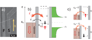
A typical device is shown in Fig. 1a. We use high-quality molecular beam-epitaxy grown InAs nanowires (NWs). NWs are dissolved in IPA and deposited on doped Si substrates with nm insulating SiO2. Afterwards, ohmic contacts at spacings of nm are fabricated. The F contacts consist of a Ni/Co/Pd trilayer (15 nm/80 nm/10 nm), whereas the S ones consist of a Ti/Al bilayer (10 nm/110 nm). Prior to metal evaporation, argon gun sputtering is used to remove the native oxide layer from the nanowires. In agreement with our previous measurements, QDs form between these contacts, which can be tuned by the voltage applied on the backgate, Csonka et al. (2008); Jespersen et al. (2006). Measurements are performed at a temperature of mK. A field is applied parallel to the easy axis of the F contact which is defined by shape anisotropy (see Fig. 1a). The field allows to switch the orientation of the F stripe and to control the size of the superconducting gap. To magnetize the F lead the external field is ramped to mT and then back to mT before measuring.
In Fig. 1b the energy diagram of our devices is shown schematically. The F lead induces an asymmetry of the tunnel coupling () of spin- and spin- electrons to the QD, described by the tunneling spin polarization . This asymmetry is caused by the difference of the spin- and spin- electron density of the F lead at the Fermi energy and by the tunneling matrix elements of these electrons. E.g. in Ni at two bands couple with opposite spin-imbalance and very different tunneling matrix elements to the QD Mazin (1999). By hybridization, the spin dependent tunnel coupling generates a spin imbalance on the QD, described as an exchange field. The S lead is represented by the BCS density of states (DOS) with its energy gap, .

In order to investigate the ferromagnetic proximity effect, the QD is operated in the strongly coupled regime, which allows the study of the cotunneling induced manybody spin-1/2 Kondo resonance Goldhaber-Gordon et al. (1998) at odd occupation number of the QD. Kondo resonances split into a doublet in a field according to the Zeeman energy , thus being also a sensitive tool to visualize . Probing the exchange splitting by the Kondo effect has been demonstrated in C60-molecules Pasupathy et al. (2004) and carbon nanotubes based QDs Hauptmann et al. (2008). InAs NW QDs have the advantage that the g-factor can be comparable to the bulk value of g15 Csonka et al. (2008), making them particularly sensitive for studying the level splitting created by . Much smaller external fields are needed to access the regime, where the exchange energy and the Zeeman splitting are comparable.
The ferromagnetic proximity effect and the therewith connected ground state transition on the QD can be described in a simple model. Using perturbative scaling analysis for a flatband bandstructure with spin dependent tunneling rates and including finite Stoner splitting in the leads an analytical formula for the energy splitting of the spin- and the spin- is found Martinek et al. (2005):
| (1) |
Here is as defined earlier, is the coupling to the F lead (), the charging energy of the QD and the level position of the QD, tunable by . is the Zeeman splitting due to an external magnetic field, is a Stoner splitting induced shift. Elaborated NRG calculations also support the result of Eq. 1 Martinek et al. (2005). Interestingly, based on Eq. 1, the spin ground state of the QD is different for close to than for close to , if or the Zeeman term are not too big. This change in the ground state of the QD can be explained by the charge fluctuations between the QD and the F lead (see Fig. 1c). Electrons with majority tunneling spin orientation dominate the charge fluctuations. Thus, when the QD occupation fluctuates between and (), the majority tunneling spin occupies the QD preferably. However, when the occupation fluctuates between 1 and 2 (), the remaining (non fluctuating) spin on the QD has the minority spin orientation of the tunneling electrons Martinek et al. (2005); Hauptmann et al. (2008). The transition between these opposite ground states is described by the sign change of the exchange field in Eq. 1. However, if is the dominant term, a roughly constant splitting of the Kondo resonance is expected within a charge state.

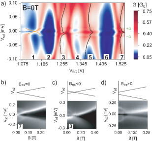
In Fig. 2a the differential conductance as a function of and source drain voltage , , of several charge states of a studied F-QD-S device is presented. Measurements were performed with standard lock-in technique with an ac excitation of eV. In accordance with the spin-1/2 Kondo effect, pronounced conductance is seen around ( V) in every odd charge state. However, in these states (labeled with numbers 1,3,5,7) the Kondo resonance shows different signatures due to correlations induced by the F lead. State 7 demonstrates a spin-1/2 Kondo situation with a single resonance line at V. As it is shown in Fig. 2b this zero bias Kondo resonance splits up linearly with . In contrast, state 3 exhibits clear signature of F correlations, i.e. the Kondo resonance has a finite and roughly constant splitting at mT (see black cross-section). Fig. 2c shows, that this splitting is compensated by mT and split again at higher fields. Thus has an opposite sign as the field. Another type of dependence of the Kondo ridge is presented in Fig. 2d (measured at V), where the zero field splitting of the resonance is further increased by an applied field. It means, that is parallel to for this state. The three markedly different field behaviors (Fig. 2b-d) demonstrate that strongly depends on the QD level. Even in a small backgate range the amplitude and the sign of varies. This observation highlights the particular importance of the coupling of the QD state to the F lead for the charge fluctuations induced local exchange field Martinek et al. (2005). Note, the different dependencies also prove that the observed effect can not solely be described by stray field, since the stray field cannot depend on .
The most interesting class among the different exchange field manifestations is the one of state 1 (see Fig. 2a). The Kondo resonance is also split for this state. However the size of the splitting strongly varies with . (The resonance lines are highlighted with dashed lines in Fig. 2a). Interestingly, the split Kondo resonance lines also cross the mV value inside the charge state. This dependence suggests that within this charge state first gets smaller as is increased. With further increasing it changes its sign and increases further in the opposite direction. This situation corresponds to the electrically controlled ground state transition on the QD described by Eq. 1 and Fig. 1c.

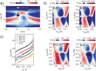
Since in situations like state 1 of Fig. 2a is strongly gate dependent, a measure for the exchange splitting at different gate voltages can be obtained by measuring the compensation field for which the Kondo peak is restored. Thus, if one measures at mV, at each signatures of high conductance are expected if due to the restored Kondo resonance. Such a plot is presented in Fig. 3a. The lower/upper ridge (see dashed lines) defines the resonance positions when the occupation of the QD level changes between /. The white arrow indicates the sweep direction of . The high conductance lines with finite slope show the evolution of the Kondo resonance (marked with a white line). At each field the gate position of the restored Kondo resonance defines the border between the spin- and the spin- ground states. At high external magnetic fields (i.e. T) the Zeeman term dominates (see Eq. 1). Therefore, considering that the g-factor of InAs is negative, the spin- is the ground state for all gate values in high field and the Kondo resonance coincides with the border at . As the field decreases the restored Kondo peak moves towards , opening backgate regions where spin- is the ground state. At mT the spin- state dominates, and spin- remains only in a small gate region around the preferable spin orientation. The gate voltage value as a function of , where the spin ground state change takes place, can be expressed with Eq. 1 using the condition of . The white line in Fig. 3a shows such a curve, giving a reasonable agreement with the measurement using the parameters of , mT and meV.
As the polarization of the F lead is switched to the opposite direction by a field larger than the coercive field of the contact, also changes its sign. This appears as a step in the measurement (see Fig. 3a) since the splitting turns from to . Due to the high g-factor of the InAs QD state, this is clearly seen in Fig. 3a at the position of the black arrow. Note, that in the vicinity of the border at mT, the ground state is spin-. At this border the preferable spin orientation on the QD is the majority tunneling spin orientation (see Fig. 1c). Martinek et al. (2005); Hauptmann et al. (2008) Since the F lead has been previously polarized into spin- state by a positive field, we can conclude, that the polarization of the F lead and the polarization of tunneling electrons are the same.
Eq. 1 describes the energy difference between the spin- and the spin- states as a function of . This is equivalent with the energy (), where the Kondo ridge appears. of state 1 is also measured in different magnetic fields. As it is seen in Fig. 3b, the position of the more pronounced split Kondo line moves to higher source drain voltage values as is increased. The , coordinates of this line is read out from the measurements, see e.g. the dotted line for T. Fig. 3c summarizes the measured position of the Kondo ridge by symbols at different fields. The theory described by Eq. 1 nicely fits the experiment (see lines) with the parameters used for the plot in Fig. 3a.

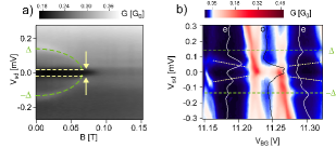
Since our device has a novel hybrid configuration, i.e. a QD connected to one F and one S lead, the interplay of S and F correlations can be studied. Up to this point, charge states with Kondo physics were investigated, where the Kondo resonance dominates the low energy behavior also for the S state. For such states the S lead induces conductance maxima at related to the singularities of the S DOS, which diminish with increasing B field. However, in several charge states of different devices, where spin-1/2 Kondo resonances are not present (neither in the S nor in the normal state), an interesting subgap feature appears. This is shown in Fig. 4a, where the measurement of such a state is presented. The conductance shows in a bias window of V significantly smaller values than in the rest of the superconducting gap (see horizontal dashed line). This mini-gap is clearly connected to superconductivity since it is suppressed above the critical field of the S lead. On the other hand the energy scale of the novel subgap feature coincides with the exchange energy observed in the split Kondo states (see e.g. Fig. 2d). It suggests that the subgap is also exchange field related. Further evidence for such an relation is shown in the measurement at mT on an other device (see Fig. 4b). The middle charge state with odd electron filling () shows a slightly split Kondo resonance, while the two even states () demonstrate the new subgap feature. As it is shown by the dotted lines, the mini-gap lines of the even charge states merge into the split Kondo resonance at the border between the even and the odd states. Thus, superconductivity induced transport processes in charge states with an even electron number are presented, which seem to be correlated with the exchange splitting.
Concluding, our measurements demonstrate that ferromagnetic proximity effect is indeed present in InAs NW based F-QD-S devices. A single F lead induces a local exchange field on the QD, which is strongly level dependent: it even changes sign for a single charge state. Demonstration of controlling the spin ground state of the QD by electric means makes the F-InAs QD-S system a promising building block for spin correlation studies, if implemented into a Cooper pair splitter device Hofstetter et al. (2009); Herrmann et al. (2010).
We thank L. Borda, V. Koerting for fruitful discussions and C.B. Soerensen, III-V Nanolab, Niels Bohr Institute for MBE growth. This work has been supported by the Swiss NSF, the NCCR on Nanoscale Science, the Danish Natural Science Research Council, the OTKA-Norwegian Financial Mechanism NNF 78842, OTKA 72916 and the EU M.C. 41139 projects. S. C. is a grantee of the Bolyai Janos Scholarship.
References
- Soulen et al. (1998) R. J. Soulen, J. M. Byers, M. S. Osofsky, B. Nadgorny, T. Ambrose, S. F. Cheng, P. R. Broussard, C. T. Tanaka, J. Nowak, J. S. Moodera, A. Barry, J. M. D. Coey, Science 282, 85 (1998).
- Kontos et al. (2001) T. Kontos, M. Aprili, J. Lesueur, and X. Grison, Phys. Rev. Lett. 86, 304 (2001).
- Zareyan et al. (2001) M. Zareyan, W. Belzig, and Y. V. Nazarov, Phys.Rev. Lett. 86, 308 (2001).
- Keizer et al. (2006) R. S. Keizer, S. T. B. Goennenwein, T. M. Klapwijk, G. Miao, G. Xiao, and A. Gupta, Nature 439, 825 (2006).
- Beckmann et al. (2004) D. Beckmann, H. B.Weber, and H. v. Lohneysen, Phys. Rev. Lett. 93, 197003 (2004).
- Feng et al. (2003) J. F. Feng, and S. J. Xiong, Phys. Rev. B 67, 045316 (2003).
- Cao et al. (2004) X. F. Cao, Y. Shi, X. Song, S. Zhou, and H. Chen, Phys. Rev. B 70, 235341 (2004).
- Martinek et al. (2003) J. Martinek, Y. Utsumi, H. Imamura, J. Barnas, S. Maekawa, J. Konig, and G. Schon, Phys. Rev. Lett. 91, 127203 (2003).
- Choi et al. (2004) M. S. Choi, D. Sanchez, and R. Lopez, Phys. Rev. Lett. 92, 056601 (2004).
- Cottet et al. (2004) A. Cottet, T. Kontos, W. Belzig, C. Schönenberger and C. Bruder, Europhys. Lett. 74, 320-326 (2006).
- Cottet et al. (2006) A. Cottet, and M. S. Choi, Phys. Rev. B 74, 235316 (2006).
- Sahoo et al. (2005) S. Sahoo, T. Kontos, J. Furer, C. Hoffmann, M. Gräber, A. Cottet, and C. Schönenberger, Nature Physics 1, 99 (2005).
- Pasupathy et al. (2004) A. N. Pasupathy, R. C. Bialczak, J. Martinek, J. E. Grose, L. A. K. Donev, P. L. McEuen, and D. C. Ralph, Science 306, 86 (2004).
- Hamaya et al. (2007) K. Hamaya, M. Kitabatake, K. Shibata, M. Jung, M. Kawamura, K. Hirakawa, T. Machida, T. Taniyamae, S. Ishida, and Y. Arakawab, Appl. Phys. Lett. 91, 232105 (2007).
- Hauptmann et al. (2008) J. R. Hauptmann, J. Paaske, and P. E. Lindelof, Nature Physics 4, 373 (2008).
- Martinek et al. (2005) J. Martinek, M. Sindel, L. Borda, J. Barnas, R. Bulla, J. Konig, G. Schoen, S. Maekawa, and J. von Delft, Phys. Rev. B 72, 121302(R) (2005).
- Csonka et al. (2008) S. Csonka, L. Hofstetter, F. Freitag, S. Oberholzer, T. S. Jespersen, M. Aagesen, J. Nygår, and C. Schönenberger, Nano Lett. 8, 3932 (2008).
- Jespersen et al. (2006) T. S. Jespersen, M. Aagesen, C. Sorensen, P. E. Lindelof, and J. Nygard, Phys. Rev. B 74, 233304 (2006).
- Mazin (1999) I. I. Mazin, Phys. Rev. Lett. 83, 1427-1430 (1999).
- Goldhaber-Gordon et al. (1998) D. Goldhaber-Gordon, H. Shtrikman, D. Mahalu, D. Abusch-Magder, U. Meirav, and M. A. Kastner, Nature 391, 156 (1998).
- Hofstetter et al. (2009) L. Hofstetter, S. Csonka, J. Nygård, and C. Schönenberger, Nature 461, 960-963 (2009).
- Herrmann et al. (2010) L. G. Herrmann, F. Portier, P. Roche, A. L. Yeyati, T. Kontos, and C. Strunk, Phys. Rev. Lett. 104, 026801 (2010).