μ
Nanowire atomchip traps for sub-micron atom-surface distances
Abstract
We present an analysis of magnetic traps for ultracold atoms based on current-carrying wires with sub-micron dimensions. We analyze the physical limitations of these conducting wires, as well as how such miniaturized magnetic traps are affected by the nearby surface due to tunneling to the surface, surface thermal noise, electron scattering within the wire, and the Casimir-Polder force. We show that wires with cross sections as small as a few tens of nanometers should enable robust operating conditions for coherent atom optics (e.g., tunneling barriers for interferometry). In particular, trap sizes on the order of the deBroglie wavelength become accessible, based solely on static magnetic fields, thereby bringing the atomchip a step closer to fulfilling its promise of a compact device for complex and accurate quantum optics with ultracold atoms.
pacs:
42.50.Ct, 37.10.Gh, 12.20.-mI Introduction
Trapping atoms in magnetic traps using atomchips Folman et al. (2002); Reichel (2002); Fortágh and Zimmermann (2007) allows ultracold atoms or a Bose-Einstein Condensate (BEC) to be manipulated and interrogated very close to the atomchip surface. Though outstanding achievements have already been made for atom-surface distances of , e.g., spatial interference Schumm et al. (2005); Jo et al. (2007) as well as hyperfine state interferometry Treutlein et al. (2004), it remains of paramount importance to understand what ultimately limits the atom-surface distance. Further decreasing the atom-surface distance should increase trap gradients sufficiently to construct tunneling barriers with widths on the order of the atomic deBroglie wavelength, enabling e.g., atomchip interferometry based solely on static magnetic fields. Such high trap gradients may also allow more robust atom-light interactions such as probing without heating in the Lamb-Dicke regime. Furthermore, sub-micron distances are also important for technological advantages such as low power consumption and high-density arrays of traps.
At small atom-surface distances, interactions with the nearby surface become important. For example, spatial and temporal magnetic field fluctuations, due to electron scattering and Johnson noise respectively, limit the minimum atom-surface distance, as they cause potential corrugations, spin flips, and decoherence. There have been several experiments utilizing cold atoms to study these interactions Fortágh et al. (2002); Jones et al. (2003); Estève et al. (2004); Wildermuth et al. (2005); Aigner et al. (2008); Emmert et al. (2009), and many suggestions on how to overcome their damaging effects Dikovsky et al. (2005); Trebbia et al. (2007); Fermani et al. (2007); Japha et al. (2008); David et al. (2008); Petrov et al. (2009).
Also becoming prominent for small atom-surface distances is the Casimir-Polder (CP) force Sukenik et al. (1993); normally attractive, it reduces the magnetic barrier and allows atoms to tunnel to the surface, as already observed Lin et al. (2004); Obrecht et al. (2007). At very small distances the atoms may also serve as a sensitive probe for surface phenomena; for example, plasmons are expected to affect the atomic external and internal degrees of freedom and may also become observable Intravaia et al. (2007).
From the above it is evident that achieving small atom-surface distances would not only be advantageous for atom optics, but would also contribute to the fundamental study of surface phenomena. Finally, let us note that there are numerous ideas for bringing atoms closer to the surface Ovchinnikov et al. (1991); Schmiedmayer (1998); Shevchenko et al. (2004); Rosenblit et al. (2006); Ricci et al. (2007); Bender et al. (2009); Gillen et al. (2009), all of which are, however, based on interactions with fields other than static magnetic fields, the latter being the focus of this work. We consider wires operating at room temperature, fabricated using standard methods, in contrast to suspended molecular conductors Peano et al. (2005); Fermani et al. (2007) and superconductors, that reduce the Casimir-Polder force and noise originating in the surface Dikovsky et al. (2009); Emmert et al. (2009); Roux et al. (2008); Mukai et al. (2007); Cano et al. (2008); Emmert et al. (2008) respectively.
The paper is organized as follows: in Sec. II we show qualitatively that creating static potential barriers on the scale of atomic deBroglie wavelengths, and therefore suitable for controlling tunneling, require micron or sub-micron atom-surface distances. In Sec. III we present the physical properties of gold nanowires, including a theoretical analysis of their resistivity. In Sec. IV we analyze the potentials expected from such nanowires, including the Casimir-Polder force and potential corrugation effects. We show that improved fabrication methods can overcome earlier limitations due to trapping potential roughness Estève et al. (2004), which at sufficiently small separations would otherwise cause the trapped atomic cloud to break into smaller clouds (fragmentation). In Sec. V, we estimate trap lifetimes limited by atom losses due to noise-induced spin flips, Majorana spin flips, and tunneling. In particular, we show how the spin-flip rate induced by Johnson noise is reduced naturally by using very small amounts of material in the nanowires. We also consider the issue of decoherence. In Sec. VI we discuss a simple trap configuration based on a Z-shaped gold wire. We show that such a nanowire structure can generate static magnetic potentials, smooth enough for trapping a BEC at sub-micron atom surface separations. Finally, in Sec. VII we briefly discuss nanowire traps fabricated by more exotic materials.
II Static magnetic potentials for atom interferometry
Two technical characteristics of potentials that are required in order to study atom interferometry can be described in the following way: first, the potential barrier between adjacent wells should be sufficiently low or narrow so that the tunneling rate is comparable to, or faster than, typical experimental or dephasing time scales; and second, that this tunneling rate can be controlled with experimentally accessible currents and fields.
Largely because of the weak dependence of the magnetic potential on the atom-wire distance, these tunneling conditions require very short distances. To quantify this, we construct a simple waveguide potential using a single atomchip wire (in the x-direction) and an external bias field; current through a second atomchip wire (in the y-direction) is added to generate a simple potential barrier in a right-angle “X” wire configuration Hänsel et al. (2001). This configuration incidentally is exactly opposite to the “dimple” configuration recently used for compressing atomchip traps Horikoshi and Nakagawa (2006); Anderson (2009).
The magnetic potential in the direction, generated by the crossing wire, is given by:
| (1) |
where is the atomic magnetic dipole moment along the direction of the Ioffe field , is the current in the crossing wire, is the permeability of free space, and is the distance of the atom from the atomchip surface. A one-dimensional single-particle tunneling probability through the barrier can then be calculated in the WKB approximation as
| (2) |
where is the kinetic energy of the atom and . Assuming a kinetic energy of for a atom (corresponding to a free-particle deBroglie wavelength of ) in the state, we may then easily calculate the change required in the current that causes a given proportional change in the tunneling probability, as a function of the atom-surface distance . The results of this calculation are shown in Fig. 1 for changing the tunneling probability from 0.001 to some higher probability. The calculation suggests that control over the tunneling probability requires a distance on the order of for experimentally reasonable values of current control. In the simple model of Eq. (1), this corresponds to a barrier half-width of , comparable to experiments that have observed interference between adjacent wells with the addition of non-static fields Schumm et al. (2005); Jo et al. (2007). Thus, the desired static magnetic potentials can be generated only if atoms can be brought down to micron or sub-micron distances above the wires on the atomchip surface, at which point the tunneling rate can be tuned over an experimentally useful dynamic range by adjusting the current in the crossing wire. One may then envisage interferometric devices such as the ones we have proposed in Refs. Rohrlich et al. (2006) and Japha et al. (2007).
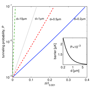
It is well known that, to avoid finite size effects which degrade the trap gradient, the wire size should be on the same scale as the atom-surface distance, i.e., for the above noted heights of (see Fig. 1) one requires a micron-scale wire. As will be shown in the following, it is advantageous to utilize even smaller wire dimensions, namely nanowires. This will enable improving operational parameters at the above heights, or decreasing the atom-surface distance even further without hindering effects.
III Physical properties of thin wires
III.1 Wire fabrication and characterization
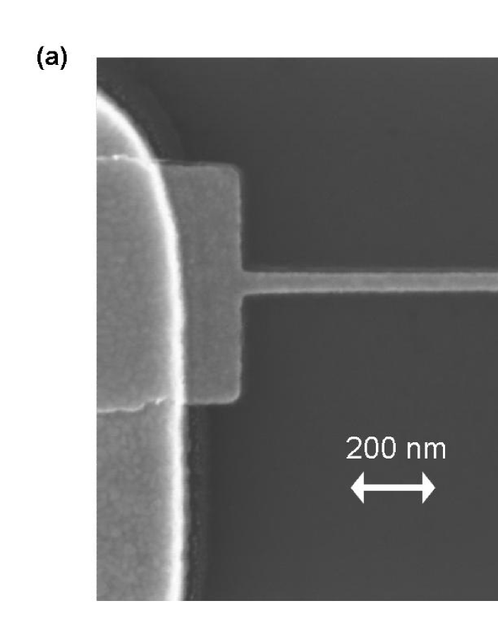
In order to study the possibility of trapping atoms using nanowires, we first discuss the fabrication feasibility. An example of one such (short) wire, thick and wide, is shown in Fig. 2(a). This wire was prepared by us in a relatively simple two-step process involving optical lithography (for external connection) followed by electron-beam lithography (for the nanowires). A Si substrate with a well-defined oxide layer of thickness and a thin -thick Ti adhesion layer is spin-coated with image reversal photoresist, which is then exposed to ultraviolet light through a mask. After developing, a -thick Ti seed layer, followed by a -thick Au layer, is then evaporated onto the sample and the undeveloped areas lifted off, leaving large areas for connection to external testing equipment. The sample is then spin-coated with a layer of PMMA, and the nanowire plus several of the interconnects are patterned by electron-beam lithography. After developing, gold is evaporated onto the sample with the desired thickness and the fabrication is completed with a final lift-off process. This fabrication process can easily be integrated with any atomchip design.
Using SEM images of the fabricated wires, we measured the edge roughness of the resulting wires, as shown in Fig. 2(a). The spectrum of this edge roughness can be characterized as frequency-independent (“white noise”) with a measured root-mean-square deviation of for wavelengths of .
III.2 Wire resistance calculations
The resistivity of a nanowire increases beyond the bulk resistivity as the cross-section dimensions become comparable to the mean free path of an electron ( for gold at room temperature Ashcroft and Mermin (1976)). In such a small wire the resistivity may increase significantly Durkan and Welland (2000a); Steinhögl et al. (2002). To estimate the change of resistivity in a nanowire, we follow the theoretical model of Fuchs and Sondheimer Fuchs (1938); Sondheimer (1952), which was extended by Chambers Chambers (1950). This model is supported experimentally for gold nanowires Durkan and Welland (2000a). For wire dimensions on the order of the grain size, a supplementary model by Mayadas and Shatzkes Mayadas and Shatzkes (1970) is needed in order to account for scattering at grain boundaries. For the simple fabrication process we have described, the measured grain size is about , so for wire dimensions above this size we can attribute the increase in nanowire resistivity solely to scattering at the walls as in the Fuchs-Sondheimer model Durkan and Welland (2000b).
For atomchip experiments, we are interested in the current density in the wire and not only the wire resistance. Therefore we give the current density in a wire (along ) of width (along ) and thickness (along ) as
| (3) |
where is the current density expected in the absence of surface scattering, and 111Note the changes we have made to Eq. (1) in Durkan and Welland (2000a) and to Eq. (2) in Steinhögl et al. (2002).
| (4) |
corresponds to scattering at the boundary, corresponds to scattering at the boundary, and and , corresponding to scattering at the and boundaries respectively, are obtained by replacing by and by . The resulting resistivity is given by , where is the bulk resistivity. It follows that the current density at the metallic layer near the boundary drops to its value far from the boundary. To account for surface scattering, one assumes a fraction () of specular reflection events at the boundaries; then the value of the resistivity is given by a series expansion
| (5) |
where is the resistivity calculated for a wire with totally diffusive scattering at the boundaries () and a mean free path . Measurements of resistivity of thin gold wires are well reproduced by a theory assuming Durkan and Welland (2000a); Steinhögl et al. (2002). Figure 2(b) shows that the calculated resistivities for wires with square cross-sections increase by up to about 50% for cross-sections down to .
III.3 Current limitations
Forming magnetic traps deep enough to hold ultracold atoms near the surface of an atomchip requires sufficiently large currents in the microfabricated wires to ensure that the trapping potential overcomes the gravitational force, the Casimir-Polder attraction to the chip surface, and the kinetic and repulsive energy of the atoms. However, if the current is too high, the wire overheats and may eventually break down Groth et al. (2004). The wire temperature is determined by the balance between ohmic heating (whose power dissipation per unit area is ) and the rate of heat conduction to the wafer per unit area , where is the thermal contact resistance of the wire-wafer interface and is the difference between the temperature of the wire and the temperature of the wafer (typically room temperature). The heat capacity of nanowires is so small that the wire reaches its maximum temperature very rapidly; approximating the temperature dependence of the resistivity as that of bulk gold, whose linear coefficient is , we obtain the current density required to heat a given wire by a temperature as Groth et al. (2004)
| (6) |
thus showing that thin wires allow higher current densities. On the other hand, if the wire cross-section is on the order of the mean free path of the electrons, the rise in the resistivity due to surface scattering [Fig. 2(b)] may limit this advantage. In Fig. 2(c) we present the calculated maximum current density for different wire cross-sections using an estimated value for from Ref. Groth et al. (2004), and assuming that we limit the rise in resistivity (due to heating) to 50%, which we consider to be within safe operating limits for thin atomchip wires Groth et al. (2004). This limitation in the resistivity change corresponds to heating by .
IV Atomic trapping potential
In this section we describe two prominent effects influencing the static potential at sub-micron atom-surface distances generated by nano-scale wires, namely corrugations due to electron scattering, and tunneling to the surface or the nanowire, through the magnetic potential, due to the Casimir-Polder force.
IV.1 Potential Corrugations
One of the limiting factors when trapping or guiding atoms in a magnetic potential generated from a current carrying wire is the static potential corrugation due to current deviations Aigner et al. (2008); Japha et al. (2008). Such current irregularities are produced by wire imperfections, namely, geometrical properties (wire edge roughness and surface roughness), and internal bulk inhomogeneities. Since atomchip traps are formed by canceling the magnetic field generated by the current density at a specific distance from the wire , the minimum of the trapping potential lies along the wire direction . Variations in this potential are then directly related to changes in the direction of the magnetic field generated by the wire imperfections.
In previous work Aigner et al. (2008); Japha et al. (2008), we concluded that internal bulk inhomogeneities play a minor role in thin wires (). For wide wires, surface roughness dominates the potential corrugation, but as we show below, edge roughness dominates for narrow wires. Consequently, in this work we need to consider only current deviations due to edge roughness since all of the nanowires considered are thinner and narrower than .
Let us consider a fabricated metal wire carrying a total current . It extends along the direction and has a width along and thickness along . The boundaries of the wire are located at and . The corrugations of the wire boundaries and can be expanded as
| (7) |
A linear theory for small corrugations predicts that the effect of each spectral component of the corrugation is responsible for a corrugation of the magnetic field near the atomic trap center with a similar wavelength along the direction. However, the effect of components with wavelength much shorter than the distance between the wire and the atomic trap (on the order of hundreds of nanometers or more) drops exponentially as so that here we will only be interested in corrugations whose wavelengths are a few hundred nanometers or longer. We may then neglect the effect of spectral components on the order of the wire width or thickness and consider only corrugation terms with and , i.e., we may assume that and depend only on .
Corrugations of the magnetic field along the main trapping axis above the center of a wire with geometrical perturbations are given by the Biot-Savart law as
| (8) |
where are the transverse current fluctuations in the wire. At the point exactly above the center of a nominally symmetric wire, it follows that only the symmetric components of [] and the anti-symmetric components of [] contribute to the magnetic field. The fabrication process typically provides wires whose edge corrugations are much larger than their top or bottom surface corrugations, so that the symmetric part of is the major contribution to the magnetic field fluctuations.
Ohmic theory, which is adequate when the width and thickness of the wire are much larger than the electron mean free path and whose use we justify below, predicts that for wavelengths longer than the wire width or thickness the symmetric -current fluctuations in the wire have the form
| (9) |
such that in the limit where , , where is the position of the actual center of the wire at a given point . Substituting this limit into Eq. (8) while assuming small deviations of the wire edges from their nominal position, and assuming that , i.e., the width of the wire is much smaller than the distance of the atom to the wire, we obtain the following expression for the magnetic field corrugations above the wire
| (10) |
where is the total current in the wire and is the modified Bessel function, which may be approximated by . Our model for the fluctuation spectrum assumes that , where is the edge fluctuation at some wavevector and then can be obtained by summing this spectrum over all . Typically, is a number between 0 (“white-noise spectrum”) and 1 (“1/f spectrum”), while is a random phase. It follows that the root-mean-square value of the field fluctuations is given by
| (11) |
If we assume that the distance is much shorter than the length of the measured wire, we obtain
| (12) |
where is the regular magnetic field at the direction. Here has units of (length)1/2-α and is given by
| (13) |
where the sum is over values taking integer multiples of up to a cutoff . Typical values of this sum for and are and respectively, when .
The same result should be obtained if we consider diffusive surface scattering. As we have seen in Sec. III.2, in nano-sized wires, the conductivity near the boundary is reduced by diffusive surface scattering (with a typical exponential decay length from the wire edge). This means that diffusive scattering is limited to a region of dimension smaller than . At the same time, the corrugation wavelengths relevant at the atom position, e.g., similar to or larger than the atom-surface distance, induce current density directional daviations away from the edge with an exponential decay length of . As most of the current will follow the corrugations of the boundary even in the case of surface diffusive scattering, such that the resulting -current fluctuations will again generate transverse components of the current proportional to the derivative . We thus use the ohmic theory whose general form was developed in Ref. Japha et al. (2008) to calculate the magnetic field corrugations above the wire.
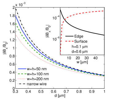
In Fig. 3 we present calculated directional variations of the magnetic field , generated by the trapping wire, as a function of the height for several wire cross-sections. The edge roughness amplitude is measured from our fabricated wires and was found to be frequency-independent [ in Eq. (12)] with a measured root-mean-square deviation of between 222We note that in the case of edge roughness with power spectrum (), the directional variations of the magnetic field will be an order of magnitude higher ( compared to at ), and will lead to significantly larger density perturbations.. In accordance with Eq. (12), we see that, for a given edge roughness , smaller wires produce only slightly larger magnetic corrugations. The effect of such magnetic corrugations on the atomic density will be discussed in Sec. VI. We also see that the influence of the surface roughness is negligible for the narrow wires discussed in this work due to the suppression of long wavelengths in the magnetic corrugations Japha et al. (2008).
IV.2 Engineering longitudinal potential variations by nanowire shaping
Shaping the nanowire edges may be used for creating potential variations desired for manipulating atoms near the atomchip surface. Having characterized the dependence of magnetic field variations on wire edge imperfections, we may now discuss quantitatively the deliberate “tailoring” of magnetic trapping potentials by engineering wire edge profiles. For the purposes of this study, as noted in the Introduction, we are particularly interested in potentials with sufficient variation so that tunneling barriers can be controlled. This is the main advantage of trapping atoms close to the trapping wire. Supplementing the motivation for a small atom-surface distance presented in Sec. II, we now wish to determine the highest “potential resolution”, i.e., the smallest distinguishable distance between adjacent wells separated by static tunneling barriers, as a function of .
As a test case for quantifying this potential resolution, we consider a configuration in which a thin wire is curved with a certain periodicity that corresponds to a wave-vector . If the amplitude of this curvature is small with respect to the wavelength, then the foregoing discussion implies that the magnetic field above the wire is given by a single component in Eq. (10), and then , where .
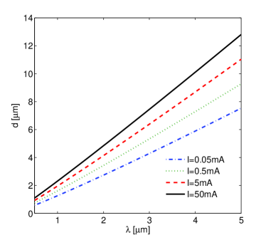
At the minima of such a periodic potential, the longitudinal frequency is , where is the atomic mass. In order to engineer potential barriers between adjacent minima higher by a factor of say, than the single-atom ground state energy, we require , or . In Fig. 4 we show the maximum atom-surface distance for which a longitudinal barrier with can be obtained. These curves show that the maximum atom-surface distance still allowing tunneling control is on the order of the potential periodicity . Designing the edges of a wire as the sum of different modulations therefore allows engineering of any periodic potential up to a resolution determined by the atom-surface distance. Consequently, as also seen in Sec. II, atom-surface distances of (or sub-micron distances in some cases) will be required to fully exploit the potential of an atomchip based on static magnetic fields.
IV.3 Attractive Casimir-Polder potential
The Casimir-Polder potential between a polarizable atom and dielectric or conducting objects Casimir and Polder (1948) is one of the fundamental outcomes of zero-point vacuum fluctuations. It emerges from the fact that a dielectric or conducting object modifies the modes of the electromagnetic (EM) field in its vicinity, modes which interact with the atomic polarization. In our case, an attractive Casimir-Polder potential arises from the conducting gold nanowire and from the Si wafer coated with a -thick SiO2 layer (used to prevent electrical shorts). The Casimir-Polder potential reduces the potential barrier for tunneling to the surface, thereby limiting the possibility of trapping atoms near the surface 333Note that numerous ideas on how to alter the Casimir-Polder force exist Intravaia et al. (2007); Leonhardt and Philbin (2007); Munday et al. (2009); Yannopapas and Vitanov (2009), and may, if proven successful, enable decreasing the atom-surface distance even further..
The EM modes of the combined surface+wire system are not analytically solvable and we will therefore carry out a separate examination of the Casimir-Polder potential emerging from the Si+SiO2 planar wafer, as discussed in earlier work Petrov et al. (2009), and from a simplified model that takes the wire as a perfectly conducting circular cylinder of a certain diameter. We then take the sum of the two contributions as an estimate for the combined potential as a sort of pairwise additive approximation, PAA. Based on our earlier experience from the planar two-layer system, we anticipate that this approach should at least give the right order of magnitude for the accurate Casimir-Polder potential.
In general, the Casimir-Polder potential may be written in the form
| (14) |
where is the frequency-dependent atomic polarizability and is the trace over the Green’s tensor of the electromagnetic field at the same point , with being the Green’s tensor in empty space, responsible for a space-independent Lamb shift. For distances from the dielectric or conducting object much larger than , where is the wavelength corresponding to the lowest optical transition frequency, the Casimir-Polder potential generated by a planar structure made from a layer of thickness with a dielectric constant atop an infinitely thick dielectric layer of dielectric constant has the form (see Appendix and Ref. Petrov et al. (2009))
| (15) |
where is the static atomic polarizability. The dimensionless function takes the single-layer limiting value with when , and with when , where is on the order of unity Yan et al. (1997). is obtained in the vicinity of a perfectly conducting thick layer. In our case is the ground state static polarizability of the atom Antezza et al. (2005), for the SiO2 layer, and for the Si wafer.
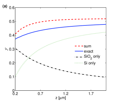
As stated above, we wish to compare contributions to the Casimir-Polder potential from the three different components comprising the surface: the Si chip, the SiO2 layer of thickness , and the gold nanowire of thickness . For this comparison to be meaningful, we require a common reference for the distance variable , which we define as the distance from the top of the SiO2 surface. Then the distance from the Si chip is and the distance from the top of the gold nanowire is . To factor out the strong dependence, we plot the quantity in Fig. 5(a) for the Si+SiO2 bilayer. This is compared to a sum of two models (shown separately in the figure): one where the half space for is full of Si while the other half is empty; and another in which only a -thick SiO2 layer exists, with empty space for . The figure shows that simply summing the two potentials over-estimates the exact result by 8-15% over the relevant range, but it gives the right order of magnitude.
Next we consider the Casimir-Polder potential for an atom at a distance from the center of a cylindrical conducting wire of radius where we set . It appears that the main contribution to the integral in Eq. (14) comes from frequencies on the order of . In our case, where , the skin depth for a gold wire with resistivity is , which is much smaller than the width or thickness of the nanowires considered. We can therefore use a model where the wire is perfectly conducting (impenetrable for EM waves), such that the EM Green’s tensor is much simpler than in the general case. The Casimir-Polder potential is then given by
| (16) |
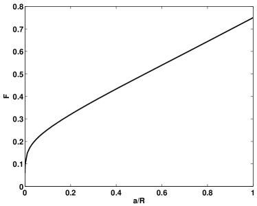
For the function is nearly linear, , tending to as , where the surface of the cylinder is similar to a planar conducting surface. In the opposite limit the function drops to zero as (see Appendix).
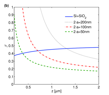
Figure 5(b) again shows the factor for the Casimir-Polder potential from the planar (i.e., Si+SiO2) surface in comparison to for cylindrical wires of different diameters . It is evident that the contribution of the wire is dominant when the distance from the wire is less than 5-7 times the diameter of the wire. For larger distances the contribution of the wire falls to half or less than the contribution of the surface. Given our experience with the bilayer system Petrov et al. (2009), we expect the exact calculation of the wire+surface to deviate by the same order as we observe for the bilayer, i.e., less than 20%. This degree of inaccuracy may also follow from the fact that the wires do not have circular cross-sections but square or rectangular ones. Therefore we believe that taking the sum of the two models can be expected to give at least an order of magnitude estimation of the Casimir-Polder potential.
V Atom loss
In this section we analyze the lifetime for atoms in the nanowire trap. This lifetime includes the spin-flip rate due to thermally induced noise, the Majorana spin-flip rate, and the tunneling rate to the surface. Finally, we estimate the decoherence rate due to the thermally induced noise in the room temperature surface.
V.1 Spin flip due to thermal noise
The magnetic thermal noise (Johnson noise) arising from conducting materials on the atomchip is coupled to the trapped atoms via their magnetic moment . As a consequence, spin flips, heating and decoherence become dominant close to a conductor even without applied currents. Here we calculate the trap loss rate due to spin flips. We assume that the spectrum of magnetic noise from the conductor is roughly constant for frequencies in the MHz region, the latter being able to drive magnetic transitions between Zeeman sub-levels in the same hyperfine level. In this case the magnetic moment is , where is the Bohr magneton, is the Landé factor for the hyperfine level and is the hyperfine spin operator. Using the theory developed by Henkel, the thermal spin-flip rate from an initial trapped Zeeman state to a final untrapped state can then be written as Henkel et al. (1999); David et al. (2008):
| (17) |
where we sum the contribution of all components of the noise perpendicular to the atomic magnetic moment. Here the function is the correlation function of the magnetic field noise, which is given by
| (18) |
with being a geometrical factor which also averages over if the resistivity changes in space:
| (19) |
The sum up the contribution of local fluctuations arising from each point in the conductor’s volume. We calculate Eq. (17) within the quasi-static approximation David et al. (2008); Henkel and Pötting (2001), which is valid when the atom-conductor distance is smaller than the skin depth ( is the Larmor frequency). This condition is easily met here since the skin depths of metals in the MHz region is typically tens of (e.g., gold has a skin depth of ).
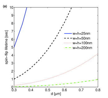
In Fig. 6(a) we present estimated lifetimes for trapped atoms due to thermal noise-induced spin flips. The wire size greatly affects the lifetime, mostly because smaller wires place much less conducting material near the atoms, and also because of their higher resistivity. For a wire, we estimate that the lifetime of a cloud trapped from the wire surface is , so we do not expect thermal noise-induced spin flips to be a dominant loss mechanism in typical experiments.
V.2 Majorana spin flips
Cold atoms in a low-field seeking state that are trapped near a vanishing magnetic field can undergo a spin-flip transition to a high-field seeking state that is untrapped (Majorana spin flips). Applying a small offset (Ioffe-Pritchard) field will generate a non vanishing field at the trap center, hence reducing the spin-flip transition rate as given by the approximate formula Sukumar and Brink (1997):
| (20) |
where is the trap radial frequency. Equation (20) is valid when the Larmor frequency , requiring that for typical radial frequencies. In the following sections, we choose a Ioffe-Pritchard field that simultaneously satisfies this condition and yields a Majorana spin-flip lifetime of .
V.3 Tunneling to the chip surface
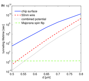
As a result of the Casimir-Polder potential, the magnetic barrier between the surface and the atoms is lowered, and atoms can tunnel through the barrier to the atomchip surface or wire. Calculated tunneling lifetimes are presented in Fig. 6(b), where we use a weighted average of the tunneling rate over all points in the plane. For each point we use the WKB approximation for tunneling through a one-dimensional potential barrier along the direction Petrov et al. (2009):
| (21) |
where is the chemical potential and the integration over is between the classical turning points and defined by . The weighted tunneling probability appearing in the integrand is given at any point by , where is the particle density and the transverse frequency is the inverse of the average round-trip time for a particle moving between the turning points []. These quantities are all calculated by solving the Gross-Pitaevskii equation for 1000 atoms of . In a typical trap generated by a Z-shaped wire (e.g., see Sec. VI), most of the tunneling occurs either at the center of the trap (where the atoms are closest to the wire) or at the trap ends (where the potential curves down towards the surface). Because of the much higher atom density directly above the wire, the lifetime is governed mostly by tunneling to the wire rather than to the surface, as discussed further in Sec. VI.
V.4 Spatial decoherence
As we have noted above, fluctuations of the magnetic field perpendicular to the quantization axis of the atom may cause transitions of the atom between Zeeman states defined along this axis. Conversely, fluctuations of the magnetic field along the quantization axis cause spatially dependent energy fluctuations, which may be viewed as potential fluctuations for the atom. These potential fluctuations imply that the phase of the atomic wavefunction at two locations and will also fluctuate, giving rise to dephasing. Again, we find that the mean square of the phase difference after a time is given by
| (22) |
where is the magnetic field component along the quantization axis. For a time scale much longer than the inverse of the magnetic noise bandwidth, we may take the random-walk limit , where is the magnetic field correlation tensor of Eq. (18) along the coordinate of the quantization axis. It then follows that the square of the phase difference grows linearly with time. This implies, in accordance with the theory developed by Henkel Henkel et al. (2003), that the coherence, which may be defined as , drops exponentially with the standard deviation of the difference, i.e., , with
| (23) |
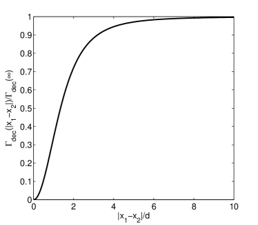
Figure 7 shows the decoherence rate of a split atomic wavefunction at two points located at an equal distance above an infinitely long and thin wire, as a function of the longitudinal separation between the points. Similar results are obtained when the two points are located above two separate parallel wires creating a local potential minimum above each of them, as a function of the separation between the two wires (and consequently between the two points). When the distance between and is much larger than the distance to the wire, the correlation term becomes negligibly small and the decoherence rate depends only on the distance of the two points from the wire. For atoms in the state it follows that for equidistant from the wire, the decoherence rate is , where is given in Eq. (17). We see that, if the nanowire trap is constructed with a coherence lifetime long enough, e.g., for interferometer experiments, then the experiment will not be limited by thermal spin-flip losses. Moreover, we see that coherence lifetimes on the order of may be expected for the nanowire traps discussed here.
VI Specific nanowire atomchip trap
We now apply the foregoing general properties of nanowires and their associated magnetic fields and noise to a specific example. We simulate a typical atomchip Z-shaped trap Folman et al. (2002), aiming to achieve the smallest atom-surface separation while maintaining a lifetime . Compatible with the fabrication process presented previously, we choose a -long gold nanowire with a cross-section. This choice minimizes the Casimir-Polder force due to the wire, thus lengthening the tunneling lifetime [Fig. 5(b)], and at the same time reduces thermal magnetic noise contributions to atom loss [Fig. 6(a)]. The ends of the nanowire are connected to conventional gold leads and are included in the magnetic field simulation. We consider a current of , which is well below the calculated maximum current of [Fig. 2(c)]. By applying a bias field of in the direction, a trap is generated at a distance of from the wire. Trap lifetimes for closer atom-surface distances would be limited by much faster tunneling. Applying a second bias field of in the direction ensures a Majorana spin-flip lifetime . These parameters specify the basic atomchip trap configuration, whose properties we now discuss.
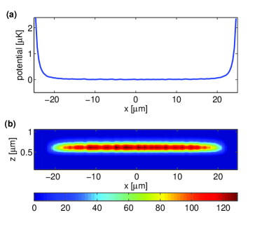
The trap depth, defined as the highest-energy isopotential that does not touch the surface, is about and is limited by the Casimir-Polder potential. An isopotential for a slightly higher energy is shown in Fig. 8(a). The radial frequency at the trap minimum is about , which is controllable over a wide range since we are passing such a modest current through the nanowire. The connecting legs of the Z-wire act as “end caps” for a waveguide potential that lies almost directly above the nanowire. Corresponding weighted tunneling probabilities are shown in Fig. 8(b) and (c). As was shown in Fig. 6(b), the tunneling lifetime due to the combined wire and surface Casimir-Polder potential is an order of magnitude shorter than that due to the wire Casimir-Polder potential.
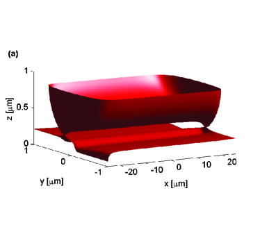
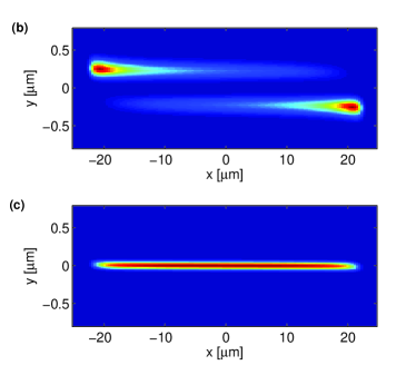
The trap formed for such small distances from the nanowire is “box” shaped along the longitudinal axis, as shown in Fig. 9(a). The smoothness of the trap bottom along the wire axis is limited only by the edge roughness of the nanowire (white-noise spectrum with rms, see Sec. III.1) and has a standard deviation of about . The effect of this corrugation on the ground state of trapped atoms is examined by solving the Gross-Pitaevskii equation for interacting bosons confined by the magnetic potential of the atomchip nanowire Dalfovo et al. (1999):
| (24) |
where is the atomic mass, is the external potential, the chemical potential, and is the atom-atom coupling constant, with being the s-wave scattering length ( for ). We do not use the Thomas-Fermi approximation since we do not expect a “large” number of atoms to be held in the trap. The calculated chemical potential for atoms of is = , which is about of the trap depth [Fig. 8(a)]. In Fig. 9(b) we present the calculated in-situ atomic density, which shows a standard deviation of 3.8% due to the nanowire edge corrugation effects. The isopotential plotted in Fig. 9(c) for an energy just above the minimum presents another view of the potential corrugation.
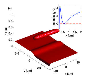
We see that a sufficiently deep trap can be formed using static magnetic potentials generated by nanowires, with sub-micron atom-surface separations. The main limitations for such traps will be cloud fragmentation and tunneling due to the Casimir-Polder potential. The latter limitation can be overcome using higher currents. For a wire, we can use a current up to [Fig. (2)]; at a height and a current , the trap depth increases to and the tunneling lifetime increases by many orders of magnitude. However, in this configuration the potential corrugation causes severe atomic density fragmentation, with a calculated standard deviation of 40%. In order to reduce the effects of potential corrugation, we can increase the chemical potential by shortening the nanowire trap. Shorter nanowires can actually be fabricated more easily and such traps would not be expected to significantly reduce the tunneling lifetime.
VII Anisotropic conductors
Replacing pure metals with other conductors such as superconductors, alloys or molecular conductors (see Introduction) may bring numerous advantages. As an example, we briefly describe utilizing electrically anisotropic materials and their qualities in the context of this work David et al. (2008). In particular, if we orient the “good” conductivity -axis parallel to the wire direction , the spatial and internal state decoherence rate of a trapped atomic sample is lowered by a factor on the order of the transverse conductivity suppression relative to gold, which may be several orders of magnitude. The greatest advantage of using such materials would therefore be for interferometric measurements with atomchips. The anisotropy in the resistance is also expected to decrease the effect of wire edge roughness on potential corrugations.
For a direct comparison with the gold Z-wire trap described above, we wish to maintain a current of through the trap. The -axis resistivity for these materials is typically larger than the resistivity of gold. For a material such as SrNbO3.41 the temperature of the wire at a current density of is not expected to rise significantly David et al. (2008), and hence the spin-flip lifetime due to thermal noise of the wire is expected to be about 200 times longer [Eq. (18)] than for the comparable gold nanowire. We note that this improvement is not due to the anisotropic nature of the wire but simply to its high resistivity (about 200 times that of gold). An additional factor of 2 may be gained for “one dimensional” anisotropic conductors due to the specific anisotropic nature of these wires David et al. (2008). Reducing the current density to (2 orders of magnitude smaller than that allowed in gold) requires a correspondingly increased wire cross-section of to maintain the same current. Following Fig. 6(a) this would reduce the above lifetime by a factor of about 20, ultimately yielding an increased spin-flip lifetime of a factor of .
Metallic nanowires have limited maximum current densities due to the increase in their wire resistivity (Fig. 2) from diffusive scattering at the wire surfaces. However, surface scattering for an anisotropic wire (where the surfaces are parallel to the good conductivity axis) may be significantly smaller and will have less effect on the wire resistivity, hence enabling higher current densities than discussed above. One may even speculate that at small dimensions the resistance relevant for the current density [Eq. (4)] and that relevant for the Johnson noise [Eq. (18)] may become decoupled.
It is evident that the behavior of electrons in anisotropic materials in the context of surface scattering (resistance) and edge currents (fragmentation) requires further theoretical and experimental study. In any case, it appears that utilizing anisotropic materials could further improve the advantages of nanowires. Specifically, it may improve the coherence time by several orders of magnitude, and could reduce potential corrugations David et al. (2008). Fabrication protocols for such anisotropic nanowires are being pursued in our laboratory.
VIII Summary and Conclusions
We have presented an analysis for further miniaturization achievable in atomchips based on current carrying wires, aiming to create static magnetic potentials capable of manipulating atoms on the scale of their deBroglie wavelength. We have analyzed the physical limitations of conducting wires, and we have also analyzed limiting effects due to the nearby surface, explicitly considering tunneling to the surface, surface thermal noise (causing both spin flips and decoherence), electron scattering within nanowires causing static potential corrugations, and the Casimir-Polder force. Additional effects such as Majorana spin flips have also been taken into account.
We have analyzed a specific example of a nanowire trap, utilizing a standard configuration. We have shown that when utilizing nanowires, the main limitations to trapping atoms at sub-micron atom-surface distances are potential corrugation and tunneling to the surface. We briefly described an anisotropic conductor as a potentially useful alternative to standard gold wires. These examples serve not only to summarize the more general statements of the paper, but also as an outlook for further work which may include alternative geometries and materials.
We have shown that further miniaturization of atomchips, utilizing wires with cross sections as small as a few tens of nanometers, enables robust operating conditions for atom optics. Such miniaturization may allow the realization of potentials (e.g., tunneling barriers) with a scale of the deBroglie wavelength, thereby bringing the atomchip a step closer to fulfilling its promise of a compact device for complex and accurate quantum optics with ultracold atoms. Achieving such small atom-surface distances should also contribute to the study of fundamental surface phenomena.
IX Appendix: Casimir-Polder potential – derivation
IX.1 A planar bilayer surface
We consider a planar structure with a dielectric function given by
| (25) |
The Green’s tensor for the EM field may be derived from the reduced Green’s tensor, which can be written as a sum over transverse modes with well defined transverse wave vectors
| (26) |
where in the region can be written in terms of transverse electric (TE) and transverse magnetic (TM) scalar Green’s functions
| (27) |
with . The reflection coefficients are given below. The first term in Eq. (27) is irrelevant, being cancelled by the vacuum subtraction in Eq. (14). The trace over the remaining part of the Green’s tensor is now given in terms of the (vacuum subtracted) scalar functions and at as
| (28) |
We now make the transformation such that with . The reflection coefficients and are now given by
| (29) |
for , where
| (30) |
and
| (31) |
with . We now obtain for the CP potential
| (32) |
The formulas for the multilayer Green’s functions have appeared in many places, for example in Ref. Klimchitskaya et al. (2000), and the result (32) was first derived by Zhou and Spruch Zhou and Spruch (1995).
At a distance which is much larger than , where is the lowest optical transition frequency of the atom, we may assume that . We now make the transformation and and obtain
| (33) |
with
| (34) |
where and are given in Eqs. (29)–(31) with replaced by and in the exponent replaced by .
When the exponent and one obtains and , which are the reflection coefficients for an interface between vaccum and a medium with dielectric function . On the other hand, when we obtain and . We conclude that the CP potential becomes similar to that generated by the deeper layer when and similar to the one generated by the outer layer when .
IX.2 Cylindrical wire
The Green’s tensor in cylindrical coordinates is given by Milton (2000)
| (35) |
where and are vectorial differential operators that generate the vector fields from the scalar fields for the TE and TM modes, respectively, is the two-dimensional Laplacian operator where the differentiation with respect to is replaced by , and are the scalar radial Green’s function for the TE and TM modes, respectively, and is the wave function that holds the angular and longitudinal dependence of each mode. As we are interested only in the single-point case and , we have here .
By substituting for the right forms of the Green’s function we obtain
| (36) | |||||
where and are the Bessel functions and the Hankel functions of the first kind and is the wave-vector along the radial direction. As above, we now make the transformation , such that with . The Bessel function transforms into , where is the modified Bessel function, and transforms into , the modified Bessel function of the second kind. We then obtain the following result:
| (37) | |||||
Now we take the static approximation for the polarizability and change variables to , and and find
| (38) | |||||
This can be written in the form
| (39) |
with
| (40) | |||||
The result of a numerical integration of is shown in Fig. 10. It is found that at , such that the atom is very close to the surface relative to the radius , we obtain the same result as for a plane conductor . In the other limit, where one may see that and the contribution to is dominated by the term only.
Acknowledgements.
We thank the team of the Ben-Gurion University Weiss Family Laboratory for Nanoscale Systems for the fabrication and characterization of the nanowires and the BGU AtomChip group for fruitful discussions. It is a pleasure to thank Carsten Henkel (Potsdam) for discussion and critical comments. This work was supported by the European Community “Atomchip” Research Training Network and the EC Marie-Curie programme, the American-Israeli Binational Science Foundation (BSF), the Israeli Science Foundation, the French Embassy in Israel, the German-Israeli Binational Science Foundation (GIF), and the Ministry of Immigrant Absorption (Israel). The work of K.A.M. is supported in part by grants from the US Department of Energy and the US National Science Foundation.References
- Folman et al. (2002) R. Folman, P. Krüger, J. Schmiedmayer, J. Denschlag, and C. Henkel, Adv. At. Mol. Opt. Phys. 48, 263 (2002).
- Reichel (2002) J. Reichel, Appl. Phys. B 75, 469 (2002).
- Fortágh and Zimmermann (2007) J. Fortágh and C. Zimmermann, Rev. Mod. Phys. 79, 235 (2007).
- Schumm et al. (2005) T. Schumm, S. Hofferberth, L. M. Andersson, S. Wildermuth, S. Groth, I. Bar-Joseph, J. Schmiedmayer, and P. Krüger, Nature Physics 1, 57 (2005).
- Jo et al. (2007) G.-B. Jo, J.-H. Choi, C. A. Christensen, Y.-R. Lee, T. A. Pasquini, W. Ketterle, and D. E. Pritchard, Phys. Rev. Lett. 99, 240406 (2007).
- Treutlein et al. (2004) P. Treutlein, P. Hommelhoff, T. Steinmetz, T. W. Hänsch, and J. Reichel, Phys. Rev. Lett. 92, 203005 (2004).
- Fortágh et al. (2002) J. Fortágh, H. Ott, S. Kraft, A. Günther, and C. Zimmermann, Phys. Rev. A 66, 041604(R) (2002).
- Jones et al. (2003) M. P. A. Jones, C. J. Vale, D. Sahagun, B. V. Hall, and E. A. Hinds, Phys. Rev. Lett. 91, 080401 (2003).
- Estève et al. (2004) J. Estève, C. Aussibal, T. Schumm, C. Figl, D. Mailly, I. Bouchoule, C. I. Westbrook, and A. Aspect, Phys. Rev. A 70, 043629 (2004).
- Wildermuth et al. (2005) S. Wildermuth, S. Hofferberth, I. Lesanovsky, E. Haller, L. M. Andersson, S. Groth, I. Bar-Joseph, P. Krüger, and J. Schmiedmayer, Nature 435, 440 (2005).
- Aigner et al. (2008) S. Aigner, L. D. Pietra, Y. Japha, O. Entin-Wohlman, T. David, R. Salem, R. Folman, and J. Schmiedmayer, Science 319, 1226 (2008).
- Emmert et al. (2009) A. Emmert, A. Lupaşcu, G. Nogues, M. Brune, J.-M. Raimond, and S. Haroche, Eur. Phys. J. D 51, 173 (2009).
- Dikovsky et al. (2005) V. Dikovsky, Y. Japha, C. Henkel, and R. Folman, Eur. Phys. J. D 35, 87 (2005).
- Trebbia et al. (2007) J.-B. Trebbia, C. L. GarridoAlzar, R. Cornelussen, C. I. Westbrook, and I. Bouchoule, Phys. Rev. Lett. 98, 263201 (2007).
- Fermani et al. (2007) R. Fermani, S. Scheel, and P. L. Knight, Phys. Rev. A 75, 062905 (2007).
- Japha et al. (2008) Y. Japha, O. Entin-Wohlman, T. David, R. Salem, S. Aigner, J. Schmiedmayer, and R. Folman, Phys. Rev. B 77, 201407(R) (2008).
- David et al. (2008) T. David, Y. Japha, V. Dikovsky, R. Salem, C. Henkel, and R. Folman, Eur. Phys. J. D 48, 321 (2008).
- Petrov et al. (2009) P. G. Petrov, S. Machluf, S. Younis, R. Macaluso, T. David, B. Hadad, Y. Japha, M. Keil, E. Joselevich, and R. Folman, Phys. Rev. A 79, 043403 (2009).
- Sukenik et al. (1993) C. I. Sukenik, M. G. Boshier, D. Cho, V. Sandoghdar, and E. A. Hinds, Phys. Rev. Lett. 70, 560 (1993).
- Lin et al. (2004) Y.-J. Lin, I. Teper, C. Chin, and V. Vuletić, Phys. Rev. Lett. 92, 050404 (2004).
- Obrecht et al. (2007) J. M. Obrecht, R. J. Wild, M. Antezza, L. P. Pitaevskii, S. Stringari, and E. A. Cornell, Phys. Rev. Lett. 98, 063201 (2007).
- Intravaia et al. (2007) F. Intravaia, C. Henkel, and A. Lambrecht, Phys. Rev. A 76, 033820 (2007).
- Ovchinnikov et al. (1991) Y. B. Ovchinnikov, S. V. Shul’ga, and V. I. Balykin, J. Phys. B 24, 3173 (1991).
- Schmiedmayer (1998) J. Schmiedmayer, Eur. Phys. J. D 4, 57 (1998).
- Shevchenko et al. (2004) A. Shevchenko, T. Lindvall, I. Tittonen, and M. Kaivola, Eur. Phys. J. D 28, 273 (2004).
- Rosenblit et al. (2006) M. Rosenblit, Y. Japha, P. Horak, and R. Folman, Phys. Rev. A 73, 063805 (2006).
- Ricci et al. (2007) L. Ricci, D. Bassi, and A. Bertoldi, Phys. Rev. A 76, 023428 (2007).
- Bender et al. (2009) H. Bender, P. Courteille, C. Zimmermann, and S. Slama, Appl. Phys. B 96, 275 (2009).
- Gillen et al. (2009) J. I. Gillen, W. S. Bakr, A. Peng, P. Unterwaditzer, S. Fölling, and M. Greiner, Phys. Rev. A 80, 021602(R) (2009).
- Peano et al. (2005) V. Peano, M. Thorwart, A. Kasper, and R. Egger, Appl. Phys. B 81, 1075 (2005).
- Dikovsky et al. (2009) V. Dikovsky, V. Sokolovsky, B. Zhang, C. Henkel, and R. Folman, Eur. Phys. J. D 51, 247 (2009).
- Roux et al. (2008) C. Roux, A. Emmert, A. Lupaşcu, T. Nirrengarten, G. Nogues, M. Brune, J.-M. Raimond, and S. Haroche, Europhys. Lett. 81, 56004 (2008).
- Mukai et al. (2007) T. Mukai, C. Hufnagel, A. Kasper, T. Meno, A. Tsukada, K. Semba, and F. Shimizu, Phys. Rev. Lett. 98, 260407 (2007).
- Cano et al. (2008) D. Cano, B. Kasch, H. Hattermann, R. Kleiner, C. Zimmermann, D. Koelle, and J. Fortágh, Phys. Rev. Lett. 101, 183006 (2008).
- Emmert et al. (2008) A. Emmert, A. Lupascu, G. Nogues, M. Brune, J.-M. Raimond, and S. Haroche, Eur. Phys. J. D 51, 173 (2008).
- Hänsel et al. (2001) W. Hänsel, J. Reichel, P. Hommelhoff, and T. W. Hänsch, Phys. Rev. A 64, 063607 (2001).
- Horikoshi and Nakagawa (2006) M. Horikoshi and K. Nakagawa, Appl. Phys. B 82, 363 (2006).
- Anderson (2009) D. Z. Anderson, private communication (2009).
- Rohrlich et al. (2006) D. Rohrlich, Y. Neiman, Y. Japha, and R. Folman, Phys. Rev. Lett. 96, 173601 (2006).
- Japha et al. (2007) Y. Japha, O. Arzouan, Y. Avishai, and R. Folman, Phys. Rev. Lett. 99, 060402 (2007).
- Fuchs (1938) K. Fuchs, Proc. Cambridge Philos. Soc. 34, 100 (1938).
- Sondheimer (1952) E. H. Sondheimer, Adv. Phys. 1, 1 (1952).
- Ashcroft and Mermin (1976) N. W. Ashcroft and N. D. Mermin, Solid State Physics (Hardcourt College publishers, 1976).
- Durkan and Welland (2000a) C. Durkan and M. E. Welland, Phys. Rev. B. 61, 14215 (2000a).
- Steinhögl et al. (2002) W. Steinhögl, G. Schindler, G. Steinlesberger, and M. Engelhardt, Phys. Rev. B. 66, 075414 (2002).
- Chambers (1950) R. G. Chambers, R. Soc. London, Ser. A 202, 375 (1950).
- Mayadas and Shatzkes (1970) A. F. Mayadas and M. Shatzkes, Phys. Rev. B 1, 1382 (1970).
- Durkan and Welland (2000b) C. Durkan and M. E. Welland, Ultramicroscopy 82, 125 (2000b).
- Groth et al. (2004) S. Groth, P. Krüger, S. Wildermuth, R. Folman, T. Fernholz, J. Schmiedmayer, D. Mahalu, and I. Bar-Joseph, Appl. Phys. Lett. 85, 2980 (2004).
- Casimir and Polder (1948) H. B. G. Casimir and D. Polder, Phys. Rev. 73, 360 (1948).
- Yan et al. (1997) Z.-C. Yan, A. Dalgarno, and J. F. Babb, Phys. Rev. A 55, 2882 (1997).
- Antezza et al. (2005) M. Antezza, L. P. Pitaevskii, and S. Stringari, Phys. Rev. Lett. 95, 113202 (2005).
- Henkel et al. (1999) C. Henkel, S. Pötting, and M. Wilkens, Appl. Phys. B 69, 379 (1999).
- Henkel and Pötting (2001) C. Henkel and S. Pötting, Appl. Phys. B 72, 73 (2001).
- Sukumar and Brink (1997) C. V. Sukumar and D. M. Brink, Phys. Rev. A 56, 2451 (1997).
- Henkel et al. (2003) C. Henkel, P. Krüger, R. Folman, and J. Schmiedmayer, Appl. Phys. B 76, 173 (2003).
- Dalfovo et al. (1999) F. Dalfovo, S. Giorgini, L. P. Pitaevskii, and S. Stringari, Rev. Mod. Phys. 71, 463 (1999).
- Klimchitskaya et al. (2000) G. L. Klimchitskaya, U. Mohideen, and V. M. Mostepanenko, Phys. Rev. A 61, 062107 (2000).
- Zhou and Spruch (1995) F. Zhou and L. Spruch, Phys. Rev. A 52, 297 (1995).
- Milton (2000) K. A. Milton, The Casimir Effect: Physical Manifestations of Zero-Point Energy (World Scientific, 2000).
- Leonhardt and Philbin (2007) U. Leonhardt and T. G. Philbin, New J. Phys. 9, 254 (2007).
- Munday et al. (2009) J. N. Munday, F. Capasso, and V. A. Parsegian, Nature 457, 170 (2009).
- Yannopapas and Vitanov (2009) V. Yannopapas and N. V. Vitanov, Phys. Rev. Lett. 103, 120401 (2009).