Probe and Control of the Reservoir Density of States in Single-Electron Devices
Abstract
We present a systematic study of quasi-one-dimensional density of states (DOS) in electron accumulation layers near a Si–SiO2 interface. In the experiments we have employed two conceptually different objects to probe DOS, namely, a phosphorus donor and a quantum dot, both operating in the single-electron tunneling regime. We demonstrate how the peaks in DOS can be moved in the transport window independently of the other device properties, and in agreement with the theoretical analysis. This method introduces a fast and convenient way of identifying excited states in these emerging nanostructures.
pacs:
73.21.-b,61.72.uj, 83.35.-pThe appearance of discrete energy spectra is often regarded as a fundamental property of quantum systems. However, the limit of vanishing energy spacing can be met in many mesoscopic systems at the interface of the quantum and classical regimes meaning that the energy levels can be treated as a continuum. This gives rise to the concept of density of states (DOS), the integral of which over an energy domain yields the number of quantum states in that region. The DOS concept has been successfully applied in explaining transport, absorption and emission, and quantum statistical phenomena in such devices Averin and Likharev (1991). In particular, DOS is a key element in the low-temperature behavior of metal-oxide-semiconductor field-effect transistors Ando et al. (1982) (MOSFETs) which constitute the cornerstone of information processing circuits today. Since device miniaturization has now reached the point where quantum effects of single atoms can dominate the operation characteristics Sellier et al. (2006); Calvet et al. (2007b); Lansbergen et al. (2008); Tan et al. (unpublished, 2009), there is an urgent need to understand and distinguish continuum DOS effects from the discrete quantum behavior. In this paper we present a systematic study of the reservoir DOS in two gated MOSFET nanostructures with quantum channels defined by either a quantum dot or the extreme case of a single donor atom.
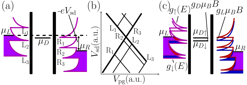
In a silicon MOSFET a positive gate voltage is applied to induce an electron layer directly below the Si–SiO2 interface. Hence, the electron dynamics is essentially limited to two dimensions, leading ideally to a constant DOS. In a narrow channel, however, the continuum approximation is only valid in the longest direction, giving rise to quasi-one-dimensional (Q1D) DOS with highly non-uniform characteristics, see Fig. 1(a). Conductance modulations attributed to Q1D density of states were first observed in a parallel configuration of 250 narrow MOSFET channels Warren et al. (1986) and later in a single channel Morimoto et al. (1995); Matsuoka et al. (1994); Takeuchi and Newbury (1990). Since the cumulative conductance through all occupied states was measured in these experiments, the studies were limited to rather low electron densities in the channel. The Q1D density of states is also intimately related to ballistic electron transport through quantum point contacts van Wees et al. (1988); Wharam et al. (1988), and has been probed in single carbon nanotubes using scanning tunneling microscopy Wildöer et al. (1998); Venema et al. (2000).

In single-electron transport through discrete quantum states Averin and Likharev (1991), the current is directly proportional to the reservoir DOS at a given energy, see Fig. 1. Considerable effort has been directed towards the study of local density of states of a reservoir in the vicinity of an impurity atom in a GaAs quantum well Holder et al. (1999); Schmidt et al. (1997, 1996). Here, the local DOS was dominated by disorder due to impurity scattering, resulting in reproducible but irregular features in the conductance which behaved in a complicated way as a function of magnetic field. Thus the term local DOS fluctuations was introduced. In our case, the behavior is less complicated, and hence we do not refer to peaks in DOS as fluctuations.
In gated devices, local DOS effects have also been observed in tunneling through a vertical quantum dot Kouwenhoven et al. (1997), for which a schematic stability diagram is shown in Fig. 1(b). Recently, gated quantum dots have attracted great interest due to their tunability, and lines in the stability diagrams not attributed to excited states have been observed in various structures Björk et al. (2004); Zwanenburg et al. (2009); Leturcq et al. (2009). In Refs. Zwanenburg et al. (2009); Leturcq et al. (2009) however, these lines were due to phonon modes, whereas in Ref. Björk et al. (2004) they were suggested to arise from reservoir DOS but were not studied thoroughly.
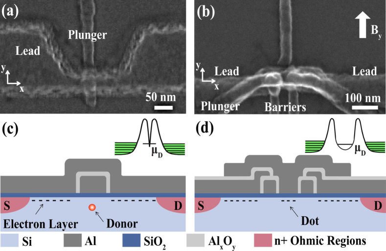
Motivated by the Kane proposal Kane (1998) for a quantum computer based on shallow donors in silicon Vrijen et al. (2000), there has been considerable development in electron transport through gated single donors Sellier et al. (2006); Calvet et al. (2007b); Lansbergen et al. (2008); Tan et al. (unpublished, 2009). In these experiments, conductance lines attributed to reservoir DOS have been observed but, again, not studied in detail. Indeed, it has not yet been proven that these features are due to the reservoir DOS. In this paper we present a systematic study of the reservoir DOS in two different nanostructures, namely, in a recently introduced double-gated single-donor transistor Tan et al. (unpublished, 2009) (Structure A) and in a novel multi-gated silicon quantum dot Lim et al. (2009) (Structure B), shown in Fig. 2. In contrast to previous studies of DOS, the double- and multi-gated designs allow us to map conveniently the reservoir DOS at a wide range of energies and electron densities.

The high-purity [001] silicon substrates for both device structures went through similar fabrication steps to those described in detail in Ref. Tan et al. (unpublished, 2009). In Structure B, however, there are three layers of metallic gates deposited with no implanted donors underneath. The working principle of both devices is that an accumulation layer of electrons is induced directly below the Si–SiO2 interface using the lead gate voltage . This layer constitutes the reservoirs for single-electron tunneling through a single donor or a quantum dot, the electrochemical potentials of which can be tuned by the plunger gate voltage . For Structure A, the plunger gate works also as a barrier gate, depleting the reservoirs in the vicinity of the donor. For Structure B, however, we have separate barrier gates which can be used to tune the coupling of the quantum dot to the left and right reservoir independently. The electron densities in the reservoirs can also be controlled independently, but for simplicity, we keep them at the same value here. As the plunger gate voltage is increased, the electrochemical potential of the donor or dot, , shifts down, eventually entering the source–drain bias window leading to single-electron tunneling through the device, see Fig. 1(a–b).
The sequential tunneling rate is directly proportional to the reservoir density of states, which leads to a peak in the source–drain current if is aligned with a peak in the density of states. Critically in our devices, we can shift the Fermi levels of the reservoirs with respect to the conduction band minima by changing the lead gate voltage, , which in turn moves the DOS peaks with respect to the transport window. The effect of the lead gate voltage on can be compensated by the plunger gate FN (1). Therefore, if we observe a conductance peak to shift with in the stability diagram, we can identify it to arise from a peak in the reservoir DOS, clearly distinct from features due to excited states in the dot or donor which do not move with . Previously, DOS peaks have been probed by changing the temperature Schmidt et al. (1996) or magnetic field Jouault et al. (2009), both of which also have an impact on the donor or the dot, and which are many orders of magnitude slower than the method presented here.
The measurements were carried out in 3He–4He dilution refrigerators below 100 mK temperatures. The conductance was measured using standard lock-in techniques and the direct current was measured from the same signal after low-pass filtering the modulation arising from the 10–50 V lock-in excitation. For Structure B, only the direct current was recorded and the differential conductance was extracted numerically.
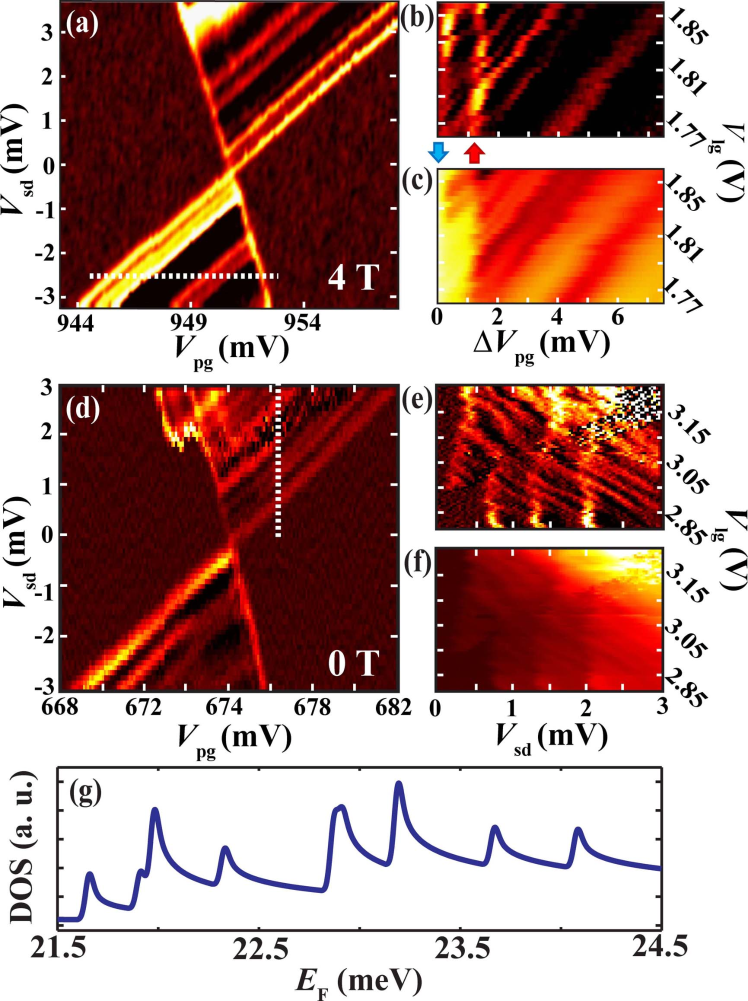
Figure 3 shows measured stability diagrams for Structure A [panel (a)] and B [panel (d)]. In Structure A the coupling of the donor to the left reservoir is much weaker than to the right reservoir, and hence only lines with positive slopes corresponding to the left reservoir are visible. This is justified by the sequential tunneling model, in which the current through the device is given by , where is the in/out-tunneling rate. Thus the current is determined by the small rate, independent of whether it corresponds to in- or out-tunneling. The tunneling rates in Structure B can be tuned to be symmetric, but considerable asymmetry persists in the working point of Fig. 3.

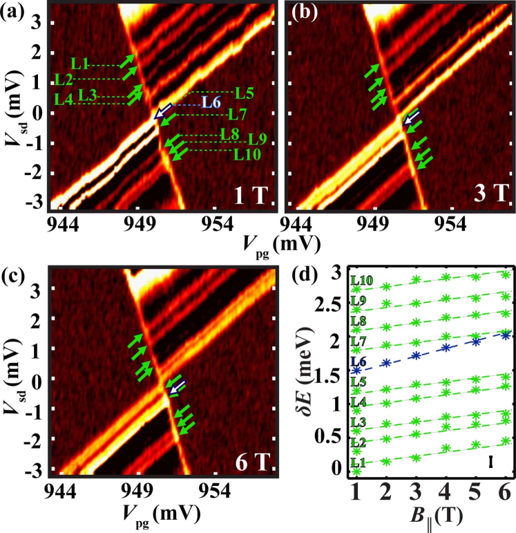
The stability diagrams shown in Fig. 3(a,d) do not provide enough information to distinguish whether a specific conductance feature is due to the reservoir DOS or an internal excited state. However, the lead-gate-compensated traces shown in Fig. 3(b,c,e,f) reveal the origin of the conductance peaks. Most of the peaks move with the lead gate voltage, and hence correspond to the reservoir DOS. However, Fig. 3(b,c) shows a feature meV above the ground state for all . As justified by measurements carried out in various magnetic fields (see Fig. 4), this line corresponds to the spin excited state of the neutral donor orbital ground state. Similarly, the vertical lines in Fig. 3(e,f) are attributed to excited states of the dot.
For Structure A, the slope of the DOS lines yields the response of the Fermi level to the lead gate voltage to be meV/V, where is the conduction band minimum. We have modeled this response using technology computer aided design tca taking into account the three-dimensional geometry of the system. By matching the measured response with the model, we obtain an estimate of the absolute value of the Fermi level to be meV.
The average energy spacing between the DOS peaks is obtained from Fig. 3 to be meV for Structures A and B. We model this by calculating the single-particle energy spectrum for a triangular well in the direction ( is the Heaviside step function), an infinite nm box potential in the direction, and a semi-infinite box potential in the direction. Here, is the electric field in the vicinity of the Si–SiO2 interface due to the lead gate. The one-dimensional DOS in the direction, for which the continuum approximation is valid, is given by , where is the effective mass of the electron in the direction. Thus we obtain for the total density of states
| (1) |
where , , and are the indices for the energy levels in the , , and valley degrees of freedom, respectively. The six-fold valley degeneracy of bulk silicon is lifted due to different effective masses and for the transverse and longitudinal directions, respectively Ando et al. (1982). Here, is the electron rest mass. Thus the effective mass in the direction depends on the valley degree of freedom. According to Eq. (1), a peak in DOS is observed at energies matching the single-particle energy levels in the two-dimensional potential, i.e., for .
The peak spacing resulting from the confinement in the direction is given by . This yields the minumum peak spacing of 1.2 meV for the transverse and 0.25 meV for the longitudal effective masses. Each excited state in the valley and degree of freedom superimposes an additional series of peaks, and hence the resulting DOS structure can be rather complicated. Figure 3(g) shows the DOS in the vicinity of the Fermi level obtained above for Structure A. The electric field of is chosen to be MV/m to match the peak separation observed in the experiments. This field is approximately an order of magnitude lower than expected due to the crude model used to calculate the peak spacing. This simple model does not include the true details of the trapping potential including disorder or the electric field induced by the accumulation layer, which calls for deeper theoretical analysis. Furthermore, we have not included the possible splitting of all valley degeneracies which would further reduce the average peak spacing and consequently, increase the required electric field.
Figure 1(c) shows a schematic diagram of how the DOS peaks behave in magnetic field . The Zeeman effect shifts the kinetic energy at the Fermi level () for the spin-down electrons up by , and vice versa for spin-up electrons. Here, is the electron factor in the reservoirs and . Thus the effect of this term is to shift and split the DOS peaks. However, if the electron factor for the donor or dot, , is almost the same as , this compensates for the splitting and results only in a downwards shift of the DOS peaks by with respect to the transport window. In our case, the DOS peaks simply shift and do not split in magnetic field, as demonstrated in Fig. 4, which implies consistent with previous measurements Willems van Beveren et al. (2008). In contrast, Zeeman splitting of DOS peaks has been observed in tunneling through a Si shallow donor in a GaAs/AlAs/GaAs junction Jouault et al. (2009).
Figure 4(d) shows the energy shift of the conductance peaks with respect to the transport window as a function of magnetic field. We observe that within the estimated error, the shift of the DOS peaks and the spin excited state is in agreement with and , respectively. Thus our observations can be explained by the Zeeman effect alone.

In conclusion, we have reported the first studies of reservoir DOS in nanostructures through gate control of the reservoir electron density. Magnetic field spectroscopy of the DOS peaks revealed behavior consistent with energy shifts due to the Zeeman effect alone. Both the single donor and the quantum dot devices studied exhibited similar conductance patterns arising from the reservoir DOS. Our findings not only confirm the interpretation that additional conductance lines observed previously in transport through single donors are due to reservoir states Sellier et al. (2006); Lansbergen et al. (2008); Tan et al. (unpublished, 2009), but also demonstrate that these states can be controlled and studied in a quantitative manner.
The authors thank F. Hudson, D. Barber, and R. P. Starrett for technical support, E. Gauja, A. Cimmino, and R. Szymanski for assistance in nanofabrication, and M. Eriksson, J. P. Pekola, and V. Pietilä for insightful discussions. M. M. and J.-M. P. acknowledge Academy of Finland, Emil Aaltonen Foundation, and Finnish Cultural Foundation for financial support. This work is supported by the Australian Research Council, the Australian Government, the U.S. National Security Agency (NSA), and the U.S. Army Research Office (ARO) (under Contract No. W911NF-08-1-0527).
References
- Averin and Likharev (1991) D. V. Averin and K. K. Likharev, In Mesoscopic Phenomena in Solids, Edited by B. L. Altshuler, P. A. Lee, and R. A. Webb (Elsevier, Amsterdam, 1991), pp. 173.
- Ando et al. (1982) T. Ando et al., Rev. Mod. Phys. 54, 437 (1982).
- Sellier et al. (2006) H. Sellier et al., Phys. Rev. Lett. 97, 206805 (2006).
- Calvet et al. (2007b) L. E. Calvet et al., Phys. Rev. Lett. 98, 096805 (2007b).
- Lansbergen et al. (2008) G. P. Lansbergen et al., Nature Phys. 4, 656 (2008).
- Tan et al. (unpublished, 2009) K. Y. Tan et al., arXiv:0905.4358 (unpublished, 2009).
- Warren et al. (1986) A. C. Warren et al., Phys. Rev. Lett. 56, 1858 (1986).
- Morimoto et al. (1995) K. Morimoto et al., Jpn. J. Appl. Phys. 35, 853 (1995).
- Matsuoka et al. (1994) H. Matsuoka et al., J. Appl. Phys. 76, 5561 (1994).
- Takeuchi and Newbury (1990) K. Takeuchi and R. Newbury, Phys. Rev. B 43, 7324 (1990).
- van Wees et al. (1988) B. J. van Wees et al., Phys. Rev. Lett. 60, 848 (1988).
- Wharam et al. (1988) D. A. Wharam et al., J. Phys. C 21, L209 (1988).
- Wildöer et al. (1998) J. W. G. Wildöer et al., Nature 391, 59 (1998).
- Venema et al. (2000) L. C. Venema et al., Phys. Rev. B 62, 5238 (2000).
- Holder et al. (1999) J. P. Holder et al., Phys. Rev. Lett. 84, 1563 (1999).
- Schmidt et al. (1997) T. Schmidt et al., Phys. Rev. Lett. 78, 1540 (1997).
- Schmidt et al. (1996) T. Schmidt et al., Europhys. Lett. 36, 61 (1996).
- Kouwenhoven et al. (1997) L. P. Kouwenhoven et al., Science 278, 1788 (1997).
- Björk et al. (2004) M. T. Björk et al., Nano Lett. 4, 1621 (2004).
- Zwanenburg et al. (2009) F. A. Zwanenburg et al., Nano Lett. 9, 1071 (2009).
- Leturcq et al. (2009) R. Leturcq et al., Nature Phys. 5, 327 (2009).
- Kane (1998) B. Kane, Nature 393, 133 (1998).
- Vrijen et al. (2000) R. Vrijen et al., Phys. Rev. A 62, 012306 (2000).
- Lim et al. (2009) W. H. Lim et al., arXiv:0910.0576 (2009).
- FN (1) An increment in the lead gate voltage also results in a slight increase of the transparency of the tunnel barriers. In Structure B, this can be compensated by decreasing the voltage on the barrier gates.
- Jouault et al. (2009) B. Jouault et al., Phys. Rev. B 79, 041307(R) (2009).
- (27) Technology Computer Aided Design modeling package, Integrated Systems Engineering AG, Zurich.
- Willems van Beveren et al. (2008) L. H. Willems van Beveren et al., Appl. Phys. Lett. 93, 072102 (2008).