A Consistent Picture of the Charge Distribution in Reduced Ceria Phases
Abstract
We consider the implications of the bond valence model (BVM) description of charge distribution in reduced ceria phases (CeO2-x)[1, 2] to the models used to describe electronic and ionic conductivity in these phases. We conclude that the BVM is consistent with both the small polaron model (SPM) and the atomistic models which describe the electronic and ionic conductivities respectively. For intermediate phases, i.e., , we suggest the possibility of low temperature metallic conductivity. This has not yet been experimentally observed. We contrast the BVM results and the conventional description of charge distribution in reduced ceria phases.
keywords:
Cerium Oxides, Rare Earths, Electronic conductivity, Ionic Conductivity, Small Polaron Model, Conducting Materials, Bond Valence Model, Atomistic ModelsIntroduction
Ceria is a technologically important material with applications in high temperature electrochemical devices [3, 4, 5, 6, 7], catalysis [8, 9, 10, 11] and oxygen gas sensors [12, 13]. It is the capacity of ceria to rapidly take up and release oxygen that makes it valuable for these applications. The process can be described by a reversible chemical reaction:
| (1) |
The oxygen exchange controls both the electronic and ionic conductivities in reduced phases, CeO2-x, and both channels of charge transport are important in typical applications. This is illustrated by the example of a solid-oxide fuel cell where ceria forms the anode. The oxidation of the fuel takes place on the anode and involves the abstraction of lattice O from the ceria. When an O atom is removed, a vacancy site results and two extra electrons are left in the crystal lattice of the anode. For the fuel cell to operate, two processes must ensue. First, the electrons move to the cathode through an external circuit, which relies on the electronic conductivity of the ceria. Second, oxide ions migrate from the bulk to the surface of the anode where the chemical reaction occurs, which requires a sufficiently large ionic conductivity.
A description of the charge distribution in stable structures of CeO2-x may elucidate the microscopic mechanism of both the electronic and ionic conductivities. For a long time, it was widely held that when an O vacancy forms in bulk ceria, the associated charge localizes on two of the nearest neighbour Ce sites [14, 15, 16, 17, 18]. We will call this the standard picture. Recent results from atomistic simulations challenge this view, indicating that dopant ions prefer to occupy the second or third coordination shell of the O vacancy [19, 20, 21, 22]. These reports are consistent with our own results from the BVM for slightly reduced ceria [1, 2], which also contradict the standard picture.
In Fig. 1, we summarize the results of the standard picture and the BVM.
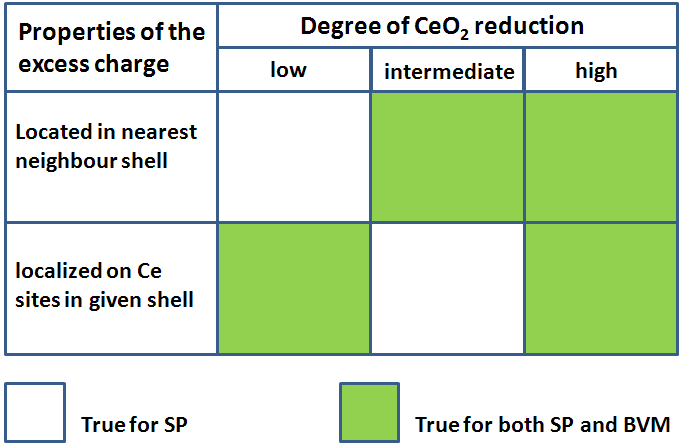
In the standard picture, the two extra electrons localize in the nearest neighbour shell for all compositions of reduced ceria. The results of the BVM are different for different composition ranges of the reduced ceria phases (i.e. for different ranges of in CeO2-x). We roughly define ‘low’, ‘intermediate’ and ‘high’ -vacancy concentration ranges according to , and , respectively. In the low range, the BVM predicts that the two extra electrons localize in the next nearest neighbour shell; in the intermediate region, they delocalize in the nearest neighbour shell while in the high region, the result is the same as that for the standard picture.
Except for fully reduced ceria, the standard picture and the BVM give qualitatively different descriptions of charge distribution in CeO2-x phases. We aim to determine whether the difference in charge distributions results in a corresponding difference in the transport properties of these materials. We thus study the electronic and ionic conductivities of the material using appropriate models of charge transport, and ask how the charge distribution will affect model predictions.
In Section 1 we provide theoretical background on electronic and ionic conductivity in doped ceria. We apply these results to study experimental data on the electronic conductivity in the low and intermediate reduction regimes in Sections 2 and 3, respectively. The ionic conductivity is examined in Section 4. In Section 5 we conclude.
1 Theory
Towards understanding general properties of electronic conductivity in reduced ceria we start with a review of the electronic band structures of CeO2 and Ce2O3, which correspond to extremal oxidation states of the Ce oxides. We then go on to describe the phenomenology of incoherent electron mobility in CeO2-x phases and the relationship between carrier and electronic structure. It turns out that the ionic mobility, described as a process of O vacancy migration, has similar properties to incoherent electron mobility. Thus, an important question is how the two types of charge carriers might be distinguished experimentally.
1.1 Electronic Band Structures of CeO2 and Ce2O3
CeO2 and Ce2O3 are insulators for entirely different reasons. As can be seen from Fig. 2(a), CeO2 is a band insulator with a band gap of . The valence band is of mainly O character while the conduction band consists predominantly of the Ce states. Since there is a negligible probability for electrons to be thermally excited from the valence band to Ce states at relevant temperatures, there is no electronic conductivity in stoichiometric CeO2. In slightly reduced ceria, electronic conductivity involves the states. The latter exist within a narrow band and thus describe electrons that are approximately localized on individual Ce sites. Electron hopping between these sites involves a phonon-assisted mechanism. This process is thermally activated at temperatures below 1000 K or so (a value typical of working device conditions).
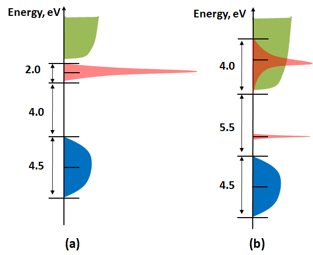
In contrast, Ce2O3 is a Mott insulator [26, 23]. The Ce states are partially occupied with one electron per site. If the Coulomb repulsion between electrons was taken to be weak, then band theory would predict the system to be a metal. However, the compact states have a high on-site Coulomb repulsion, , which prohibits the double occupancy of a site. Since electronic conductivity would require that an electron hops onto a Ce site which is already occupied, this material is an insulator with a band gap related to . Fig. 2 shows that the band gap between the filled valence band and the conduction band is and that between the partially occupied Ce states and the conduction band is . Since is larger than this energy gap, it is more likely for the electrons to be thermally excited into the conduction band than doubly occupying the local orbitals. In any case, the number of free carriers is small at relevant temperatures. At low temperatures, the small polaron model (SPM) has been used to describe electronic conductivity in reduced ceria phases [29]. We now briefly review the main features of this model.
1.2 The Phenomenology of Charge Carrier Mobility in CeO2-x Phases
The electronic mobility can be equivalently described within two theoretical formalisms: the SPM of Holstein [30, 31, 29] and the Marcus-Hush theory [32, 33]. To model the ionic mobility, we consider O vacancy migration or O self-diffusion in the CeO2-x phases [34, 35, 36].
The fact that electronic mobility in reduced ceria is activated means that the mathematical description of electronic and ionic charge transport is similar (unlike in a metal, where there is no activation barrier to electronic mobility). We take advantage of this correspondence below, while being careful to point out the significant differences between electronic and ionic transport that remain.
We define a vacancy cluster consisting of the vacancy together with all the atoms up to and including the nnn Ce sites. Ionic conductivity involves the migration of the vacancy cluster on the O sublattice. The occupied O-lattice sites (so called normal sites) and the vacancy sites are assumed to be energetically inequivalent with the difference in energy given by , Fig. 3(a). Similarly, to describe electronic hopping on the cationic sublattice, we assume two types of Ce sites - the Ce3+ and Ce4+ which are energetically inequivalent. The energy difference between these sites is , Fig. 3(b).
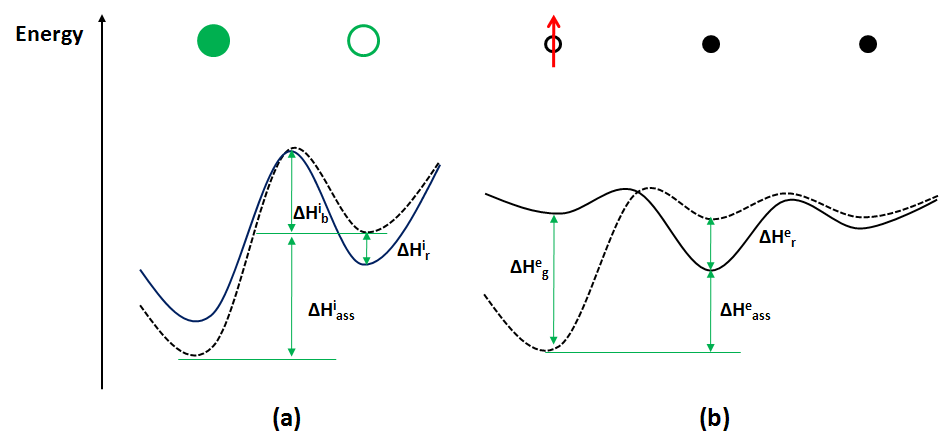
To mobilize a charge carrier requires that its associated energy barrier be overcome, so an energy of at least , for electrons, or , for ions, must be provided by thermal fluctuations. In the case of ionic conductivity there is an additional barrier energy, , associated with O2- jumping to the saddle point at the boundary of the first coordination shell of Ce ions. Once the O2- reaches the vacancy site, the lattice relaxes to the new configuration. The lattice relaxation has an associated energy, . Thus the mobility barrier of an O ion is given by the sum: . For electronic conductivity, no barrier energy analogous to exists so only the energy need be provided for the electron can tunnel to a neigbouring Ce site. However, as in the ionic case, once the electron transfer has occurred, the lattice relaxes with an energy given by . Consequently, the mobility energy of an electron is given by: .
For a mixed conductor with several charge carriers, the total conductivity is given by:
| (2) |
where , , and refer to the conductivity, density, charge and mobility of the th species of charge carrier. The O vacancies and/or electrons are bound to the O vacancy cluster so to obtain ‘free’ charge carriers, energy corresponding to at least and must be provided to the system for vacancies and electrons respectively. The thermally activated free carrier population is given by
| (3) |
where is the Boltzmann constant and is the temperature. For itinerant electrons, the mobility is given by:
| (4) |
where and are the electron charge and mass and is the mean free time for electron scattering. For SPM and ionic conductivity, the mobility is diffusive and activated. It is related to the diffusivity, , by the Nernst-Einstein relation [36]:
| (5) |
A general expression for the diffusion coefficient,, is obtained from random walk theory which assumes uncorrelated motion of the charge carriers. It is found that this expression has the same form for both SPM electronic [29] and ionic [34, 37, 4] conductivity given by:
| (6) |
where the quantity, , has a different meaning between electronic and ionic conductivity as will be described below. The quantity, , is the concentration of normal sites, i.e., sites which are occupied by O atoms for ionic conductivity, and by Ce3+ ions for SPM conductivity. Hence with and being the numbers of occupied and total available sites of type respectively. The attempt frequency, is reported to be for ionic conductivity [34] and for SPM electronic conductivity [29] which corresponds to the optical mode vibration frequencies.
Finally, the quantity, , for the case of ionic conductivity is given by:
| (7) |
with being the coordination number in the O sublattice of the site from which the O ion hops. For slightly reduced CeO2, has the same value as it does in the unreduced phase so that . For the electronic case, the value of depends on whether the electron transfer is adiabatic or non-adiabatic[30, 31, 29]:
| (8) |
Here, is the electron hopping matrix matrix element and is the reorganization energy.
For the motional free energy, we have already noted the energy terms that enter into the calculation of for both ionic and electronic conductivity. From Eqs. 6, 5, 3 and Eq. 2 we get:
| (9) |
where,
| (10) |
| (11) |
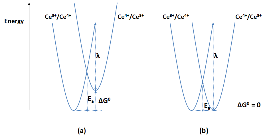
Small polaron (SP) electron transfer can be equivalently described in the Marcus-Hush theory which provides a general expression for the calculation of the rate of electron transfer [32]:
| (12) |
where is the electron transfer rate or jump frequency (), and is the Gibbs free energy of the electron transfer reaction. This model of electron transfer enables us to calculate from some experimental data on mobility and activation energies.
The electron transfer rate, , is related to the diffusion coefficient [38, 39, 40]:
| (13) |
Here, is the number of equivalent nearest neighbour sites onto which the electron can hop and is the jump distance. As we only have experimental data of mobilities for slightly reduced ceria, we consider the Ce sublattice to be that of CeO2 so that and , where is the lattice constant.
The activation energy and the reorganization energy are related to each other by:
| (14) |
Fig. 4 is a simple schematic of how SP transport in CeO2-x phases can be viewed in the Marcus-Hush picture (See also Fig. 7.8 in Mahan [41]).
1.3 Parameters for Conductivity in CeO2-x Phases
We summarise in Table 1 both experimental and theoretical results for the main parameters in the conductivity equation, Eq. 9, in both the electronic and ionic cases.
| Electronic | Ionic | ||||||
|---|---|---|---|---|---|---|---|
| Ref. | Ref. | ||||||
| [43] | [43] | ||||||
| [29] | [44, 45, 42] | ||||||
| [46] | [47] | ||||||
| 111obtained for Sm-doped ceria: Ce0.85Sm0.15O1.925-δ (SDC15) | [48] | 111obtained for Sm-doped ceria: Ce0.85Sm0.15O1.925-δ (SDC15) | [48] | ||||
| 222obtained for Gd-doped ceria: Ce0.9Gd0.1O1.95-δ (GDC10) | [5] | 222obtained for Gd-doped ceria: Ce0.9Gd0.1O1.95-δ (GDC10) | [5] | ||||
| 333obtained for Gd-doped ceria: Ce0.8Gd0.2O1.9-δ (GDC20) | [49] | 333obtained for Gd-doped ceria: Ce0.8Gd0.2O1.9-δ (GDC20) | [49] | ||||
1.4 Signatures of Hopping Conductivity
Table 1 shows that the motional enthalpy for electronic conductivity is . The fact that the electronic conductivity is activated is consistent with incoherent (hopping) transport associated with localized charge. However, the activation energy is much less than the energy gap from the states to the delocalized band in these materials which, e.g., in CeO2 is (compare Fig. 2).
SP transport can also be investigated by measurement of the Seebeck coefficient of a material. In this case, the temperature dependence of the Seebeck coefficient is used to determine whether or not hopping mobility exists. We have noticed that mainly two models have been used in the literature to describe the Seebeck coefficient of SP transport. The first one is more applicable to broad band semiconductors and shows a temperature dependence [50, 51]:
| (16) |
where is a coefficient of order unity. Eq. 16 is valid at low to moderate temperatures, i.e., . At high temperatures, the Heikes formula, which is temperature-independent should be used [52, 53]:
| (17) |
Chaikin and Beni argue that Eq. 16 should not be used for narrow band materials as it does not describe localized states well [53].
1.5 Decoupling the ionic from the electronic conductivity
Both the Hall and Seebeck coefficients have the same sign as the charge carrier and so can be used to establish the type of charge carrier involved. A negative Seebeck coefficient was reported by Tuller and Norwick [29] implying that the electrons are the majority carriers for compositions where in CeO2-x.
Another method to distinguish between electronic and ionic conductivities is impedance spectroscopy [48]. Here, a Nyquist plot of the the impedance spectrum gives the so-called ‘half tear-drop’ profile for a mixed conductor which arises from two charge carriers with different time constants being superimposed on the same curve. The results of Lai and Haile [48] appear to corroborate the finding by Tuller and Norwick [29] that electrons are the majority carriers in slightly reduced ceria. However, comparison of the two sets of results is not a simple matter as the former researchers used Sm-doped ceria whereas the latter used slightly reduced ceria.
2 Electronic Conductivity in Slightly Reduced CeO2-x Phases
Experimental work on electronic charge transport in the CeO2-x phases has been interpreted in terms of the small polaron model [46, 29]. Tuller and Norwick found a reasonable fit to Eq. 17 for the Seebeck coefficient of the CeO2-x phases [29]. Within the small polaron description the propagation of the charge carrier through the lattice is associated with a propagation of a lattice distortion. There is no reason why the polaron must be confined to the vicinity of the oxygen vacancy. It was shown in Ref. [2] from the BVM analysis that most of the excess charge in the crystal of Ce11O20 is localized on next nearest neighbour Ce sites from the O vacancy. In the same report, a prediction was also made that all the excess charge in Ce6O11 should be localized on the next nearest neighbour Ce sites. Thus, we see that the charge distributions obtained from the BVM do not contradict the SPM for small values of and we can make a connection between the two pictures. The transport data can be used to obtain an estimate of the hopping matrix element, , from Eq. 15 using for the lattice constant we find:
| (18) |
An estimate of can also be obtained from the Harrison method (see Section 3) which gives . The bandwidth of the level in CeO2, , calculated from density functional theory (DFT) is [27, 25]. The bandwidth is related to the hopping integral by so we have in agreement with the result from the Harrison method. In contrast, the value of in Eq. 18 appears too low. However, since is also thermally activated, the mobility cannot be accurately determined from fits over a small temperature range. Moreover, correlation effects might be important in reducing the effective mobility.
3 Electronic Conductivity in CeO2-x Phases at Intermediate Reduction
We now consider the electronic conductivity in phases of intermediate reduction. We discuss the example of Ce7O12. Since the charge distribution obtained from the BVM suggests a delocalization of the charge on the Ce(2) sublattice [1, 2], we include calculations of the hopping matrix elements by the Harrison method [54]. The results enable us to discuss the question of charge delocalization in this crystal in a somewhat quantitative way.
A key structural unit for discussing the electronic conductivity in this crystal is the divacancy cluster shown in Fig. 5. It results from the removal of two O atoms from the parent fluorite structure of CeO2. Two distinct Ce sites are obtained; the site with two nearest neighbour O vacancies and the site with only one O vacancy neighbour. The site has been called the divacancy site [55] and it forms a shared corner between two coordination tetrahedra of the O vacancies as illustrated in Fig. 5.
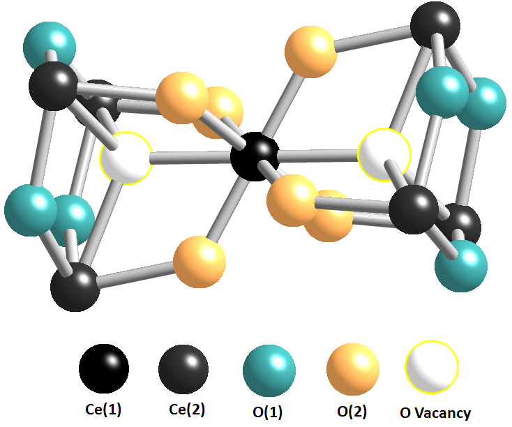
If we consider one of the O vacancies in the divacancy, the bond valence results indicate that the charge delocalizes among the Ce(2) sites that form an equilateral triangle. As different triangles are connected by relatively short Ce-O bonds, it is plausible that charge is delocalized throughout the entire crystal on the Ce(2) sublattice. If this is the case, we can discuss the low temperature electronic conductivity of Ce7O12 based on a simplified picture of a system of connected equilateral triangles each with a delocalized charge at one-third filling. We can disregard the Ce(1) sites because the electrons from the O vacancy do not occupy these sites. It is probably the case that a large activation energy is associated with the hopping of an electron onto Ce(1) sites.
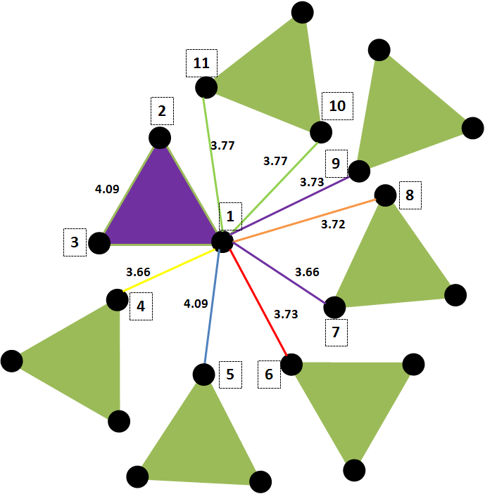
Fig. 6 shows a schematic of this simplified model where we have also included the direct Ce-Ce distances to give an indication of the relative separation between the equilateral triangles. We see that the distances between the triangles range from to . The latter is the intra-triangle distance. Thus, inter-triangle distances are shorter or equal to the intra-triangle distances and thus the inter-triangle electron hopping matrix element may be comparable to the intra-triangle matrix element.
The direct Ce-Ce distances are summarised in Table 2 along with the matrix elements for direct - coupling between neighbouring Ce sites, . Table 2 shows that all but one of the matrix elements for inter-triangle electron hopping are larger than the intra-triangle value of . The electron hopping matrix elements between lattice sites, were calculated from Harrison’s method of universal parameters [54].
Since electrons may become delocalized on the Ce lattice by indirect hopping via oxygen sites we also should consider relevant Ce-O bond distances. Fig. 7 shows the Ce-O bond lengths associated with the bonding of the Ce1 site to its ten nearest neighbour Ce sites. The Ce-O bonds are summarized in Table 2 together with the matrix elements for electron hopping between Ce sites via an O site, i.e., -- hopping, . Indirect hopping between two Ce(2) sites via an intervening O site involves a two-step process in which the electron first hops from the first Ce(2) to the O site and then from the O site to the second Ce(2) site. If is the matrix element for hopping between a Ce(2) site and an O site, the overall matrix element for the electron hopping between two Ce(2) sites via an O site, , is then given by Eq. (19):
| (19) |
where is the energy gap between the Ce - and the O levels, which, in the calculation, we assume to be . The matrix elements for indirect electron hopping given in Table 2 are calculated from this formula [54, 56, 57]. We note that all the matrix elements listed in Table 2 are for the - interaction between the two orbitals as they are the most favourable.
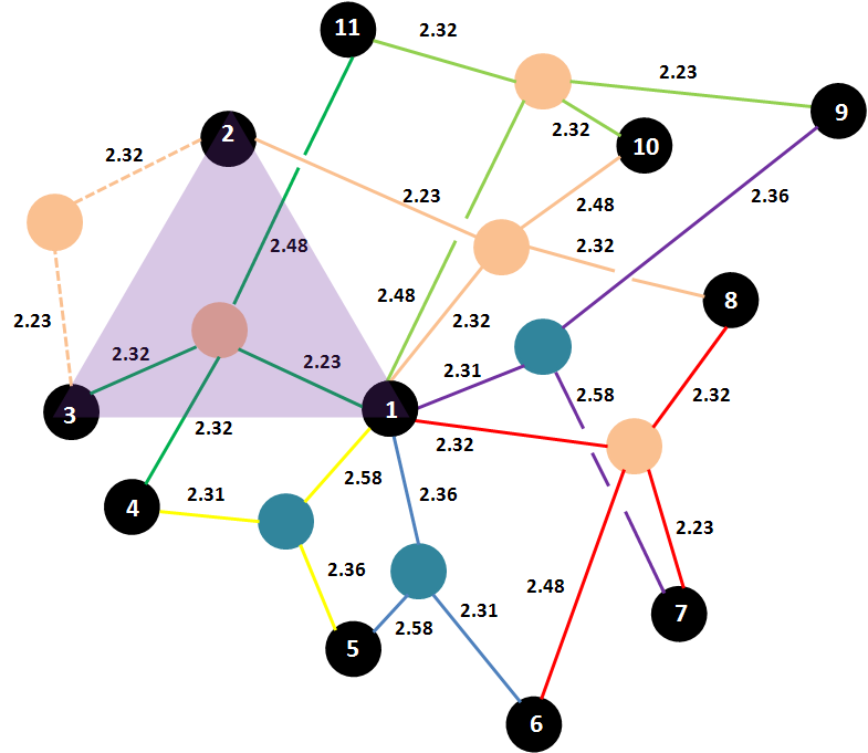
From Table 2, we see that the matrix elements for intra-triangle hopping are equal and have the value . The same value is obtained for electron hopping from the Ce1 site to the Ce4 and Ce7 sites. An electron at Ce1 has an equal probability of hopping onto sites Ce2 and Ce3 (intra-triangle hopping) or onto sites Ce4 and Ce7 (inter-triangle hopping). The matrix elements for an electron at Ce1 to hop to Ce8 are also similar. If these matrix elements are a fair indicator of the tendency towards charge delocalization, then they support our conjecture that the charge should be delocalized throughout the Ce(2) sublattice of Ce7O12. This delocalization of charge throughout the crystal would imply that Ce7O12 should exhibit metallic conductivity at low temperature. If this is true, then Ce7O12 should have the highest low-temperature electronic conductivity of all the reduced phases of ceria.
We have not found any reports of low temperature electronic conductivity measurements of Ce7O12.
| Cei | Ce1-O, | O-Cei, | Ce1-O-Cei distance, | , | Ce1-Cei distance, | , |
|---|---|---|---|---|---|---|
| Ce2 | ||||||
| Ce3 | ||||||
| Ce4 | ||||||
| Ce4 | ||||||
| Ce5 | ||||||
| Ce5 | ||||||
| Ce6 | ||||||
| Ce6 | ||||||
| Ce7 | ||||||
| Ce7 | ||||||
| Ce8 | ||||||
| Ce8 | ||||||
| Ce9 | ||||||
| Ce9 | ||||||
| Ce10 | ||||||
| Ce10 | ||||||
| Ce11 | ||||||
| Ce11 |
But some results for Pr7O12 and Tb7O12 may be applicable. In a study of the electrical conductivities of PrO2-x and TbO2-x, Rao et al. [58] found the highest conductivities for the compositions corresponding to Pr7O12 and Tb7O12. The authors also found that the Seebeck coefficient vanished at this composition. It was suggested that the seven-coordinated cations with an average charge of would be responsible for the observed high conductivity. We, however, emphasize here that the results of Rao et al. are for electronic conductivity at temperatures - whereas the bond valence results are for low temperature. Electronic conductivity at high temperature may be dominated by electron-phonon coupling effects which are absent at low temperature.
We did not find any report on the electronic conductivity of reduced ceria at the exact composition corresponding to Ce7O12. The results of Tuller and Nowick [29] reproduced in Fig. 8 are the closest we got.
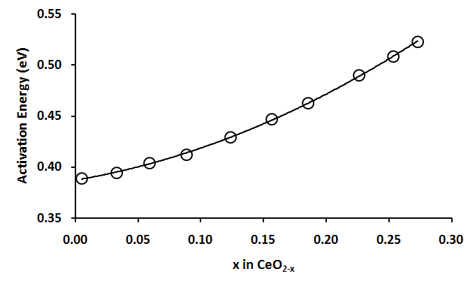
The data in Fig. 8 which support the SPM shows an increase in the activation energy for the electron hopping with increasing to about which is the upper limit of the composition range measured. An extrapolation of these results to the composition of Ce7O12 () would suggest a higher activation energy for electron hopping. However, it is not clear whether or not an extrapolation is a valid extension in the interpretation of these data. As the authors pointed out, it is expected that at this composition, an transition will occur which may invalidate any extrapolative interpretation. Thus the situation regarding Ce7O12 appears somewhat inconclusive from the data on the SPM we were able to find. That low temperature metallic conductivity (i.e. band transport) should occur in Ce7O12 is unexpected from a consideration of the electronic structures of CeO2 and Ce2O3. These two phases are relatively well characterized and form the boundaries of the CeO2-x composition range. On this composition range, Ce7O12 is closer to Ce2O3 than it is to CeO2. CeO2 is a band (charge transfer) insulator whereas Ce2O3 is a Mott insulator. The crossover from incoherent (hopping) to coherent (band) transport will occur at a temperature such that .
4 Results from Atomistic Models for Ionic Conductivity in CeO2-x Phases
There is a large body of literature on the study of ionic conductivity in doped ceria [59, 4, 6, 60, 61, 62, 63, 64]. It is known that the local crystal environment of the O vacancies affects their mobility, so defect cluster models that simulate the local environment of the defect are employed. Below, we review some key results of the literature and consider whether they are consistent with the BVM.
The mechanism of bulk ionic conductivity in doped or reduced ceria can be viewed either as oxygen self-diffusion or vacancy diffusion (of course, oxygen atoms move in the opposite direction to oxygen vacancies) under an applied electric field. The ionic conductivity is proportional to the product of the charge and concentration of the carriers and has an Arrhenius temperature dependence with an activation energy [65, 66, 67].
The process of doping CeO2 with a trivalent oxide, M2O3, can be described by:
| (20) |
where M is a dopant ion on a Ce4+ site. Note that for M=Ce, Eq. 20 is equivalent to reduction of CeO2, Eq. 1. For free O vacancies, the conductivity at low temperature is described by Eq. 10 with , so the ionic conductivity is a linear function of the O vacancy (and hence dopant) concentration provided that and are approximately constant. However, experimental observations show that both and are highly nonlinear functions of the dopant concentrations, which means that a concentration dependence of should be assumed if Eq. 10 is to be used.
To explain the relationship between and dopant concentration, O vacancy cluster models were proposed. In these so-called defect associate models, the O vacancies are bound to the dopant ions and form stable associates of the the form and . The latter is a neutral cluster which is only relevant at high dopant concentrations. Note that the superscript is the standard label for this type of latter vacancy cluster , it should not be confused with the in Eq. 1 (which never appears in superscript). In order for an O vacancy to contribute to the ionic conductivity, it must be ionized to give a free O vacancy:
| (21) |
The ionization of an O vacancy defect cluster costs an energy , and entropy so that the ionic conductivity in these clusters is described by Eq. 10 with non-zero enthalpy and entropy of association. is the association or binding energy between the O vacancy and the dopant ion, M. Some values are given in Table 1. Ionic conductivity measurements give information about but no information about the types of defect clusters in the sample or their local atomic arrangement. To obtain this detailed information, various techniques have been adopted. Most results describing the binding energies of the O vacancies to the dopant sites have come from atomistic modelling [65, 4, 68, 69, 70]. Our discussion here is limited to low temperatures (up to ) where the formation of defect clusters is almost complete [4, 71].
can be calculated for a particular geometry of the defect associates and the results compared to the experimental . An important early experimental finding was that the ionic conductivity of doped ceria depended strongly on the dopant ionic radius [72]. The local atomic arrangement in a defect cluster (and hence ) also depends on the dopant ionic radius [42, 71]. Fig. 9 shows the trends in the binding energies calculated from atomistic modelling[68]. The most favourable arrangement in the cluster has the Ce3+ ions in the second coordination shell which is what we found for Ce11O20 and what we expect for Ce6O11.
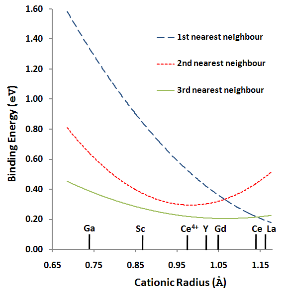
A similar study was recently done by Wei et al.[70] and the relevant part of their results is summarised in Fig. 10.
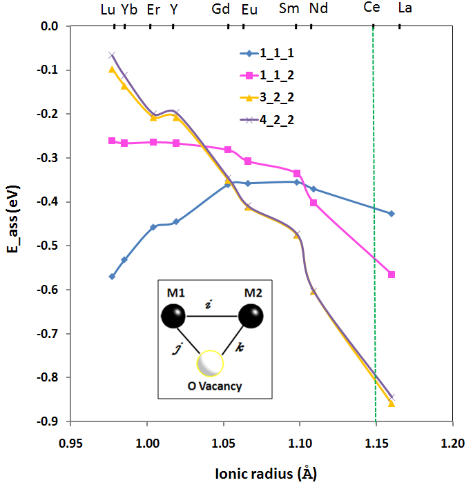
The results of Fig. 10 are for the composition Ce30M2O63 which for M=Ce3+ is the supercell most often used in DFT studies [26, 15, 16, 19, 18]. We have indicated in the figure where results of Ce2O3 are expected to lie based on the ionic radius of Ce3+. The results of Wei et al. [70] can thus be understood as corroborating those of Minervini et al. [68]. From atomistic simulations, Pryde et al. found that the binding energy for a vacancy cluster with two Ce3+ ions in the first coordination shell was significantly less favourable than those with polarons in the second coordination shell ( compared to )[73]. They also found that the defect energetics of clusters involving In3+ ions were qualitatively similar to those for the Ce3+ ions. The results of Pryde et al. on small polaron geometries are consistent with the BVM but contradict the standard picture. Similar results were obtained for doped ZrO2 by DFT methods [74]. We, however, note that in contrast to these results, Deguchi et al. [75] concluded from their extended x-ray absorption fine structure (EXAFS) results that the dopant ions preferred to be in the first coordination shell with respect to the O vacancy.
The higher binding energies for defect associates in which the dopant ions are in the second coordination shell have been explained in the following way [73, 68]: (i) the Coulomb interaction between the and M charged defects which favours the first coordination shell for the dopant ions, (ii) lattice relaxation which primarily has to do with the relaxation of the Ce4+ with respect to the and M charged defects around it. Because of its large positive charge, the Ce4+ ion prefers to relax away from the site towards the M site. This mode of relaxation is not possible if the M ion is a nearest neighbour to the site. Thus, this mode of lattice relaxation always favours the second nearest neighbour site for the dopant ion and (iii) a component of lattice relaxation driven by ion-size effects which favour the nearest neighbour position for small dopants. This is because the small ions prefer lower coordination. For M=Ce3+, effect (ii) is the most dominant and an energy gain of has been reported [68] which explains why the second coordination shell is preferred for these ions. Although we have not discussed the situation for high dopant concentrations where the neutral trimer is expected to dominate, Minervini et al have shown that the behaviour of these more complex systems is qualitatively similar to that of the defect cluster [68].
We note that the atomistic models use the generalized Mott-Littleton method [76] which assumes an ionic description of the crystal lattice and the shell model for the ionic polarizabilities of the ions [77]. It is possible that the assumption of an ionic crystal for CeO2 might not be consistent with the results of bond valence calculations. Also, the models do not include vacancy-vacancy interactions which might be important at high vacancy concentrations as reported recently by Pietrucci et al. [78].
Additional data are needed for a comprehensive comparison with bond valence results. Ideally, one would also like curves of the binding energy as a function of the dopant concentration. The dopant of interest is Ce2O3 and since the reduced phases of ceria considered in this paper are Ce7O12 (CeOCe2O3), Ce11O20 (CeOCe2O3) and Ce6O11 (CeOCe2O3) the mole fraction of the dopant will need to cover the range to . These are well within the capabilities of atomistic modelling. The range could be extended to lower concentrations using the supercell typical of DFT calculations and also in Fig. 10. This classic case is interesting as it will provide an opportunity to compare the results from ab initio electronic structure calculations with those from atomistic modelling.
5 Conclusion
For slightly reduced ceria, the charge distribution obtained from the BVM is consistent with the description of the electronic conductivity by the SPM. For the CeO2-x phases in the neighbourhood of , we anticipate low temperature metallic conductivity or the highest low temperature electronic conductivity of all the reduced ceria phases. This conclusion relies on the estimation of electron hopping amplitudes from Harrison’s method of universal parameters. The detection of this metallic conductivity will discriminate between the standard picture and the BVM desriptions of charge distribution in CeO2-x phases. We have also considered the compatibility of the BVM charge distribution and the atomistic models used to describe ionic conductivity in these phases. We found that the atomistic models and the BVM give a consistent picture of the location of the charge. However, the data are quite limited and it is thus not possible to make a comprehensive assessment.
6 Acknowledgements
We are grateful to Prof. C. Stampfl at the University of Sydney for introducing us to the field of cerium oxides. One of us (E. S) is grateful to the Australian Commonwealth Government Department of Science Education and Training for the award of the International Postgraduate Research Scholarship (IPRS) and to the University of Queensland for the University of Queensland International Postgraduate Research Scholarship (UQIPRS). E. S is also grateful for the School of Mathematics and Physics Postgraduate Travel Scholarship and the Australian Research Council Nanotechnology Network (ARCNN). This work was also supported by the Australian Research Council.
References
- [1] E. Shoko, M. F. Smith, R. H. McKenzie, Mixed valency in cerium oxide crystallographic phases: Valence of different cerium sites by the bond valence method, Phys. Rev. B 79 (2009) 134108.
- [2] E. Shoko, M. F. Smith, R. H. McKenzie, Charge Distribution Near Oxygen Vacancies in Cerium Oxides, arXiv:0907.1320v2 [cond-mat.mtrl-sci].
- [3] S. C. Singhal, K. Kendall (Eds.), High-temperature Solid Oxide Fuel Cells: Fundamentals, Design and Applications, Elsevier Advanced Technology, UK, 2003.
- [4] H. Inaba, H. Tagawa, Ceria-based solid electrolytes, Solid State Ionics 83 (1-2) (1996) 1 – 16. doi:DOI: 10.1016/0167-2738(95)00229-4.
- [5] B. C. H. Steele, Appraisal of Ce1-yGdyO2-y/2 electrolytes for IT-SOFC operation at C, Solid State Ionics 129 (1-4) (2000) 95 – 110. doi:DOI: 10.1016/S0167-2738(99)00319-7.
- [6] V. V. Kharton, F. M. Figueiredo, L. Navarro, E. N. Naumovich, A. V. Kovalevsky, A. A. Yaremchenko, A. P. Viskup, A. Carneiro, F. M. B. Marques, J. R. Frade, Ceria-based materials for solid oxide fuel cells, J. Mater. Sci. 36 (2001) 1105–1117.
- [7] D.-E. Zhang, X.-J. Zhang, X.-M. Ni, J.-M. Song, H.-G. Zheng, Optical and electrochemical properties of CeO2 spindles, ChemPhysChem 7 (12) (2006) 2468–2470.
- [8] A. Trovarelli (Ed.), Catalysis by Ceria and Related Materials, Imperial College Press, London, 2002.
- [9] J. H. Blank, J. Beckers, P. F. Collignon, G. Rothenberg, Redox kinetics of ceria-based mixed oxides in selective hydrogen combustion, ChemPhysChem 8 (17) (2007) 2490–2497.
- [10] H.-T. Chen, Y. M. Choi, M. Liu, M. C. Lin, A theoretical study of surface reduction mechanisms of CeO2(111) and (110) by H2, ChemPhysChem 8 (6) (2007) 849–855.
- [11] L. Mo, X. Zheng, C.-T. Yeh, A novel CeO2/ZnO catalyst for hydrogen production from the partial oxidation of methanol, ChemPhysChem 6 (8) (2005) 1470–1472.
- [12] D. J. Fray, Solid-state gas sensors, in: K. H. J. Buschow, R. W. Cahn, M. C. Flemings, B. I. (print), E. J. Kramer, S. Mahajan, , P. V. (updates) (Eds.), Encyclopedia of Materials: Science and Technology, Elsevier, Oxford, 2001, pp. 8726 – 8730.
- [13] P. Jasinski, T. Suzuki, H. U. Anderson, Nanocrystalline undoped ceria oxygen sensor, Sens. Actuators, B 95 (1-3) (2003) 73 – 77.
- [14] R. L. Martin, Structural theory for non-stoichiometry. part 1. defect fluorite-type structures: Lanthanoid oxides MOx with , J. Chem. Soc., Dalton Trans. (1974) 1335.
- [15] N. V. Skorodumova, S. I. Simak, B. I. Lundqvist, I. A. Abrikosov, B. Johansson, Quantum origin of the oxygen storage capability of ceria, Phys. Rev. Lett. 89 (2002) 166601.
- [16] S. Fabris, S. de Gironcoli, S. Baroni, G. Vicario, G. Balducci, Taming multiple valency with density functionals: A case study of defective ceria, Phys. Rev. B 71 (2005) 041102.
- [17] J. L. F. Da Silva, M. V. Ganduglia-Pirovano, J. Sauer, V. Bayer, G. Kresse, Hybrid functionals applied to rare-earth oxides: The example of ceria, Phys. Rev. B 75 (2007) 045121.
- [18] D. A. Andersson, S. I. Simak, B. Johansson, I. A. Abrikosov, N. V. Skorodumova, Modelling of CeO2, Ce2O3, and CeO2-x in the LDA+ formalism, Phys. Rev. B 75 (2007) 035109.
- [19] C. W. M. Castleton, J. Kullgren, K. Hermansson, Tuning LDA+ for electron localization and structure at oxygen vacancies in ceria, J. Chem. Phys. 127 (2007) 244704.
- [20] M. V. Ganduglia-Pirovano, J. L. F. D. Silva, J. Sauer, Density-functional calculations of the structure of near-surface oxygen vacancies and electron localization on CeO2(111), Phys. Rev. Lett. 102 (2) (2009) 026101.
- [21] H.-Y. Li, H.-F. Wang, X.-Q. Gong, Y.-L. Guo, Y. Guo, G. Lu, P. Hu, Multiple configurations of the two excess electrons on defective CeO2(111): Origin and implications, Phys. Rev. B 79 (19) (2009) 193401.
- [22] A. M. Burow, M. Sierka, J. Döbler, J. Sauer, Point defects in CaF2 and CeO2 investigated by the periodic electrostatic embedded cluster method, J. Chem. Phys. 130 (17) (2009) 174710.
- [23] H. Jiang, R. I. Gomez-Abal, P. Rinke, M. Scheffler, Localized and Itinerant States in Lanthanide Oxides United by GW @ LDA+U, Phys. Rev. Lett. 102 (2009) 126403.
- [24] E. Wuilloud, B. Delley, W.-D. Schneider, Y. Baer, Spectroscopic evidence for localized and extended -symmetry states in CeO2, Phys. Rev. B 53 (1984) 202–205.
- [25] P. J. Hay, R. L. Martin, J. Uddin, G. E. Scuseria, Theoretical study of CeO2 and Ce2O3 using a screened hybrid functional, J. Chem. Phys. 125 (2006) 034712.
- [26] N. V. Skorodumova, R. Ahuja, S. I. Simak, I. A. Abrikosov, B. Johansson, B. I. Lundqvist, Electronic, bonding and optical properties of CeO2 and Ce2O3 from first principles, Phys. Rev. B 64 (2001) 115108.
- [27] E. Shoko, Strong Electronic Correlations in Cerium Oxides, Ph.D. thesis, University of Queensland (2009).
- [28] T. Nakano, A. Kotani, J. C. Parlebas, Theory of XPS and BIS spectra in Ce2O3 and CeO2, J. Phys. Soc. Jpn. 56 (6) (1987) 2201–2210.
- [29] H. L. Tuller, A. S. Norwick, Small polaron electron transport in reduced CeO2 single crystals, J. Phys. Chem. Solids 38 (8) (1977) 859–867.
- [30] T. Holstein, Studies of Polaron Motion. Part II. The “Small” Polaron, Ann. Physics 8 (1959) 343–389.
- [31] D. Emin, T. Holstein, Studies of Polaron Motion. Part IV. Adiabatic Theory of the Hall Effect, Ann. Physics 53 (1969) 439–520.
- [32] R. Marcus, N. Sutin, Electron transfers in chemistry and biology, Biochim. Biophys. Acta. 811 (1985) 265.
- [33] J. R. Bolton, M. D. Archer, Electron Transfer in Inorganic, Organic and Biological Systems, American Chemical Society, 1991, Ch. 2, pp. 7–23.
- [34] J. B. Goodenough, Review Lecture: Fast ionic conduction in solids, Proc. R. Soc. London, Ser. A 393 (1984) 215–234.
- [35] M. Morgensen, N. M. Sammes, G. A. Tompsett, Physical, chemical and electrochemical properties of pure and doped ceria, Solid State Ionics 129 (2000) 63–94.
- [36] H. Mehrer, Diffusion in Solids: Fundamentals, Methods, Materials, Diffusion-controlled Processes, Springer, 2007.
- [37] J. B. Goodenough, Oxide-Ion Electrolytes, Annu. Rev. Mater. Sci. 33 (2003) 91–128.
- [38] H. Mehrer, Diffusion in Solids: Fundamentals, Methods, Materials, Diffusion-controlled Processes, Springer, 2007.
- [39] P. Heitjans, J. Krger (Eds.), Diffusion in Condensed Matter. Methods, Materials, Models, Springer-Verlag, 2005.
- [40] P. Shewmon, Diffusion in Solids, Minerals, Metals & Materials Society, 1989.
- [41] G. Mahan, Many-Particle Physics, Kluwer Academic/Plenum Publishers, 2000.
- [42] V. Butler, C. Catlow, B. Fender, J. Harding, Dopant ion radius and ionic conductivity in cerium dioxide, Solid State Ionics 8 (2) (1983) 109 – 113.
- [43] K. Huang, M. Feng, J. B. Goodenough, Synthesis and Electrical Properties of Dense Ce0.9Gd0.1O1.95 Ceramics, J. Am. Ceram. Soc. 81 (1998) 357 62.
- [44] K. Fuda, K. Kishio, S. Yamauchi, K. Fueki, Y. Onoda, 17O NMR study of Y2O3-doped CeO2, J. Phys. Chem. Solids 45 (11-12) (1984) 1253 – 1257.
- [45] K. Fuda, K. Kishio, S. Yamauchi, K. Fueki, Study on vacancy motion in Y2O3-doped CeO2 by 17O NMR technique, J. Phys. Chem. Solids 46 (10) (1985) 1141 – 1146.
- [46] R. N. Blumenthal, R. L. Hofmaier, The Temperature and Compositional Dependence of the Electrical Conductivity of Non-stoichiometric CeO2-x, J. Electrochem. Soc. 121 (1) (1974) 126.
- [47] D. Y. Wang, D. Park, J. Griffith, A. Nowick, Oxygen-ion conductivity and defect interactions in yttria-doped ceria, Solid State Ionics 2 (2) (1981) 95 – 105.
- [48] W. Lai, S. M. Haile, Impedance spectroscopy as a tool for chemical and electrochemical analysis of mixed conductors: A case study of ceria, J. Am. Ceram. Soc. 88 (2005) 2979–2997.
- [49] S. R. Wang, T. Kobayashi, M. Dokiya, T. Hashimoto, Electrical and Ionic Conductivity of Gd-Dope Ceria, J. Electrochem. Soc. 147 (2000) 3606 – 3609.
- [50] M. B. Salamon, M. Jaime, Manganites: Structure and transport, Rev. Mod. Phys. 73 (2004) 583.
- [51] M. F. Hundley, J. J. Neumeier, Thermoelectric power of La1-xCaxMnO3+δ: Inadequacy of the nominal Mn3+/4+ valence approach, Phys. Rev. B 55 (1997) 11511.
- [52] R. R. Heikes, J. R. W. Ure, Thermoelectricity: Science and Engineering, Interscience Publishers, 1961.
- [53] P. M. Chaikin, G. Beni, Thermopower in the correlated hopping regime, Phys. Rev. B 13 (2) (1976) 647–651. doi:10.1103/PhysRevB.13.647.
- [54] W. A. Harrison, Elementary Electronic Structure, World Scientific, 2004.
- [55] Z. C. Kang, L. Eyring, The structural basis of the fluorite-related rare earth higher oxides, Aust. J. Chem. 49 (1997) 981–996.
- [56] W. A. Harrison, G. K. Straub, Electronic structure and properties of d- and f-shell-metal compounds, Phys. Rev. B 36 (5) (1987) 2695–2706. doi:10.1103/PhysRevB.36.2695.
- [57] H. M. McConnell, Intramolecular charge transfer in aromatic free radicals, J. Chem. Phys. 35 (2) (1961) 508–515.
- [58] G. V. S. Rao, S. Ramdas, P. N. Mehrotra, C. N. R. Rao, Electrical transport in rare-earth oxides, J. Solid State Chem. 2 (3) (1970) 377 – 384.
- [59] A. Trovarelli, Catalysis by Ceria and Related Materials, Imperial College Press, 2002.
- [60] H. Yokokawa, T. Horita, N. Sakai, K. Yamaji, M. Brito, Y.-P. Xiong, H. Kishimoto, Ceria: Relation among thermodynamic, electronic hole and proton properties, Solid State Ionics 177 (19-25) (2006) 1705 – 1714.
- [61] S. Omar, E. D. Wachsman, J. C. Nino, A co-doping approach towards enhanced ionic conductivity in fluorite-based electrolytes, Solid State Ionics 177 (35-36) (2006) 3199 – 3203.
- [62] D. A. Andersson, S. I. Simak, N. V. Skorodumova, I. A. Abrikosov, B. Johansson, Optimization of ionic conductivity in doped ceria, Proc. Natl. Acad. Sci. U.S.A 103 (2006) 3518–3521.
- [63] S. Omar, E. D. Wachsman, J. C. Nino, Higher conductivity Sm3+ and Nd3+ co-doped ceria-based electrolyte materials, Solid State Ionics 178 (37-38) (2008) 1890 – 1897.
- [64] D. Yan, X. Liu, D. Xu, C. Zhu, W. Ma, J. Niu, Y. Liu, W. Su, Effect of Tb co-dopant on the electrical conductivity of Sm-doped ceria electrolyte, Solid State Ionics 179 (21-26) (2008) 995 – 999.
- [65] J. Kilner, R. Brook, A study of oxygen ion conductivity in doped non-stoichiometric oxides, Solid State Ionics 6 (3) (1982) 237 – 252.
- [66] P. Kofstad, Defects and transport properties of metal oxides, Oxid. Met. 44 (1995) 3.
- [67] M. Mogensen, N. M. Sammes, G. A. Tompsett, Physical, chemical and electrochemical properties of pure and doped ceria, Solid State Ionics 129 (2000) 63–94.
- [68] L. Minervini, M. O. Zacate, R. W. Grimes, Defect cluster formation in M2O3-doped CeO2, Solid State Ionics 116 (3-4) (1999) 339 – 349.
- [69] F. Ye, T. Mori, D. R. Ou, A. N. Cormack, R. J. Lewis, J. Drennan, Simulation of ordering in large defect clusters in gadolinium-doped ceria, Solid State Ionics 179 (35-36) (2008) 1962 – 1967.
- [70] X. Wei, W. Pan, L. Cheng, B. Li, Atomistic calculation of association energy in doped ceria, Solid State Ionics 180 (1) (2009) 13 – 17.
- [71] J. Faber, C. Geoffroy, A. Roux, A. Sylvestre, P. Abelard, A systematic investigation of the dc electrical conductivity of rare-earth doped ceria, Applied Physics A 49 (1989) 225–232.
- [72] R. Gerhardt-Anderson, A. Nowick, Ionic conductivity of CeO2 with trivalent dopants of different ionic radii, Solid State Ionics 5 (1981) 547 – 550.
- [73] A. K. A. Pryde, S. Vyas, R. W. Grimes, Cadmium and indium defects in ceria and their interaction with oxygen vacancies and small polarons, Phys. Rev. B 52 (1995) 13214–13222.
- [74] A. Bogicevic, C. Wolverton, Nature and strength of defect interactions in cubic stabilized zirconia, Phys. Rev. B 67 (2003) 024106.
- [75] H. Deguchi, H. Yoshida, T. Inagaki, M. Horiuchi, Exafs study of doped ceria using multiple data set fit, Solid State Ionics 176 (23-24) (2005) 1817 – 1825.
- [76] N. F. Mott, M. J. Littleton, Conduction in polar crystals. I. electrolytic conduction in solid salts, Trans. Faraday Soc. 34 (1938) 485–499.
- [77] B. G. Dick, Jr., A. W. Overhauser, Theory of the dielectric constants of alkali halide crystals, Phys. Rev. 112 (1958) 90–103.
- [78] F. Pietrucci, M. Bernasconi, A. Laio, M. Parrinello, Vacancy-vacancy interaction and oxygen diffusion in stabilized cubic ZrO2 from first principles, Phys. Rev. B 78 (2008) 094301.
7 Graphic Abstract
Is low temperature metallic conductivity possible in Ce7O12? We argue that since the distribution of the excess charge in this crystal can be described by a simple model of a network of equilateral triangles each at filling, band conductivity may be expected.