Diamond Prototypes for the ATLAS SLHC Pixel Detector
Abstract
Vertex detectors at future hadron colliders will need to cope with large particle fluences. Diamond is a particularly radiation hard material and exhibits further properties that makes it an attractive material for such detectors. Within the RD42 collaboration several chemical vapor deposition diamond samples are being studied in the form of strip and pixel detectors. While the quality of the poly-crystalline diamond samples is constantly increasing and the feasibility of producing wafers has been demonstrated, recently a single-crystal diamond pixel detector has been assembled and characterized in a 100 GeV particle beam at CERN. Results on performance, detection efficiency, spatial resolution and charge collection are reported here together with the latest radiation damage studies.
keywords:
vertex detectors, radiation hard sensors, LHC upgrade, ATLAS pixel detector1 Introduction
While the Large Hadron Collider is scheduled to start collecting data this year, the design luminosity of the planned Super Large Hadron Collider (SLHC) of cm-2s-1 poses a serious challenge for future vertex detectors close to the interaction region, in particular due to the harsh radiation environment. In SLHC scenarios the total expected fluence at a radius of about 5cm will exceed particles/cm2. A number of studies are currently being performed to find solutions for detectors that can operate in such environments. Chemical Vapor Deposition diamond, in either single-crystal (scCVD) or polycrystalline (pCVD) form, is one material which is being considered for such detectors. Besides being radiation tolerant, diamond is also an attractive material, since it is an excellent thermal conductor and it exhibits no leakage current, fast collection times and a small input capacitance.
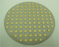
Recently pCVD diamond material has become available in the form of wafers. Figure 1 shows two such diamond wafers with as-grown collection distances of 315m and 310m respectively, produced by Element Six [1]. The collection distance is a measure of the quality of material and routinely exceeds 300m.

After characterizing four full wafers, all indications are that Element Six can reproducible grow and process high-quality detector-grade CVD diamond material. Advances in the production of scCVD diamonds have lead to the production of sensors with sizes larger than 1cm2 and thicknesses of up to 700m. The production process is still in its development and the sensors often come in irregular shapes. scCVD detector material is superior in terms of charge collection and homogeneity than poly-crystalline diamond sensors.
Several diamond pixel detectors have been constructed within the RD42 collaboration, developing and characterizing detectors, in cooperation with the Fraunhofer Institute for Reliability and Microintegration (IZM) [2], performing fine-pitch flip-chip bump bonding. Single-chip devices and also multi-chip module detectors have been assembled and tested in particle beams. Testbeam results for a scCVD pixel detector [3] and a full module pCVD pixel detector [4] are presented in this paper, together with radiation tolerance studies [5].
2 Diamond pixel detectors
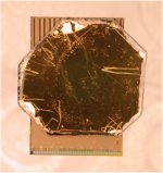
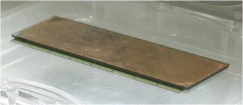
Two diamond pixel detectors have been assembled with standard ATLAS pixel electronics, calibrated in the laboratory and characterized in high-energy particle beams. For assembly, both sides are metallised with Ti/W. One side is segmented into a m2 pixel pattern to match the pattern of the ATLAS pixel front-end chip (FE-I3). Solder (PbSn) bumping and flip-chipping technology at IZM has been employed to mate both parts. Figure 2 shows the two assemblies, a single-chip detector, with an irregularly shaped m thick single-crystal diamond sensor (left) and a m thick full-size, m2 polycrystalline module with 16 front-end chips (right).
The ATLAS pixel electronics provides zero suppression in the readout with a typical threshold level of 3000-4000 electrons and a noise of 160 electrons when used with silicon detectors. As diamond sensors are basically free of leakage currents and have lower input capacitance, the sensor was operated at thresholds of about 1700 electrons with a noise level of about 130 electrons, as determined from fitting the threshold curves of the pixels (S-curves). Analog information is obtained via the in-pixel measurement of time-over-threshold (ToT) with an approximate resolution of 8 bit. The ToT calibration is obtained for every pixel individually, by fitting the ToT response to input pulses injected over a capacitance of 41.4fF.
3 Testbeam performance
The pCVD module has been tested in a 6 GeV electron beam at DESY. The measurements were affected by multiple scattering as reported in [4]. With a bias voltage of 800V a noise of 130 electrons at a threshold of electrons were measured. More than of the electronics channels were operational.
The scCVD single-chip module was tested in a 100 GeV pion test beam at CERN, using the Bonn-ATLAS telescope [6] as a reference for tracking and efficiency measurements. It consists of double-sided silicon microstrip detectors with m pitch. Only tracks with a single hit in each telescope plane are selected. The extrapolated spatial uncertainty at the device under test (DUT) is m.
Unlike in silicon the electric field inside good scCVD diamond is fairly uniform and thus the spatial response of the detector was uniform for bias voltages larger than 0.25 V/m. Due to the faster charge collection smaller cluster sizes are observed at increasing bias voltages. The measured most probable charge value (MPV) in the sensor at 400 V is 13.1 ke compatible with the expected value using the ToT charge calibration outlined in [3]. The measured MPV increases with the applied bias voltage and saturate above 100 V, indicating that the charge collection is complete above these values. For full charge collection single and double hit clusters have roughly equal sharing. The overall efficiency to find a hit near a track point extrapolated on the plane of the DUT is found to be .
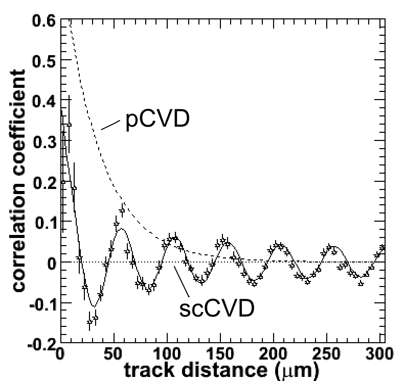
Charge collection and space point reconstruction in pCVD are affected by the grain structure and the trapping of electric charges at their boundaries which may cause horizontal polarization fields. In [7] it was observed that the distribution of residuals across the sensor is not statistically distributed but exhibits regions with systematically positive or negative residuals on a scale smaller than m. To quantify this apparent clustering, the linear correlation coefficient between the residuals of all track pairs has been determined. Since each selected event has exactly one reconstructed track, pairs are formed considering tracks of two different events. The average correlation coefficients are determined in bins of the distance between the two tracks of a pair. An empirical function, a sum of a sinusoidal modulation with the periodicity of the pixel pitch with a falling exponential that accounts for the residual shifts introduced by the grain structure, was found to provide a good description of the data. In [7] the data for a low-quality pCVD diamond were fit, resulting in a correlation length (the decay factor in the exponential) of m. Here, we repeat this measurement for the scCVD single-chip detector. Since there are no grain boundaries the device exhibits optimal charge collection and a correlation length compatible with m is observed [3], indicating the absence of horizontal polarization fields. This is illustrated in Figure 3.
The spatial resolution is shown in Figure 4, where the difference between the track position predicted by the telescope on the plane of the DUT (the scCVD sensor) and the reconstructed hit of the DUT device is shown for both directions of the pixel.
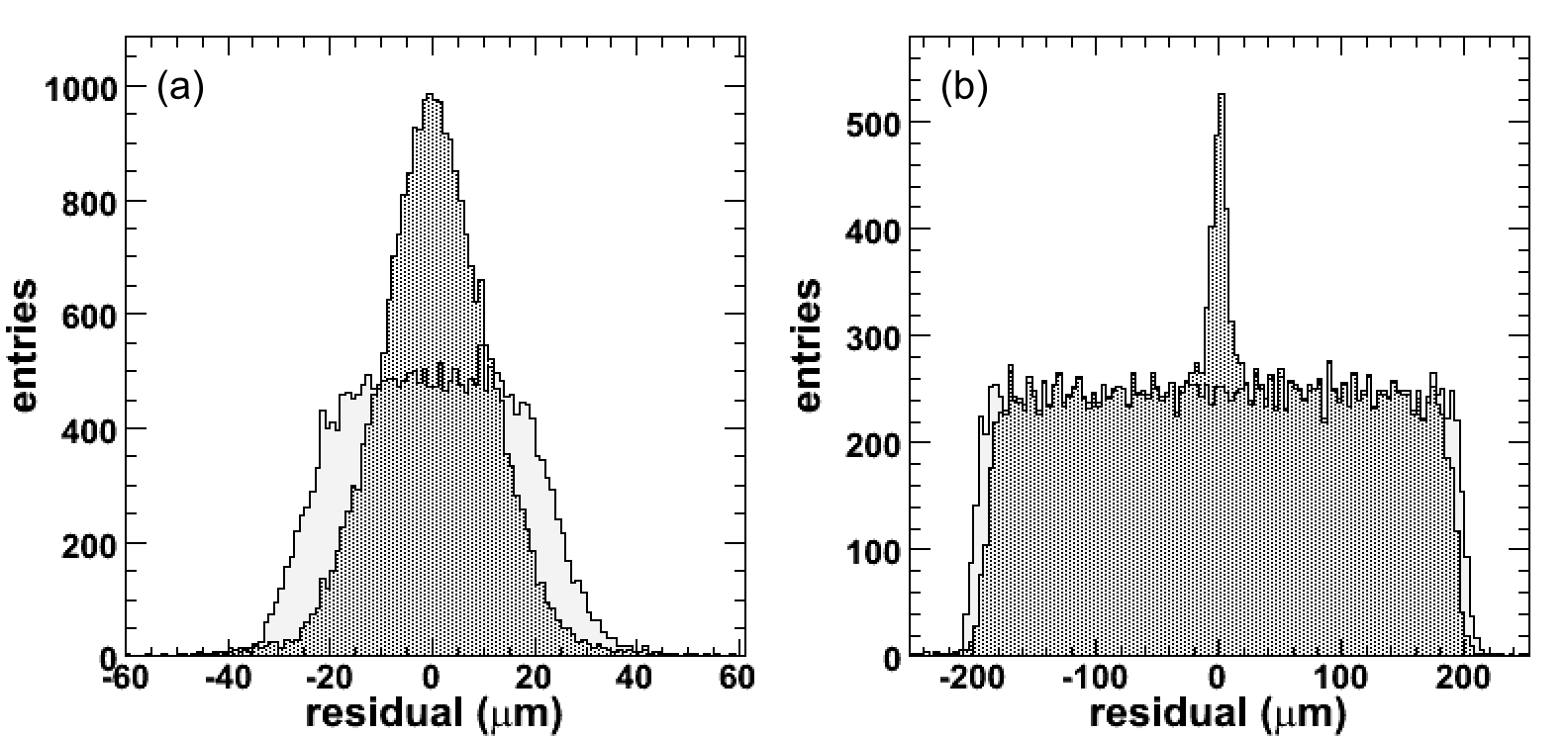
For the hit reconstruction first only the digital information is used (light gray distribution), i.e. the pixel with the largest charge signal above threshold collected in a cone around the extrapolated track position is taken as the hit pixel and its center is assumed to be the reconstructed position. The expected digital resolutions of pixel pitch divided by in both directions, i.e. 14.4 m and 115.5 m, respectively, folded by the resolution of the track extrapolation of about 5 m, is observed. Position reconstruction which exploits the analog information available via the ToT readout is done by using the -algorithm [8]. The corresponding residual distribution is shown by the dark histograms in Figure 4. It shows a pronounced peak with good resolution for clusters with two pixel hits, for which the -algorithm improves the resolution substantially. In the short pixel direction where the fraction of two hit clusters is about 40% the intrinsic resolution of the device, after quadratically subtracting the telescope extrapolation error of 5m, becomes ()m for a bias voltage of 200V. The error quoted is obtained from the fit to the residual distribution. Repeating the analysis on several data samples indicate an additional systematic uncertainty in the order of 0.5m. In the direction of the long pixel dimension, the resolution for events with two-hit clusters (10%) is an order of magnitude better than for events with single hit clusters. The space resolution depends on the bias voltage. The charge collection efficiency and hence the total collected charge are field dependent until full charge collection is obtained. Also the sharing of charge between pixels due to diffusion depends on the field inside the sensor. The measured resolution shows an optimum between both effects at bias voltages of 200V [3] for this device.
4 Radiation Hardness
The RD42 irradiation program consists of testing each sample prepared as a detector in a CERN test beam before and after irradiation. Previously, diamond samples were irradiated with reactor neutrons and charged pions. Most recently we irradiated the highest quality polycrystalline CVD diamond with 24 GeV protons from CERN PS to a fluence of p/cm2.
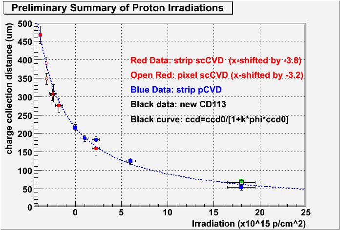
Figure 5 shows the signals observed in various pCVD and scCVD diamond sensors after a range of irradiations. The scCVD diamond is expected to be representative of the next generation high quality polycrystalline material. A single damage curve given by the equation ccd-1 = ccd, with ccd0 the initial collection distance and the damage constant can accommodate for the different measurements shown, with one universal constant . In particular, also the measurements on the scCVD fall on the same curve if shifted by p/cm2. The interpretation is that, owing to the intrinsic crystallite structure, the unirradiated pCVD material behaves as effectively having the same number of trapping centers as the scCVD material after a dose of p/cm2. After ten years of SLHC running typical fluences of p/cm2 are anticipated for vertex detectors at 4cm. From Figure 5 we see that diamond sensors still retain an average signal of 2500 electrons after such fluences [9].
References
- [1] Element Six Ltd., King’s Ride Park, Ascot, Berkshire, SL5 8BP, United Kingdom.
- [2] Fraunhofer Institut für Mikrointegration, Gustav-Meyer-Allee 25, Berlin, Germany.
- [3] M. Mathes et al., 2008 JINST 3 P12002.
- [4] M. Mathes, Ph.D thesis, urn:nbn:de:hbz:5N-16430.
- [5] M. Barbero et al. (RD42 Collaboration), CERN/LHCC 2008-005, LHCC-RD-016.
- [6] J. Treis et al.,Nucl. Instr. and Meth. A 490 (2002) 112.
- [7] T. Lari et al., Nucl. Instr. and Meth. A 537 (2005) 581.
- [8] E. Belau et al.,Nucl. Instr. and Meth. A 214 (1983) 253.
- [9] W. Trischuk for the RD42 collaboration, Proc. of the 34th ICHEP, to appear.