Solving dielectric and plasmonic waveguide dispersion relations on a pocket calculator
Rohan D. Kekatpure, Aaron C. Hryciw, Edward S. Barnard, and
Mark L. Brongersma
Geballe Laboratory for Advanced Materials, Stanford University, Stanford, CA, 94305
brongersma@stanford.edu
Abstract
We present a robust iterative technique for solving complex transcendental dispersion equations routinely encountered in integrated optics. Our method especially befits the multilayer dielectric and plasmonic waveguides forming the basis structures for a host of contemporary nanophotonic devices. The solution algorithm ports seamlessly from the real to the complex domain—i.e., no extra complexity results when dealing with leaky structures or those with material/metal loss. Unlike several existing numerical approaches, our algorithm exhibits markedly-reduced sensitivity to the initial guess and allows for straightforward implementation on a pocket calculator.
OCIS codes: 000.0360,000.4430,240.6680,250.5403,240.0240
References and links
- [1] M. L. Brongersma and P. G. Kik, eds., Surface Plasmon Nanophotonics, vol. 131 of Springer series in optical sciences (Springer, 2007).
- [2] R. Zia, J. A. Schuller, and M. L. Brongersma, “Plasmonics: The next chip-scale technology,” Materials Today 9, 20–27 (2006).
- [3] R. A. Pala, J. S. White, E. S. Barnard, J. Liu, and M. L. Brongersma, “Design of plasmonic thin-film solar cells with broadband absorption enhancements,” Advanced Materials 21, 1–6 (2009).
- [4] W. H. Press, S. A. Teukolsky, W. J. Vetterling, and B. P. Flannery, Numerical recipes in C++, The art of scientific computing (Cambridge University Press, 2002), 2nd ed.
- [5] A. W. Snyder and J. Love, Optical waveguide theory (Science Paperbacks, 1983).
- [6] J. Takahara, S. Yamagishi, H. Taki, A. Morimoto, and T. Kobayashi, “Guiding of a one-dimensional guiding of a one-dimensional optical beam with nanometer diameter,” Opt. Lett. 22, 475–477 (1997).
- [7] J.-C. Weeber, Y. Lacroute, and A. Dereux, “Optical near-field distributions of surface plasmon waveguide modes,” Phys. Rev. B 68, 115401 (2003).
- [8] R. Zia, A. Chandran, and M. L. Brongersma, “Dielectric waveguide model for guided surface polaritons,” Opt. Lett. 30, 1473–1475 (2005).
- [9] R. Zia, J. A. Schuller, and M. L. Brongersma, “Near-field characterization of guided polariton propagation and cutoff in surface plasmon waveguides,” Physical Review B (Condensed Matter and Materials Physics) 74, 165415 (2006).
- [10] R. Zia, M. D. Selker, and M. L. Brongersma, “Leaky and bound modes of surface plasmon waveguides,” Phys. Rev. B 71, 165431 (2005).
- [11] G. Veronis and S. Fan, “Bends and splitters in metal-dielectric-metal subwavelength plasmonic waveguides,” Applied Physics Letters 87, 131102 (2005).
- [12] G. Veronis and S. Fan, “Guided subwavelength plasmonic mode supported by a slot in a thin metal film,” Opt. Lett. 30, 3359–3361 (2005).
- [13] S. I. Bozhevolnyi, V. S. Volkov, E. Devaux, J.-Y. Laluet, and T. W. Ebbesen, “Channel plasmon subwavelength waveguide components including interferometers and ring resonators,” Nature 440, 508–511 (2006).
- [14] E. Anemogiannis, E. N. Glytsis, and T. K. Gaylord, “Determination of guided and leaky modes in lossless and lossy planar multilayer optical waveguides: reflection pole method and wavevector density method,” Journal of Lightwave Technology 17, 929–941 (1999).
- [15] R. Zia, M. D. Selker, P. B. Catrysse, and M. L. Brongersma, “Geometries and materials for subwavelength surface plasmon modes,” J. Opt. Soc. Am. A 21, 2442–2446 (2004).
- [16] S. E. Kocabaş, G. Veronis, D. A. B. Miller, and S. Fan, “Modal analysis and coupling in metal-insulator-metal waveguides,” Phys. Rev. B 79, 035120 (2009).
- [17] J. P. McKelvey, “Simple iterative procedures for solving transcendental equations with the electronic slide rule,” American Journal of Physics 43, 331–334 (1975).
- [18] J. Dugundji and A. Granas, Fixed Point Theory (Springer-Verlag, 2003).
- [19] C. R. Pollock, Fundamentals of Optoelectronics (McGraw-Hill Professional Publishing, 2003).
- [20] J. J. Burke, G. I. Stegeman, and T. Tamir, “Surface-polariton-like waves guided by thin, lossy metal films,” Phys. Rev. B 33, 5186–5201 (1986).
- [21] H. Raether, “Surface plasmons on smooth and rough surfaces and on gratings,” Springer Tracts Mod. Phys. 111, 1–133 (1988).
1 Introduction
With an ever-improving ability to fabricate miniature functional components, the field of nanophotonics is in a phase of explosive growth. Not only are novel phenomena being routinely observed in wavelength- and sub-wavelength-scale components, but these concepts are being rapidly translated into exotic devices for applications ranging from solar energy and information technology, to biology [1, 2, 3]. At the heart of this development is the ability of nanostructures to confine, guide, and scatter light in ways that are not achievable with bulk materials. It follows that understanding and improving the performance of these nanostructures requires a detailed knowledge of the electromagnetic modes they support.
The allowed electromagnetic modes in microphotonic structures are determined by solving Maxwell’s equations for the given geometry. The last step in this procedure is the application of boundary conditions at the interfaces, yielding the dispersion equations which must be solved to obtain the allowed modes. These dispersion equations are in general transcendental and except in a few simple cases, their solutions cannot be expressed in terms of elementary mathematical functions.
When the solutions of the dispersion equations are known to be real, they are usually determined using a graphical search algorithm such as the bisection method [4]. However, in lossy material systems or low index-contrast asymmetric waveguides, the dispersion equations have complex solutions [5]. This calls for a search in two dimensions (i.e., in the complex plane) and severely limits the effectiveness of graphical algorithms.
Material loss and waveguide leakage are even more commonly encountered in plasmonic waveguides [1]. Due to the growing technological and scientific clout of plasmonic systems [6, 7, 8, 9, 10, 11, 12, 13]various techniques for solving plasmon waveguide dispersion equations are in current use. Examples include the reflection-pole method (RPM) [14, 15], Newton’s method [4], and the argument-principle method [16]. Practical implementation of these methods requires careful programming customized for solving the problem at hand. In the methods that rely on curve-fitting, increasing the accuracy beyond a few decimals is often a challenging task, often requiring one to iterate the procedure manually based on previous results. Additionally, the root-finding algorithms of several commercial mathematical software suites (e.g., Mathematica™) can be very sensitive to initial guesses provided by the user; estimation of this initial guess is especially difficult when the solution is complex.
In this paper, we present an easy-to-implement iterative procedure for solving complex transcendental dispersion equations that is relatively insensitive to initial guess. Our method applies to rectangular multilayer dielectric and plasmonic waveguides which may have either material or leakage loss. We first use a simple numerical example to illustrate the use of this technique and its convergence behavior. We then successively apply the procedure to find modes of dielectric slab waveguides, photonic wire waveguides, and plasmonic waveguides.
Papers in the past have discussed the use of iterative techniques for solving transcendental equations in general [17]. Our aim in this paper is to demonstrate how this method can be applied to automate the design and analysis of waveguide structures of significant contemporary interest.
2 Iterative technique: A simple example
Although the general philosophy of iterative methods is well known, we will use a simple example to introduce our terminology, illustrate the procedure use, and build an intuitive understanding of convergence issues. Suppose we need to solve the equation:
| (1) |
where is a combination of elementary mathematical functions. We reformulate this as an iterative problem by converting Eq. (1) to:
| (2) |
where is obtained by manipulating the parent function . Next, we start with an initial guess and obtain a sequence according to:
| (3) |
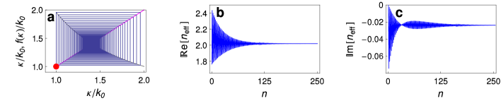
If the sequence defined by Eq. (3) converges, then the limiting value is the solution to Eq. (2). We will illustrate the method by a simple example. Consider the transcendental equation
| (4) |
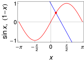
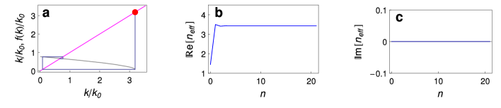
Fig. 1 shows the graphs of the left-hand side (LHS) and right-hand side (RHS) of Eq. (4), which intersect around . To find the root more accurately by the iterative method, we recast the equation in a form similar to Eq. (2) by choosing , setting up an iteration scheme following Eq. (3):
| (5) |
Fig. 2(b) plots the first fifty iterations of Eq. (5) and indicates that the sequence converges to . We compare the 16-decimal agreement between this value and the solution computed by Mathematica™’s FindRoot function. Fig. 2(c) shows the LHS and RHS of the iteration scheme in Eq. (5) and Fig. 2(a) shows how the procedure converges to the intersection point of the two curves, starting from the initial guess. Making an initial guess corresponds to choosing a point on the curve shown by the red curve in Fig. 2(a). This point is indicated in Fig. 2(a) by the red dot. The vertical lines in the spiral represent computation of for the chosen and the horizontal lines represent re-substitution of by for the next iteration.
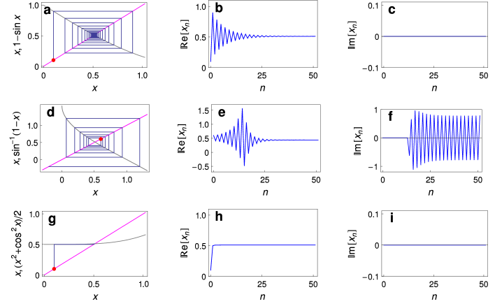
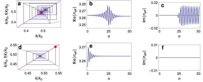
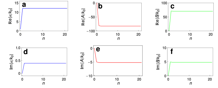
Before we proceed to apply the iterative technique to practical waveguide problems, it is useful to gain an intuitive understanding of how the above scheme converges to the solution. This is important since, for any given , there are usually multiple ways to choose which differ in their convergence behavior. For example, an equally-legitimate way of setting up an iteration scheme for Eq. (4) would be to choose and obtain the sequence according to:
| (6) |
The behavior of successive iterates is shown in Fig. 2(d–f). Regardless of how close the initial guess is to the actual solution, the iterative scheme diverges (spirals away) from the intersection point. Although the real part of the solution appears to converge after about 25 iterations, the overall complex solution does not converge, as seen from the undamped oscillations in the imaginary part of the solution. Thus, this iteration scheme, although derived from the same parent equation, does not converge. This behavior is typical for transcendental equations involving trigonometric functions and is therefore encountered for waveguide problems, as we will show in section 4.2.
On the other hand, convergence of Eq. (4) can be improved considerably by choosing an alternative iterative form as follows. Squaring both sides of Eq. (4) yields:
| (7) |
from which we can obtain yet another sequence of of iterations according to:
| (8) |
Fig. 2(g–i) depict the convergence of succesive iterates of Eq. (8). By comparing Fig. 2(b) with Fig. 2(h) it is apparent that Eq. (8) converges to the solution significantly faster than Eq. (5).
The preceding examples illustrate the crucial importance of choosing appropriate iterative forms. Arriving at such a form necessitates an understanding of the convergence of the iterative scheme. Figure 3 pictorially shows the criterion for convergence of the iterative scheme in Eq. (2). Whether the iteration spirals toward the intersection point (the solution) or away from it is governed by the relative slopes of the intersecting curves. If is steeper than (i.e., if ), the successive computations and re-substitutions spiral away from the intersection and the solution diverges. On the other hand, if rises gently compared to (i.e., if ), then the scheme spirals toward the intersection and the solution converges. For convergent functions, the rate of convergence is governed by the magnitude of . The RHS of Eq. (8) is much flatter () near the solution compared to the RHS of Eq. (5), which results in the latter’s considerably slower convergence. While the preceding justification is not a rigorous proof, it provides a basis for choosing the manipulations required to obtain convergent forms of the practically-useful equations we consider in the forthcoming sections [18].
3 Dispersion equation of a general asymmetric three-layer structure
The design of many integrated photonics systems of practical importance—including both novel plasmonic waveguide architectures as well as conventional dielectric waveguides—can often be reduced to solving for the effective mode index and electromagnetic field distributions in a three-layer planar structure. As such, we focus our analysis on a generalized three-layer slab waveguide, as shown in Fig. 4(a). The central layer is called the core and has a complex relative permittivity . The bottom and top cladding layers are called the substrate (with permittivity ) and cover (with permittivity , respectively.
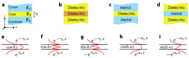
Depending on which materials comprise the three layers, it is possible to classify the most commonly-encountered waveguides into three basic types. The dielectric waveguides, shown in Fig. 4(b), have all three layers made of dielectrics, with . The structures in Figs. 4(c) and (d) are two basic configurations of plasmonic waveguides. The first, shown in Fig. 4(c), consists of an dielectric sandwiched between two (possibly different) metals and is commonly known as a metal-dielectric-metal (MDM) waveguide. The second structure, shown in Fig. 4(d), consists of a metal layer between two (possibly different) dielectrics; it is commonly known as an dielectric-metal-dielectric (DMD) waveguide.
Figures 4(e–i) schematically show the possible modes of a general three-layer slab waveguide. These modes are distinguished according to several criteria: mode number (number of zero-crossings in the field), polarization (transverse electric or transverse magnetic), field symmetry (even or odd), and field profile in the core (sinusoidal or hyperbolic). Of the possible field profiles shown in Fig. 4, the mode shown in (e), having sinusoidal core-field variation with no zero-crossings, is exclusive to dielectric waveguides and is known as the fundamental mode. Modes (h) and (i), having hyperbolic core-field variation, are exclusive to plasmonic waveguides and are known as the gap-plasmon modes. Modes (f) and (g), having sinusoidal core-field variation with zero-crossings, are common to both dielectric and plasmonic waveguides.
This rich variety of modes arises out of the solutions of the dispersion equation written for an asymmetric three-layer slab waveguide. In principle, a single dispersion equation can completely describe all the modes of both dielectric and plasmonic waveguides. However, because the nominally-assumed core-field distributions for the two types are different (sinusoidal for dielectric waveguides and hyperbolic for plasmonic waveguides), we choose to write two separate equations for the two types [19, 20]:
| (9) | |||||
| (10) |
For convenience, we have collected the symbol definitions and their expressions in Table 1. Using these definitions, Eqs. (9) and (10) can be cast explicitly as transcendental equations in a single complex variable or . Furthermore, it is evident that Eq. (9) transforms to Eq. (10) for purely imaginary values of (i.e., ). Having solved for or , the mode’s complex effective index may be calculated using relations in Table 1.
| Symbol | Definition/Expression |
|---|---|
| 1 (for TE), (for TM) | |
| 1 (for TE), (for TM) | |
| , | , |
| , | , |
| , | , |
| , | , |
| , | , |
| , | , |
| , | , |
| (sinusoidal core-fields), | |
| (hyperbolic core-fields) |
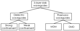
We will now begin the description of the actual iterative solution procedure. We saw in section 1 that the convergence of this technique depends crucially on the iteration function. As a result, the iterative form for determining modes with sinusoidal core-fields [Fig. 4(e–g)] is different from the one needed for determining modes with hyperbolic core-fields [Fig. 4(h–i)]. Therefore, we split our description into two broad categories: dielectric waveguides and plasmonic waveguides. These two categories are further divided depending upon the degree of confinement (strong or weak) for dielectric waveguides, and core/cladding type (MDM or DMD) for plasmonic waveguides. Figure 5 depicts the division of the waveguide modes that we have made for the purposes of describing our iterative solution process. In the forthcoming sections, we will obtain and test rapidly-convergent iterative forms for calculating the mode indices of these four sub-categories of three-layer asymmetric slab waveguides. These useful forms will be boxed for the convenience of the reader.
4 Modes of dielectric waveguides
4.1 Strong-confinement dielectric waveguides
Using the half-angle identity , Eq. (9) can be transformed to:
| (11) |
Inverting the tangent function in Eq. (11) gives us the convergent iterative form for strong-confinement waveguides as:
| (12) |
Here is an integer and the quantities , , , and are related to the iterate through the relationships in Table 1. Although the form of Eq. (12) may seem daunting, we note that it is a general equation which can calculate odd and even modes of both transverse electric (TE) and transverse magnetic (TM) polarizations for asymmetric slab waveguides. All of the functions involved in Eq. (12) are found on scientific calculators and in mathematical software tools. The iterative procedure obviates any need for a graphical search and has an inherent ability to give arbitrary-precision solutions—a feat difficult to achieve using graphical interpolation.
Before embarking on actual computation, we need to specify the parity ( or sign), order (), and the polarization ( and ) of the desired mode. For TE polarization () and even parity ( sign), the effective indices of successive even TE modes may be simply calculated by setting and iterating according to Eq. (12); this yields the TE0, TE2, TE2m modes. For TE polarization with odd parity ( sign), setting yields the TE1, TE3, TE2m-1 modes. Note that for even modes, the mode order begins with , whereas for odd modes, it begins with . The procedure for obtaining TM mode indices is identical, with proper input of as shown in Table 1.
To illustrate the use of the iterative method, we choose a 1--thick silicon-on-insulator (SOI) slab waveguide operating at 1550 nm as a test structure. The refractive indices of the silicon film, oxide substrate, and air cover are assumed to be , and respectively. Using the TE0 mode as an example, Fig. 6 depicts how Eq. (12) converges to the solution. Fig. 6(b) and (c) show the real and imaginary values of the first twenty iterates of Eq. (12). Although the iteration is carried out in terms of , we have chosen to depict the convergence in terms of the effective index since this is a more familiar quantity in waveguide analysis. Fig. 6(a) shows the LHS and RHS of Eq. (12) and how the iterative scheme converges to the solution. Notice that the slope condition mentioned in section 1 is satisfied for this particular case.
To examine the iterative technique in contrast with standard numerical techniques, we solved for the modes of the same structure using Mathematica™.Table 2 compares the two solutions. Mathematica™ calculations were performed by feeding Eq. (11) to the FindRoot function with an initial guess dependent on the mode order, parity, and polarization. To obtain the initial guesses, we plotted the left- and right-hand sides of Eq. (11) and made a manual estimate based on the intersection of the graphs. Given the multiple solutions inherent in Eq. (11), these initial guesses needed to be fairly close to the actual solution for Mathematica™ to return the correct solution. On the other hand, all iterative solutions in Table 1 were initiated with the same initial guess . Moreover, the convergence of the iterative technique is completely insensitive to the exact value of this initial guess: we obtained the same effective indices for initial guesses ranging from to (including complex values). While a precise mathematical characterization of the convergence behavior is outside the scope of our paper, this exercise does suggest the robustness of the iterative technique with respect to the accuracy of the initial guess.
| Mode | Parity | Iterative scheme | Mathematica™ | ||
|---|---|---|---|---|---|
| TE0 | (1,1) | + | 0 | 3.4347458991523551 | 3.4347458991523551 |
| TE1 | (1,1) | - | 1 | 3.2327892969869200 | 3.2327892969869201 |
| TE2 | (1,1) | + | 1 | 2.872310278807719 | 2.872310278807719 |
| TE3 | (1,1) | - | 2 | 2.302024617480549 | 2.302024617480549 |
| TM0 | + | 0 | 3.4165068626393461 | 3.4165068626393461 | |
| TM1 | - | 1 | 3.1541909024008027 | 3.1541909024008027 | |
| TM2 | + | 1 | 2.668932488161409 | 2.668932488161409 | |
| TM3 | - | 2 | 1.865243634178012 | 1.865243634178012 |
4.1.1 Symmetric strong-confinement waveguides
If the relative permittivities of the cover and the substrate are equal, then the structure is called a symmetric waveguide. Since several important photonic device structures employ symmetric waveguides, we now give explicit iterative forms for calculating their mode indices. These iterative forms arise out of the simplifications in Eq. (12) due to the equality of and :
| (13a) | ||||
| (13b) | ||||
We also note that, like Eq. (12), assumes values starting from for even modes and for odd modes.
4.2 Weak-confinement dielectric waveguides
Eq. (12) converges for a very wide range of refractive indices, wavelengths, and waveguide thicknesses which are commonly used in practical integrated photonics designs. It performs poorly, however, when applied to the weak-confinement single-mode waveguide structures routinely fabricated out of III-V (e.g., GaAs/AlGaAs) or organic materials. In the context of multimode waveguides, the strong-confinement formula encounters convergence problems when used to calculate indices of modes near the waveguide cutoff. We highlight this limitation and its remedy through the following example.
Consider a 1--thick air-clad GaAs waveguide on an Al0.1Ga0.9As substrate operating at 1550 nm. The refractive indices of GaAs and Al0.1Ga0.9As are assumed to be and respectively. We attempt to find the fundamental TE mode iteratively by inputting the corresponding parameters to Eq. (12) (, , and sign). Fig. 7(b) and (c) show the behavior of the real and imaginary parts of the calculated effective index for first 50 iterates. The real part of the effective index initially diverges to reach a maximum at iteration number 30 and begins to converge thereafter. Starting from the thirtieth iteration, the imaginary part oscillates between . These oscillations do not damp out even if we increase the number of iterations to . Mathematica™, however, indicates that this structure supports TE0 and TM0 modes with indices of 3.266 and 3.263, respectively. We conclude that the iterative scheme in Eq. (12) fails to converge for this example.
This failure to converge can be understood by examining the behavior of the LHS and RHS of Eq. (12) near the intersection point, as shown in Fig. 7(a). Near the solution, . As a result, the iterates begin to diverge away from the intersection point. In fact, continues to increase away from the intersection, causing a rapidly-increasing divergence. However, at , abruptly becomes , causing the real part of the iteration to converge. This convergence of the real part is misleading, however since the imaginary part shows undamped oscillations. The behavior of the strong confinement formula in this case is similar to the example problem in section 1 illustrated in Fig. 2(d–f).
In summary, the basic cause of the failure of convergence is the breakdown of the slope condition mentioned in section 1. This is remedied by recasting Eq. (9) into a form which satisfies the convergence condition. To this end, we use the identity , rewriting Eq. (9) as:
| (14) |
| Mode | Iterative scheme | Mathematica™ | |
|---|---|---|---|
| TE0 | (1,1) | 3.26599646645606654 | 3.26599646645606654 |
| TM0 | 3.26338400537407312 | 3.26338400537407312 |
The convergent form suitable for weak confinement is obtained by solving for contained in the term on the right hand side of Eq. (14):
| (15) |
where and are related to through the relationships in Table 1. We emphasize that Eq. (15) is a general equation capable of solving for near-cutoff TE and TM modes of odd and even parity in three-layer asymmetric slab waveguides. The choice of or sign in Eq. (15) depends on whether the cutoff occurs at the odd or the even mode. When analyzing a given structure, it is difficult to determine a priori the parity of the cutoff mode. The prescription is therefore to use the strong-confinement formula until it fails to converge, continuing with the weak-confinement formula thereafter. The domain of convergence of the strong- and weak-confinement formulas may be determined rigorously by setting the derivatives of the RHS of Eqs. (12) and (15) equal to 1 and solving for the corresponding value of .
Solving for the mode indices of the previously-considered GaAs/Al0.1Ga0.9As waveguide using Eq. (15) yields the effective indices of the TE0 and TM0 modes in excellent agreement with the Mathematica™ results, as seen from Table 3. The convergence behavior of the effective index is plotted in Fig. 7(d–f). The convergence of Eq. (15) improves as the core–cladding index contrast decreases; similarly, the convergence of Eq. (12) improves for increasing core–cladding index contrast.
4.2.1 Symmetric weak-confinement dielectric waveguides
Similarly to strong-confinement waveguides, having identical cover and substrate indices considerably simplifies the iterative form for weakly-confined slab waveguides, which can be written as:
| …for even modes. | (16a) | ||||
| …for odd modes. | (16b) | ||||
4.3 Extension to photonic wire waveguides
Waveguides in which light is confined in two dimensions and propagates in the third dimension are known as photonic wire (PW) waveguides; optical fibers, as well as ridge, rib, and channel waveguides are examples. Because they offer stronger light confinement compared to slab waveguides, PW waveguides are commonly employed in on-chip optical devices where a small size is essential for achieving several critical device specifications ( e.g., speed, low power, integration density, etc.).
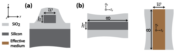
Although the exact field distribution in PW waveguides is best determined by numerical calculations, the effective index method (EIM) is remarkably successful at quickly calculating the mode indices for several common PW waveguide configurations [19]. A knowledge of the effective index suffices for many important design problems. Figure 8 illustrates the two steps in the implementation of EIM. Figure 8(a) shows an idealized silica-clad SOI photonic wire waveguide having a width and thickness . In the first step, we disregard the confinement in the -direction and solve for the effective index . Depending on the polarization of the desired mode, we will need to solve either the TE or TM equation. In the second step, we consider a silica-clad slab waveguide with a core index confined in the -direction. Note that the orientation of the effective waveguide is orthogonal to that in the first step and hence the equation in this step is for the polarization orthogonal to that in the previous step. That is, if the first step uses the TE dispersion equation, then the second step uses the TM equation(and vice versa). The effective index determined in this second step is our final answer for the effective mode index of the original PW waveguide.
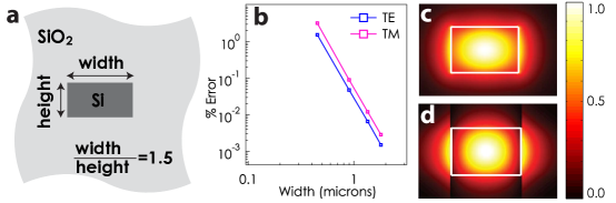
As an example, suppose that we need to determine the effective index of the fundamental -polarized mode of a sub-micron PW waveguide shown in Fig. 9 (a) with and . In the first step, we solve for the TE mode equation for the structure shown in Fig. 8(b). Since SOI waveguide constitutes a strong-confinement system, the first step is readily accomplished by iteration of Eq. (12) for the TE condition (namely, , ). This yields the first effective index as . In the second step, we consider an -confined slab with core-index and iterate Eq. (12) with the fundamental TM mode condition. This yields the effective index of the PW waveguide as .
To test the relative accuracy of the iterative method, we use the finite element method (FEM) to compute the mode index. For the waveguide with the above dimensions, FEM gives . It is evident that even for sub-mircron dimensions, the relative error defined as is only 1.5%. Figure 9(b) shows the variation of the relative error with waveguide dimensions for a fixed width-to-height aspect ratio of 1.5, from which we note the exponential drop in the relative error with increasing waveguide size. The reason for the decrease of accuracy with decreasing size lies in the increased interaction of the electromagnetic fields with the corner regions of the waveguide. By decomposing a two-dimensional mode-solving problem into two one-dimensional problems, we effectively chose to neglect the interaction of the fields with the waveguide corners. This assumption becomes decreasingly accurate with decreasing waveguide size. Figure 9(c) and (d) show the -component of the electric field, calculated using FEM and the iterative method, for the sub-micron waveguide considered above. Note the strong electric field at the waveguide corners in Fig. 9(c) calculated using FEM, and its absence in Fig. 9(d) calculated using the iterative method. In addition to highlighting this difference for small waveguides, this exercise illustrates the well-known fact that while EIM successfully calculates the effective indices, it does not guarantee satisfaction of the boundary conditions. It should therefore not be used to calculate fields for wavelength-sized structures.
In spite of this limitation, the EIM remains an intuitive way of accomplishing designs which rely primarily on the knowledge of mode indices. Examples of such designs include several contemporary device structures such as SOI ring resonators, Bragg gratings, Mach-Zehnder interferometers, and directional couplers. By offering a simple means of solving the slab waveguide dispersion equation, the iterative method greatly enhances the efficacy and implementation speed of EIM.
5 Modes of plasmonic waveguides
The examples in the preceding sections indicate the relative simplicity of the iterative method when applied to dielectric waveguides. However, the true advantage of this technique emerges when dealing with systems having material loss (complex permittivity) or leakage loss (complex propagation constant). The modal indices are complex in both these cases and providing graphical root-finders with a complex initial guess becomes difficult. As such, the self-converging behavior of the iterative algorithm becomes an invaluable asset.
Propagation loss and waveguide leakage arise routinely in sub-wavelength-scale metallic waveguides. Intense research efforts are currently underway in the field of metal-based optics, also known as plasmonics (see, e.g., [1] and references contained therein). Extended metal structures support surface plasmon-polariton (SPP) modes that are electromagnetic waves strongly coupled to collective electron oscillations in the metal. To exploit the strong light localization achievable in plasmonic structures, a variety of waveguide configurations have recently been proposed and demonstrated [1]. However, because of its simplicity, the MDM geometry remains a canonical structure for achieving and studying strong light confinement. As such, a convenient technique for determining the optical modes of MDM waveguides is highly valuable.
We begin the description of the iterative solution technique for plasmonic waveguides by referring to the division of slab waveguide types illustrated in Fig. 4(c) and (d). We first consider the modes of an MDM-type plasmonic waveguide followed by a treatment of the DMD-type.
5.1 Metal-dielectric-metal waveguides
A MDM waveguide supports gap-plasmon and TM-like waveguide modes. Even and odd gap-plasmon modes are practically important, as they offer the strongest sub-wavelength field confinement. However, TM-like modes are also of theoretical value and are necessary for gaining a complete understanding of reflection and transmission phenomena in MDM waveguides and antennas [16]. Effective indices for both these types of modes can be conveniently determined using the iterative technique, as we show in the following.
5.1.1 Gap-plasmon modes
We start with our master plasmonic Eq. (10) and rearrange it as:
| (17) |
Here, ,, and are related to as specified in Table 1. Treating this as a quadratic equation in and solving yields the convergent iterative form for the MDM gap-plasmon modes as:
| (18) |
This simple-looking equation can calculate even ( sign) and odd ( sign) gap-plasmon mode indices of a wide variety of deep sub-wavelength asymmetric plasmonic waveguides. We illustrate the use of Eq. (18) through two examples. Our first structure is a 50-nm-thick gold-silica-silver slab waveguide operating at 1550 nm. The relative permittivities of gold, silica, and silver are assumed to be , 2.1025, and , respectively. The effective index of the even gap-plasmon mode, calculated using the sign in Eq. (18), is given in Table 4. Fig. 10 shows plots of the LHS and RHS of Eq. (18) and the convergence of the real and imaginary parts of the effective index.
The thin 50-nm slab considered above does not support an odd (antisymmetric) gap-plasmon mode. However, increasing the silica thickness to allows the structure to support gap-plasmon modes of both symmetries. We calculate the effective indices iteratively using Eq. (18) with and signs for odd and even gap-plasmon modes respectively. Once again, the iterative method agrees with the calculations of the FindRoot function in Mathematica™ (Table 4).
| Mode | Equation | Iterative scheme | Mathematica™ | -field |
|---|---|---|---|---|
| Even gap plasmon | Eq. (18) |
|
||
| Even gap plasmon | Eq. (18) |
|
||
| Odd gap plasmon | Eq. (18) |
|
||
| TM1 | Eq. (12) |
|
||
| TM2 | Eq. (12) |
|
||
| TM3 | Eq. (12) |
|
||
| TM4 | Eq. (12) |
|
||
| TM5 | Eq. (12) |
|
5.1.2 TM-like waveguide modes
The other class of modes supported by a MDM waveguide are the TM-like waveguide modes with profiles as shown in Fig. 4(f) and (g). For these modes, is purely imaginary and plasmon Eq. (10) transforms to dielectric Eq. (9). The iterative form for obtaining the indices of these modes is identical to Eq. (12), with only a few slight differences as regards its implementation. For the case of dielectric waveguides, the mode index assumed integer values starting from 0 for even modes and 1 for odd modes. For MDM waveguides, this is reversed: assumes integer values starting from 1 for even modes and 0 for odd modes. This is a consequence of the signs of and being reversed for MDM waveguides due to the negative permittivity of the metal “claddings.” Additionally, because of the large index difference between metals and dielectrics, the TM-like modes of MDM waveguides are almost always calculated using the strong-confinement formula in Eq. (12).
To show how TM-like modes are calculated for MDM waveguides, we choose a 300-nm thick silica layer sandwiched between semi-infinite gold and silver layers. The permittivities of each material are the same as assumed in the previous subsection. The indices of the first five TM-like modes, calculated using the strong-confinement formula Eq. (12), are listed in Table 4 alongside the corresponding solutions from Mathematica™.
5.1.3 Symmetric MDM waveguides
Many contemporary high-confinement architectures employ the symmetric MDM waveguide as their skeleton structure. Equality of the relative permittivities of the substrate and cover further simplify Eq. (18) for the gap-plasmon modes. We can express the resulting iterative forms as:
| …for even gap plasmon. | (19a) | ||||
| …for odd gap plasmon. | (19b) | ||||
5.2 Dielectric-metal-dielectric waveguides
The second type of plasmonic waveguide structure commonly encountered in practice is an DMD waveguide, as shown in Fig. 4(d). In theory, metal films of arbitrary thickness in a homogenous dielectric medium (including air) or in Kretschmann-type coupling configurations [21] are examples of DMD waveguides. In practice, we refer to metallic waveguides as DMD-type only if the SPP modes on the two metal-dielectric interfaces are coupled. Because of the rapid decay of the fields (with distance) inside metals, such a mode-coupling is possible only for thin () metal films.
To obtain the iterative form for determining mode indices of DMD waveguides, we write Eq. (10) as:
| (20) |
where and are defined in Table 1. Considering this as a quadratic equation in and leads us to the desired iterative forms. We start by identifying the lower-index dielectric as the substrate and using initial guesses of , , and . We then iterate to obtain five different quantities successively, using the following equations in the order shown:
| (21a) (21b) (21c) (21d) (21e) |
Here, are intermediate dummy parameters and and are related to through Table 1. The indices of the low- and high-energy plasmon modes are obtained by using the and the signs, respectively, in Eq. (21a). The large asymmetry in the decay constants in the metal core () and dielectric claddings () makes the determination of the effective indices of DMD modes a numerically-challenging problem. For the iterative procedure, this translates into a difficulty in obtaining convergent iteration expressions. Therefore, unlike the previous cases, the iterative procedure for DMD waveguides involves multiple steps instead of a single closed-form iteration function. Admittedly, this multi-step algorithm goes against the “pocket calculator” philosophy, but nevertheless is convenient and efficient compared to direct numerical solutions.
| Mode | Equation | Iterative scheme | Mathematica™ | -field |
|---|---|---|---|---|
| High energy mode | Eq. (21) |
|
||
| Low energy mode | Eq. (21) |
|
||
| High energy mode | Eq. (21) |
|
We will now illustrate the use of Eq. (21) through specific examples. Consider the operation of a 50-nm-thick silver film on a silica substrate at 1550 nm. The relative permittivities of silver and silica are the same as assumed previously; the top cover is air (). We start by specifying , and , and obtain their successive values according to Eq. (21). The convergence of , and is shown in Fig. 11; Table 5 compares the solution obtained using the iterative scheme with the direct solution computed by the Mathematica™ FindRoot function. In our computations, the FindRoot function was unable to return the complex mode index unless we gave a very precise initial guess for both the real and the imaginary parts. On the other hand, the iterative method computed the complex mode index regardless of the initial guess.
Our next example is a symmetric structure with a 100-nm silver film sandwiched between two silica layers. Although 100 nm is at the boundary of the film behaving like an DMD waveguide versus two separate interfaces, we choose these dimensions to highlight the robustness of the iterative technique even for the most extreme cases of root-finding. For this structure, both high- and low-energy modes exist, whose indices are conveniently calculated by using the and signs, respectively, in Eq. (21). The indices calculated using the iterative method and Mathematica™ for this example are included in Table 5 and show good agreement. Calculating these indices was especially difficult using FindRoot because of their close numerical proximity. The iterative technique, on the other hand, specifies separate functions (the and signs) which are guaranteed to converge to these different modes, irrespective of their numerical proximity.
5.2.1 Symmetric DMD waveguides
Symmetric DMD waveguides appear in the form of idealized waveguide geometries such as metal films in homogenous dielectric media (including air). Fortunately, for the symmetric case, the iterative scheme consists of a single equation which can be written as:
| …for even plasmon mode. | (22a) | ||||
| …for odd plasmon mode. | (22b) | ||||
These equations do not follow automatically from Eq. (21) but instead have to be derived separately by considering the dispersion equation for the symmetric DMD waveguide. Eq. (22) are preferable to Eq. (21) for analyzing symmetric DMD structures owing to better convergence behavior and an obvious ease in programming.
6 Conclusion
We have presented a robust and an easy-to-implement iterative technique for determining complex propagation constants of asymmetric dielectric and plasmonic waveguides. At the heart of our procedure are the closed-form iteration functions, namely the boxed Eqs. (12), (15), (18), and (21). In addition to the programming ease, the iterative technique has an inherent ability to give arbitrary-precision answers—a feat difficult to achieve using graphical or curve-fitting algorithms such as the reflection-pole method. Because of its insensitivity to initial guess, it is our hope that this technique will help facilitate design tasks that require rapid and automated calculation of mode indices for a variety of nanophotonic structures having a rectangular geometry.
Acknowledgements
We thank Dr. E. Kocabaş and Prof. D. A. B. Miller for several helpful discussions. We also gratefully acknowledge the financial support from the Si-based Laser Initiative of the Multidisciplinary University Research Initiative (MURI) under the Air Force Aerospace Research Award No. FA9550-06-1-0470 and the MARCO Interconnect Focus Center.