Model and performance evaluation of field-effect transistors based on epitaxial graphene on SiC
Abstract
In view of the appreciable semiconducting gap of eV observed in recent experiments, epitaxial graphene on a SiC substrate seems a promising channel material for FETs. Indeed, it is two-dimensional - and therefore does not require prohibitive lithography - and exhibits a wider gap than other alternative options, such as bilayer graphene. Here we propose a model and assess the achievable performance of a nanoscale FET based on epitaxial graphene on SiC, conducting an exploration of the design parameter space. We show that the current can be modulated by 4 orders of magnitude; for digital applications an ratio of and a subthreshold slope of mV/decade can be obtained with a supply voltage of V. This represents a significant progress towards solid-state integration of graphene electronics, but not yet sufficient for digital applications.
I Introduction
Epitaxially grown graphene on SiC provide potential for large scale integration of graphene electronics.
The first challenge to the use of graphene as a channel material for FETs is to induce a reasonable gap for room temperature operation. Recently Zhou et al. [1] have experimentally demonstrated that a graphene layer, epitaxially grown on a SiC substrate, can exhibit a gap of about eV, measured by angle-resolved photo-emission spectroscopy.
The gap is probably due to symmetry breaking between the two sublattices forming the graphene crystalline structure, as also confirmed by recent density functional calculations [2, 3].
According to the authors of Ref. [1], this method of inducing a gap is very easy and reproducible; in addition, the thickness of graphite grown on SiC can be precisely controlled to be either single- or multiply layered depending on growth parameters [4].
From a manufacturability point of view it is also extremely promising, since it would be highly convenient to prepare an entire substrate of graphene on an insulator and then obtain single device and integrated circuit through patterning [5].
From its isolation [6, 7], graphene has attracted the attention of the
scientific community due to its exceptional physical properties, such as an electron mobility exceeding more than times that of silicon wafers [8], and in view of its possible
applications in transistors [9] and in sensors [10].
To induce a gap in graphene structures, several methods have been used: lateral confinement in graphene ribbons [9, 11] carbon nanotubes [12], impurity doping [13], or a combination of single and bilayer graphene regions [14, 15, 16]. Unfortunately, they all face different problems.
Carbon nanotubes exhibit large intrinsic contact resistance and are difficult to pattern in a reproducible way; the inability to control tube chirality, and thus whether or not they are metallic or semiconducting, make solid state integration still prohibitive.
Graphene nanoribbons [9, 11] allow to obtain a very interesting
device behavior [17], but require extremely narrow ribbons with
single-atom precision, since a difference of only one dimer line in the width may yield a quasi-zero gap nanoribbon.
Bilayer graphene exhibits a gap in the presence of a perpendicular
electric field, but the range of applicable bias can only induce a gap of meV, not sufficient to
obtain a satisfactory behavior in terms of ratio [15].
Graphene on SiC can is a two-dimensional material, thus does not require extremely sophisticated
lithography, and provides a higher energy gap: for the sake of comparison, a eV energy
gap would require an armchair nanoribbon of width smaller than nm, or nanotubes
with diameter smaller than nm.
In this work we present a semi-analytical model of an FET
with a channel of epitaxial graphene grown on a SiC substrate,
where the band structure, the electrostatics, thermionic and band-to-band tunneling
currents are carefully accounted for.
On the basis of our model, we assess the achievable device performance
through an exploration of the device parameter space, and gain
understanding of the main aspects affecting device operation.
II Model
We adopt the Tight Binding (TB) Hamiltonian for single layer graphene on SiC that was proposed by Zhou et al. [1]. The empirical TB valence and conduction bands of a single epitaxial layer of graphene on SiC, read:
| (1) |
where is the in-plane hopping term ( eV), eV is an empirical potential energy shift between the two inequivalent graphene sublattices due to interaction with the SiC substrate, and is the off-diagonal element of the considered Hamiltonian [1]. In the six Dirac points of the graphene Brillouin zone, where is zero, there is a finite energy gap , corresponding to the channel conduction minimum and the channel valence maximum , where is the electron charge and the self-consistent potential in the central region of the channel.
The device under consideration, depicted in 1(a), is a transistor with a channel of epitaxial graphene on a SiC substrate of thickness nm, with a top gate separated by a SiO2 layer of thickness . In 1(b) we have sketched the band edge profiles along the transport direction , where and respectively represent the conduction and valence band edges in the three different regions denoted by =, , (Source, Drain, Channel). Source and drain contacts are doped, with molar fraction , which translates into an energy difference between the electrochemical potential () and the conduction band edge () at the source (drain) contact.
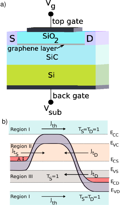
The potential is set to zero at the source and to at the drain contact. In the center of the channel is imposed by vertical electrostatics. We assume, as usual, complete phase randomization along the channel, which is particularly important because it allows us to neglect the effect of resonances in the presence of tunneling barriers.
Exploiting the Gauss theorem we can write the surface charge density in the central part of the channel as
| (2) |
where () is the capacitance per unit area between the channel and the top gate (back gate), () is the top gate (back gate) voltage, () is the flat-band voltage of the top gate (back gate), which we set to eV.
The transit time of the device in the channel has been estimated as s where and are the thermionic charge and current, respectively, nm is the channel length.
In certain spectral regions, for example in the valence band when the device is in the off state, carriers are quasi confined by tunneling barriers, and can dwell in the channel for a much longer time and be subject to some degree of inelastic relaxation, even if transport in the conduction band is practically ballistic. To consider this effect, we have therefore included a degree of inelastic scattering that leads to energy relaxation.
In steady-state conditions, considering an infinitesimal element of area in the wave-vectors space, charge distribution in the channel is obtained as a balance between two types of charge exchange processes with the contacts: one elastic, and one inelastic.
We can write the electron charge in the channel as the sum of two contributions: and .
() represents the density of forward (backward) going electrons,
denotes the occupation factors of forward and backward states
in the channel and is the 2-dimensional density of states in the -space.
For each contribution we can write a rate equation in steady-state conditions:
| (3) |
| (4) |
where:
is the occupation factor at the drain (D) and source (S) contacts, and is Fermi-Dirac distribution function.
Let us focus on eq. 3 (similar considerations can be made for eq. 4):
is the tunneling current component injected from source, is instead the drain tunneling current component ejected to the drain, are the transmission probabilities from source/drain contacts to channel and is the group velocity.
and are the reflected current components from source and drain barriers, respectively.
The last term of eqs. 3 and 4 is a thermalization process with the source and drain reservoirs, with characteristic times and , respectively.
The steady-state and can be obtained by solving eq. 3 and eq. 4:
| (5) |
| (6) |
where is the inverse of the crossing time . The same reasoning can be applied to derive the hole occupation factors in the channel .
The charge, to be self-consistently solved with eq.2 in order to obtain the channel potential , is computed through the integration on the BZ
| (7) | |||||
where the total current density is expressed as [18]
| (8) | |||||
The transmission probability () of the interband barrier at source (drain) is zero in the source (drain) band gap and when there is no barrier between source (drain) and channel. When a barrier is present is computed analytically with the WKB approximation, assuming conservation due translational invariance along the direction:
| (9) |
where and are the classical turning points, and is the particle kinetic energy. The same approach is repeated for .
The potential profile between each contact and the central region of the channel is described by an exponential, with characteristic variation length , obtained from evanescent mode analysis [19]. Assuming we obtain:
| (10) |
where is the effective separation between the interfaces of the SiO2 and SiC layers, for which we assume nm [9].
III Electrostatics
From analysis of the electrostatics we can gain a better insight of the device performance limitations. In fact gate voltage control upon the channel potential (of which the subthreshold slope is a measure) is strictly limited by the quantum capacitance of the channel.
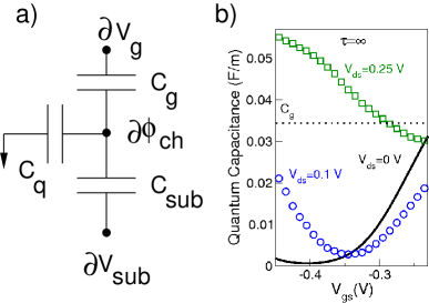
Device electrostatics can be schematized as in 2(a). The differential capacitance seen by the gate is
| (11) |
but, from 2(a), can also be expressed in terms of capacitances , , and :
| (12) |
From eqs. (11) and (12) we get the derivative of the channel potential with respect to the gate potential
| (13) |
The expression of the sub-threshold slope then turns out to be
| (14) |
from which it is clear that is an increasing function of , and therefore a large quantum capacitance severely limits device performance.
2(b) shows the capacitance-gate voltage characteristics for , and V obtained by solving the Schrödinger equation self-consistently with Poisson equation. In the fully ballistic case the quantum capacitance is low for small , indicating a good control of the channel by the gate voltage, but, as soon as increases, hole accumulation in the channel occurs and increases, rapidly degrading (2(b)). In the inelastic case, instead, the hole accumulation process is slightly suppressed by inelastic injection from the source but the effect on the quantum capacitance is practically negligible. We have observed that for larger than ns, the quantum capacitance basically does not change with respect to 2; on the other hand, for ns decreases with respect to the fully ballistic case, but the inelastic process becomes dominant and eq. 14 loses validity.
IV Perspectives for device operation
In order to evaluate the possible performance of the SiC-graphene FET, we have computed the transfer characteristics by varying three device parameters: drain-source voltage , donor molar fraction at the contacts (and therefore parameter ) and oxide thickness . We also account for different possible values of inelastic time . First,in 3, we analyze the trend of the transfer characteristics for different for V, nm and (corresponding to eV).
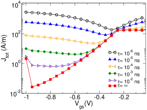
We observe that for ns the transfer characteristics are unaffected and identical to the ballistic case ().
Reducing the relaxation time under ns, the minimum current increases and the sub-threshold slope remains almost constant since the quantum capacitance of the channel does not change.
The introduction of inelastic scattering process has mainly two effects in the transfer characteristics: one is a gradual change of the current in the sub-threshold region, the other is an increase of saturation current for ns or when inelastic current becomes relevant.
In the most favorable case a sub-threshold slope of mV/dec can be obtained.
In 4 we have highlighted the effect of and of the
doping level of contacts.
As expected the main visible effect of increasing is a gradual
degradation of the sub-threshold slope, both in the fully ballistic case
(4(a)-(b)) and in the case of relaxation time ps (4(c)-(d)), from mV/dec to mV/dec.
The reason is simply related to the increased accumulation of holes in the channel with increasing , which implies a larger quantum capacitance of the channel and
therefore a reduced control of the channel potential from the gate voltage.
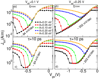
Increasing the doping causes an increase of both the maximum current, due to an improved capacity of the source to inject electrons, and the minimum current. From 4 we draw the indication that by reducing doping at the contacts we improve the current dynamics. As already noted, when the source-drain voltage exceeds the gap of the semiconducting channel ( V), the characteristics drastically degrade, since band-to-band tunneling current becomes comparable with the thermionic current, and hole accumulation in the channel inhibits channel control from the gate.
The increase of oxide thickness has mainly two effects, which can be associated to a reduction of the capacitive coupling between gate and channel: it increases the sub-threshold slope (as shown in 5(a)), and the opacity of tunneling barriers (i.e. a larger ). The former effect is more evident for V, where the quantum capacitance is larger, instead is almost constant at about mV/dec for V and ns, instead for smaller , mV/dec.
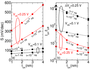
5(b) represents the ratio as a
function of for V and V, calculated
for a gate voltage range V for different values of .
Larger values of the ratio are observed for ns.
From our analysis of transfer characteristics, evaluated by varying three device parameters as , and , we stress the important result that for small and doping level (4(a)) current is modulated by more than 4 orders of magnitude.
We have to stress also the main limitation of graphene on SiC: the energy gap of eV coupled to a low effective mass results in a high band-to-band tunneling current V and so in an increase of the minimum current achievable.
This limitation on affects the perspectives for digital circuit operation: in that case we need and equal to the supply voltage. Even for optimized device parameters ( nm, ), and a supply voltage of 0.25 V, we obtain an
ratio of 50, as can been seen from 5(b).
V Conclusion
In this work we have investigated the performance of field-effect transistors based on epitaxial graphene on a SiC substrate with an analytical model. We have shown that, for small and doping level, current is modulated by more than four orders of magnitude: this is a main improvement with respect to other graphene-based devices [20, 21, 16, 15]. Comparable results can be obtained only with carbon nanotubes or graphene nanoribbons, but only with post-selection of devices after fabrication (for proper chirality and/or width). In the case of graphene on SiC, lithography and device patterning are certainly not prohibitive. A steep subthreshold behavior ( mV/decade) can be obtained for small V, when the accumulation of holes in the channel is inhibited, and a larger current ratio, in excess of , can be obtained for a gate voltage window of V. For digital applications, the limiting factor is represented by the small voltage drop applicable to the channel, being limited by the energy gap ( eV) of the semiconducting material. With optimized device parameters we have obtained a sub-threshold slope of mV/decade and an equal to , with a supply voltage of V and ns. This falls short of requirements of the International Technology Roadmap for Semiconductors, which requires [22]. Finally, we believe that graphene on SiC is very promising as a channel material for FETs, and much attention has to be put on mechanisms capable to suppress hole injection also at larger , that would allow to improve the subthreshold swing and obtain a good also with a small applied voltage, and on its use in tunnel FETs, where its low gap and low effective mass can be turned into an advantage.
Acknowledgements -The work was supported in part by the the CNR and the EC Sixth Framework Programme, under Contract N. ERAS-CT-2003-980409 , through the ESF EUROCORES Programme FoNE-DEWINT, and by the EC Seventh Framework Program under project GRAND (Contract 215752) and the Network of Excellence NANOSIL (Contract 216171).
References
- [1] S. Y. Zhou, G. H. Gweon, A. V. Fedorov, P. N. First, W. A. de Heer, D. H. Lee, F. Guinea, A. Castro Neto, and A. Lanzara, “Substrate-induced bandgap opening in epitaxial graphene,” Nat. Mat., vol. 6, no. 10, p. 770, Oct. 2007.
- [2] X. Peng and R. Ahuja, “Symmetry breaking induced bandgap in epitaxial graphene layers on SiC,” Nano Lett., vol. 8, no. 12, p. 4464, Oct. 2008.
- [3] S. Kim, J. Ihm, H. J. Choi, and Y.-W. Son, “Origin of anomalous electronic structures of epitaxial graphene on Silicon Carbide,” Phys. Rev. Lett., vol. 100, no. 17, p. 176802, 2008.
- [4] V. W. Brar, Y. Zhang, Y. Yayon, T. Ohta, J. L. McChesney, A. Bostwick, E. Rotenberg, K. Horn, and M. F. Crommie, “Scanning tunneling spectroscopy of inhomogeneous electronic structure in monolayer and bilayer graphene on sic,” App. Phys. Lett., vol. 91, no. 12, p. 122102, 2007. [Online]. Available: http://link.aip.org/link/?APL/91/122102/1
- [5] P. Kedzierski, J.and Pei-Lan Hsu; Healey, P. Wyatt, C. Keast, M. Sprinkle, C. Berger, and W. de Heer, “Epitaxial graphene transistors on sic substrates,” IEEE TED, vol. 55, no. 8, p. 2078, 2008.
- [6] K. S. Novoselov, A. K. Geim, S. V. Morozov, D. Jiang, Y. Zhang, S. V. Dubonos, I. V. Grigorieva, and A. A. Firsov, “Electric field effect in atomically thin carbon films,” Science, vol. 306, no. 5696, p. 666, Oct. 2004.
- [7] K. S. Novoselov, A. K. Geim, S. V. Morozov, D. Jiang, M. I. Katsnelson, I. V. Grigorieva, S. V. Dubonos, and A. A. Firsov, “Two-dimensional gas of massless Dirac fermions in graphene,” Nature, vol. 438, no. 7065, p. 197, 2005.
- [8] A. K. Geim and K. S. Novoselov, “The rise of graphene,” Nat. Mat., vol. 6, no. 3, p. 183, Mar. 2007.
- [9] X. Li, X. Wang, L. Zhang, S. Lee, and H. Dai, “Chemically Derived, Ultrasmooth Graphene Nanoribbon Semiconductors,” Science, vol. 319, no. 1229, p. 1150878, 2008.
- [10] F. Schedin, A. K. Geim, S. V. Morozov, E. W. Hill, P. Blake, M. I. Katsnelson, and K. S. Novoselov, “Detection of individual gas molecules adsorbed on graphene,” Nat Mater, vol. 6, no. 9, p. 652, 2007.
- [11] Y.-W. Son, M. L. Cohen, and S. G. Louie, “Energy gaps in graphene nanoribbons,” Phys. Rev. Lett., vol. 97, no. 21, p. 216803, 2006.
- [12] R. Martel, T. Schmidt, H. R. Shea, T. Hertel, and P. Avouris, “Single- and multi-wall carbon nanotube field-effect transistors,” App. Phys. Lett., vol. 73, no. 17, p. 2447, 1998. [Online]. Available: http://link.aip.org/link/?APL/73/2447/1
- [13] B. Biel, X. Blase, F. Triozon, and S. Roche, “Anomalous doping effects on charge transport in graphene nanoribbons,” Phys. Rev. Lett., vol. 102, no. 9, p. 096803, 2009. [Online]. Available: http://link.aps.org/abstract/PRL/v102/e096803
- [14] T. Ohta, A. Bostwick, T. Seyller, K. Horn, and E. Rotenberg, “Controlling the electronic structure of bilayer graphene,” Science, vol. 313, no. 5789, pp. 951–954, August 2006.
- [15] G. Fiori and G. Iannaccone, “On the possibility of tunable-gap bilayer graphene FET,” IEEE EDL, vol. 30, no. 3, p. 261, Mar. 2009.
- [16] Y. Q. Wu, P. D. Ye, M. A. Capano, Y. Xuan, Y. Sui, M. Qi, J. A. Cooper, T. Shen, D. Pandey, G. Prakash, and R. Reifenberger, “Top-gated graphene field-effect-transistors formed by decomposition of sic,” App. Phys. Lett., vol. 92, no. 9, p. 092102, 2008.
- [17] G. Fiori and G. Iannaccone, “Simulation of graphene nanoribbon field-effect transistors,” IEEE EDL, vol. 28, no. 8, p. 760, 2007.
- [18] M. Buttiker, “Coherent and sequential tunneling in series barriers,” IBM J.Res.Dev., vol. 32, no. 1, p. 63, 1988.
- [19] S.-H. Oh, D. Monroe, and J. Hergenrother, “Analytic description of short-channel effects in fully-depleted double-gate and cylindrical, surrounding-gate mosfets,” IEEE EDL, vol. 21, no. 9, p. 445, Sep. 2000.
- [20] M. Lemme, T. Echtermeyer, M. Baus, and H. Kurz, “A graphene field-effect device,” IEEE EDL, vol. 28, no. 4, p. 282, April 2007.
- [21] X. Liang, Z. Fu, and S. Y. Chou, “Graphene transistors fabricated via transfer-printing in device active-areas on large wafer,” Nano Lett., vol. 7, no. 12, p. 3840, December 2007. [Online]. Available: http://dx.doi.org/10.1021/nl072566s
- [22] “International technology roadmap for semiconductor 2007.” [Online]. Available: http://public.itrs.net.