Contactless photoconductivity measurements on (Si) nanowires
Abstract
Conducting nanowires possess remarkable physical properties unattainable in bulk materials. However our understanding of their transport properties is limited by the difficulty of connecting them electrically. In this Letter we investigate phototransport in both bulk silicon and silicon nanowires using a superconducting multimode resonator operating at frequencies between and GHz. We find that whereas the bulk Si response is mainly dissipative, the nanowires exhibit a large dielectric polarizability. This technique is contactless and can be applied to many other semiconducting nanowires and molecules. Our approach also allows to investigate the coupling of electron transport to surface acoustic waves in bulk Si and to electro-mechanical resonances in the nanowires.
pacs:
73.23.-b, 72.30.+q, 63.22.GhIn recent years transport properties of conducting nanowires attracted a considerable interest. Synthesis of carbon nanotubes and semiconducting nanowires opened the possibility of new mechanical, electronic and optical applications. For example carbon nanotubes allowed to fabricate single electron transistors operating at room temperatures Dekker2001 , and very high quality nano-electromechanical resonators in suspended nanotube samples VanDerZant2009 . Numerous photonics applications were achieved with Si nanowires including microcavities and waveguides Koshida2009 . Despite these successes, our understanding of transport properties of nanowires is limited by our ability to make good ohmic contacts at low temperatures. Thus for carbon nanotubes the nature of electronic transport at low temperatures is still unknown (possibilities include formation of a Luttinger liquid or dynamical coulomb blockade) Bachtold . For more exotic nanowires like DNA, even qualitative information on whether the molecule is conducting or insulating is not reliable Endres .
In this letter, we propose a generic experiment to probe photoconductivity without direct contacts. To this end, we couple nanowires to a multimode electromagnetic (EM) resonator. Light irradiation is used to excite carriers in the nanowires which interact with the EM field of the resonator and change the resonance parameters. We demonstrate this technique in practice, by measuring photo-transport in bulk silicon and Si nanowires.
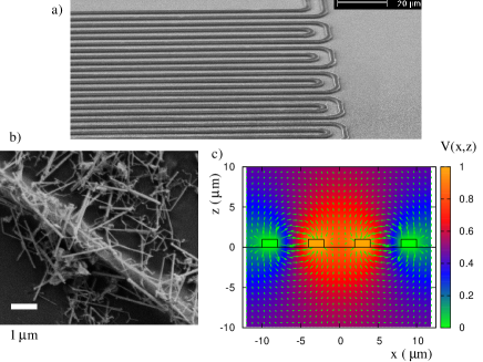
Our probe is a multimode EM resonator formed by two superconducting meanders of total length (see Fig. 1.a). This structure has regularly spaced resonant frequencies given by where and is an integer. The meanders were fabricated by etching a thick niobium film with reactive ion etching. During this procedure the meanders were protected by an aluminum mask patterned using optical lithography. In a last step was dissolved in a KOH solution Reulet1 ; Reulet2 . Two types of dielectric substrates were used. In a first experiment the resonator was prepared on top of a Si/SiO2 substrate (the oxide layer was nm thick), which allowed us to probe conductivity of bulk Si under light irradiation (see Fig. 1.a). In a second experiment we used sapphire as dielectric substrate and we deposited vapour-liquid-solid grown Si nanowires ERouviere on top of the resonator (see Fig. 1.b). Note that sapphire remains insulating under blue irradiation (energy ) due to its high band gap of .
The coupling between the resonator and the Si-nanowires is greatly enhanced by the resonator’s meander structure which strongly confines the EM field near the substrate interface where the nanowires are deposited. We have checked this using a finite element (FEM) calculation of the potential and of the electric field. The results of the simulation are shown on Fig. 1.c, and clearly indicate that the electric field vanishes for where is the distance to the substrate interface (distance between meanders is ). The FEM simulations also show that the electric field is mainly oriented along the interface for .
During the measurements the resonators are immersed in liquid at . The shape and position of the resonances are determined by measuring the reflection along a coaxial cable capacitively coupled to the resonator. At resonant frequencies more power is absorbed by the resonator, and a dip in reflected power is observed (incident microwave power was ). The resonators were then irradiated with a blue light provided by a commercial diode operating at low temperature. For samples on bulk Si the resonances are strongly broadened under irradiation, a typical behavior is shown in Fig. 2.b for the first harmonic of the resonator while no broadening was observed for a control resonator on a sapphire substrate.
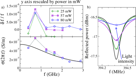
This drop of the resonance quality factor under irradiation can be understood in terms of photoinduced conductivity in Si. Indeed the photon energy of is much larger than the Si gap . Thus the absorption of photons creates a stationary population of electron/holes pairs, and a finite photo-conductivity where is the microwave frequency. In the regime of a weak conductor with the screening is negligible and the associated drop in the resonator quality factor is well described by the relation Landau :
| (1) |
Here is dielectric constant in Si, and the last equality in Eq. (1) is a Drude approximation to with elastic relaxation time . The quantity is the difference between with and without irradiation. The experimental values for are shown on Fig. 2, the quality factors are determined using both amplitude and phase of the reflection coefficient to remove the artificial broadening of the resonance induced by the coupling to the transmission line. Since the excited carrier concentration is proportional to light intensity, we rescale the data of Fig. 2 by the electrical power absorbed by the diode.
A good agreement with Eq. (1) is found for a relaxation time of that corresponds to a mobility (here is the electron mass). From this value the effective carrier temperature can be determined using the mobility dependence on temperature in high purity Si Canali . This effective temperature is determined by the energy transferred by a photon to an electron-hole pair and energy dissipation mechanisms in Si. It does not depend on light power as long as the carrier density remains small (from conductivity data on Fig. 2 we estimate ). The Drude approximation works for all frequencies except for the second resonance at . The relative frequency shift under irradiation has also a peak at . The origin of this resonant frequency can be understood in terms of emission of surface acoustic waves (SAW) in the Si substrate. Indeed the periodic structure of the meanders also creates a resonance for SAW. The corresponding frequency is determined by the distance between meanders and the transverse sound velocity in Si: Wortman , giving a resonant frequency of close to the frequency of the EM resonator. The blue irradiation intensity is also modulated with a period by the presence of the resonator and the continuous excitation of electron-hole pairs can create a charge density wave with period strongly increasing the coupling between the acoustic and EM modes. This would explain why SAW resonance appears very clearly in the photoconduction data.
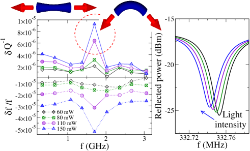
We also used this technique to probe phototransport in Si nanowires (see sample on Fig. 1.b). The typical behavior under irradiation is shown for the first resonance on Fig. 3. Contrarily to samples on bulk Si where only a broadening of the resonance was observed, a shift of the resonance position is clearly visible. In the bulk the charges were not confined in the direction parallel to the Si interface hence only dissipative photoconductive response could be observed. In the nanowires, photo-induced charges are confined and can be polarized, creating a photopolarizability . In order to compare the magnitude of these two effects we assume that we excite at most one electron-hole pair in a nanowire, and we call the surface density of the excited nanowires. The polarization of an excited nanowire is determined from an equilibrium Boltzmann distribution in presence of the resonator electric field : . Here is the nanowire length, is the carrier charge and is the effective carrier temperature. This polarization creates a shift of the resonant frequencies:
| (2) |
where the factor originates from the confinement of the EM field. Photoconductivity is determined by Eq. (1), the unknown conductivity can be estimated with a Drude approximation: where is the effective carrier concentration. The relaxation time is determined by the collisions with the nanowire walls where is the nanowire radius and is the electron mass. Combining these results with Eq. (2) yields the dimensionless ratio :
| (3) |
The quantity does not depend on and thus on light power. This is confirmed by extracting from the data of Fig. 3 which gives typical . After injecting this value in Eq. (3) together with , and we find an effective temperature of the same order of magnitude as in bulk Si.
The frequency dependence in Fig. 3 is characterized by a peak at frequency . The origin of this peak can be related to mechanical resonances in the nanowires, similarly to interaction with SAW for bulk Si. Possible excited modes are shown on top of Fig. 3, and correspond to bending and stretching of the nanowire. For the bending mode resonance occurs when a transverse phonon wavelength fits in a nanowire. For an average nanowire length (length fluctuations are around ) the resonant frequency is . For the stretching mode, only half a wavelength enters the nanowire at resonance, hence the frequency is , where is the longitudinal sound velocity in Si Wortman . The stretching mode gives a better frequency estimate which suggests that mainly this mode is excited in our experiment.
In conclusion we have shown that using a high Q multimode resonator we can probe effectively low temperature photo-transport in bulk Si and Si nanowires. For bulk Si, photo-induced carriers induce a dissipative response which broadens the resonances. The drop of quality factor allows to deduce the relaxation time and the carrier effective temperature. At a special frequency resonant interaction with surface acoustic waves is observed. In Si nanowires, photo-induced carriers can polarize the nanowires and thereby induce a dominant non dissipative response absent in the bulk. We showed that the ratio between dissipative and non-dissipative responses determines the effective carrier temperature in the nanowires. For some special resonant frequencies mechanical resonances in the nanowire could be excited. We stress that this technique is very generic and can be applied to many other systems where photoconductivity is expected, possible examples include DNA and photochromic molecular switches. Coupled with optical spectroscopy, it could provide valuable transport data on nanowires with embedded quantum dots.
We acknowledge ANR QuantADN and NanoTERA for support and thank S. de Franceschi, B. Semin and S. Saranga for help in experiment preparation.
References
- (1) H. W. Ch. Postma, T. Teepen, Z. Yao, M. Grifoni and C. Dekker, Science 293, 76 (2001)
- (2) A.K. Huettel, G.A. Steele, B. Witkamp, M. Poot, L.P. Kouwenhoven and H.S.J. van der Zant, Nano Let. 9, 2547 (2009)
- (3) N. Koshida, “Device Applications of Silicon Nanocrystals and Nanostructures”, Series: Nanostructure Science and Technology, Springer (2009).
- (4) A. Bachtold, M. de Jonge, K.G-Rasmussen, P.L McEulen, M. Buitelaar and C. Schönenberger, PRL 87 166801 (2001)
- (5) R.G. Endres, D.L. Cox and R.R.P. Singh, Rev. Mod. Phys. 76, 195 (2004)
- (6) B. Reulet, M. Ramin, H. Bouchiat and D. Mailly, PRL 75 124 (1995)
- (7) Y. Noat, H. Bouchiat, B. Reulet and D. Mailly, PRL 80, 4955 (1998)
- (8) L. Latu-Romain, C. Mouchet, C. Cayron, E. Rouviere and J-P Simonato J. of NanoParticle Research 10, 1287 (2008)
- (9) L.D. Landau and E.M. Lifshitz “Electrodynamics of continuous media”, Addison-Wesley (1966).
- (10) J.J. Wortman, R.A. Evans, J. Appl. Phys. 36 153 (1965)
- (11) C. Canali, C. Jacoboni, F. Nava, G. Ottaviani, and A. Alberigi-Quaranta, Phys. Rev. B 12, 2265 (1975)