Quantum Size Effects in Pb/Si(111) Thin Films from Density Functional Calculations
Abstract
The Pb/Si(111) thin films were simulated within the density functional theory (DFT). The well-known Perdew-Burke-Ernzerhof (PBE) version of the generalized gradient approximation (GGA) and its recent nonempirical successor Wu-Cohen (WC) issue were used to estimate the exchange-correlation functional. Lattice parameters were calculated for Bulk of the Pb and Si compounds to obtain more reliable lattice mismatch at the interface to be consistent with our used full-potential method of calculations. The WC-GGA result predicts the lattice constants of the Pb and Si compounds better than the GGA when compared with experiment. We have found that the spin-orbit coupling (SOC) does not significantly influence the results. Our finding is in agreement with the recent observation of the Rashba-type spin-orbit splitting of quantum well states in ultrathin Pb/Si(111) films. Our result shows, in agreement with experiment, that the top site (T1) is the most stable phase. A combination of tight and feeble bonds has been found at the interface, which results in a covalent Pb-Si bond. Our calculated electric field gradient (EFG) predicts quantum size effects (QSE) with respect to the number of deposited Pb layers on the Si substrate. The QSE prediction shows that the EFG dramatically drops on going from first to second layer. The EFG calculation shows that this system is not an ideal paradigm to freestanding films.
pacs:
71.15.Mb, 73.20.At, 76.80.+yI Introduction
The Pb/Si(111) thin films can be considered as an ideal interface, since it is an unreactive metal-semiconductor system which forms perfectly an abrupt interface without intermixing.Lay91 Intensive experimentalWei92 ; Sve08 and theoreticalCha03 ; Cha06 works performed on this system show that it is a subject of intense technological and scientific interest with a wide range of applications. Several structures were proposed experimentally for this system.Lay91 ; See95 The structures vary with their circumstances. The variations form a complicated phase diagram. The stability of the proposed structural models were studied theoretically employing pseudopotential calculations.Cha03 The complex phase diagram shows that there are 4 structures with a simple (11)-unit cell. The experimentally observedSel00 simple unit cell provides a suitable case to perform accurate atomic relaxations within an all-electron calculation reliably. Our full-potential surface calculations were then devoted to study these (11) structures with the concentration on their most stable phase. Quantum size effects (QSEs) in nanostructures, e.g., a two-dimensional (2D) ultrathin metal films, appear as dramatic oscillations in many physical properties upon variation of film thickness.Tri07 ; Vaz09 The motion of electrons in the film plane of such a 2D-system is essentially free, whereas the electrons are confined in the normal direction to the film surface, which leads to the quantized electronic states, i.e., quantum well states (QWS).Jia07 The oscillation period was found to be 7-monolayer-height-islands of lead grown on top of a silicon substrate for the electron intensity curve as a function of the normal component of the electron momentum transfer.Tri07 Vázquez de Parga and coworkers observed the QSEs for a number of surface properties, i.e., the surface roughening temperature, work function, chemical reactivity, or the surface diffusion barrier, in the Pb/Si(111) and Pb/Cu(111) thin films by Scanning Tunneling Microscopy/Spectroscopy (STM/STS).Vaz09 The step height of layer N is related to the electron spillage length into the vacuum which depends on the DOS at the Fermi level.Vaz09 Quantum size effects (QSEs) were found for the total energies and energy differences in freestanding Pb(111) thin films by using pseudopotential method as embodied in the CASTEP code.Mat01 Influence of the Cu(111) substrate on the geometry structure of the Pb(111) layers was also indirectly taken into account by solely reducing in-plane lattice constant to impose 3.3% lateral compression on all the Pb(111) layers to mimic the role of Cu(111) substrate.Mat01 The effects of Cu(111) substrate were found to be substantial, as the step heights were calculated to be in more agreement with experiment within the later in-pane strain.Mat01 Wei and Chou theoretically, employing ultrasoft pseudopotential calculations, studied the quantum size effects (QSEs) in the clean surface of Pb(111).Wei02 Recently P. S. Kirchmann et al. experimentally observed quantum size effects (QSEs) in the Pb/Si(111).Kir07 TheyKir07 found their experimental results for the actual Pb/Si(111) slab to be in agreement with the pseudopotential resultsWei02 for the hypothetical freestanding Pb(111) slab. Dil et al.Dil07 comparing their Pb/C full-potential calculations with the Pb/Si(111) experimental results of the othersUpt04 reported that unlike for Pb on graphite, the Pb overlayer lattice structure is influenced by that of the Si(111). Here we then intend to, going beyond the hypothetical freestanding Pb(111) approximation, quantitatively assess the effects of electronic and crystalline structures of the underlying Si substrate on the deposited Pb films. For this reason we inspect the electronic structures at the interface of the Pb/Si(111) slab. From our electronic structure calculations, we show that there is a mixed state composed of weak and strong bonds between Pb and Si at the interface which results in a strong Pb-Si covalent bond. We aim to investigate whether the substrate can influence the results. In order to accomplish the investigation, we have calculated the work function, energy differences and surface formation energy as a function of number of Pb layers for the -Pb/Si(111). Our result shows that the effect of Si substrate can be of significant importance for some physical quantities depending on their sensitivity to the valence electron charge density. We have observed the quantum size effects (QSEs) for the -Pb/Si(111) thin films. The goal of this work more transparently is achieved by presenting a physical interpretation for our QSE calculations for this system in the electric field gradient (EFG) as an extremely sensitive quantity to the valence electron charge density distribution. We would also examine the effect of spin-orbit coupling (SOC) on our thin films. The result, in agreement with experiment,Hug08 shows that the SOC has a minor effect for the Pb/Si(111) thin films. Low temperature , 33 and phases of Pb/Si(111) were theoretically studied employing pseudopotential method.Cud08 It was shown that there could be a discrepancy in predicting the ground state of Pb/Si(111) system between local density approximation (LDA) and generalized gradient approximations (GGA).Cud08 Another objective of our density functional theoryHoh64 ; Koh65 (DFT) calculations is to go beyond the LDA and GGA by using the nonempirical GGA recently proposed by Wu-Cohen (WC) for the exchange-correlation functional,Wu06 which is expected to improve metal surface formation energy and lattice constant calculationsWu06 ; Tra07 compared to the Perdew-Burke-Ernzerhof GGA (PBE-GGA).Per96
II Computational Details
State-of-the-art calculations were performed within the density functional theoryHoh64 ; Koh65 (DFT) as implemented in the WIEN2k code.Bla01 The augmented plane waves plus local orbital (APW+lo) methodSjs00 ; Mad01 has been used for solving the Kohn-Sham equationsKoh65 employing the latest version of the generalized gradient approximation (GGA), i.e., Wu-Cohen (WC), for the exchange-correlation functionalWu06 . We set the Muffin-tin radii to for the Si and to for the Pb atoms. The expansion of the wave functions and charge densities were cut off by the and parameters, respectively. The full relaxations were performed with the criterion of 1 mRy/bohr on the exerted forces. The relativistic effects were taken into account by including the spin-orbit coupling (SOC) in a second variational procedure. A set of special k points has been used for integrations over the Brillouin zone of the 11 surface cell.
III Bulk Structural Properties
| Method | XC-Potential | (bohr) | (Gpa) | |||||
|---|---|---|---|---|---|---|---|---|
| APW+lo | GGA-WC | 10.28 (9.31) | 93 (47.3) | 4.23 (2.9) | ||||
| APW+lo | GGA-PBE | 10.34 (9.49) | 88 (42.2) | 4.16 (5.0) | ||||
| APW+lo | LDA | 10.22 (9.21) | 96 (53.1) | 4.37 (3.7) | ||||
| PPW | LDAa(b) | 10.17 (9.16) | 87 (52.6) | 3.82 (5.2) | ||||
| PPW | GGAc(b) | 10.32 (9.56) | 87 (39.3) | —– (4.7) | ||||
| Exp.d(e) | 10.26 (9.36) | 98 (43.2) | 4.02(4.9) |
Before going through the interface and surface calculations in detail, it seems advisable to first shortly report on the bulk structural properties. In this case, the accuracy of our calculations could be first assessed, and second more accurate lattice parameters would be also obtained to simulate the substrate with an actual and reliable lattice mismatch at the interface. Furthermore one aims to get more insight into the various exchange-correlation functionals, specially the recent proposed WC-GGAWu06 potential. The lattice parameters, bulk moduli, and the pressure derivative of the bulk moduli were calculated for the bulks of the Si and Pb compounds. The calculations were performed within the LDAKur99 , PBE-GGAPer96 and WC-GGAWu06 functionals by fitting the total energy as a function of volume with the Birch equation of state.Bir78 The current APW+lo and previous pseudopotential plane wave (PPW) resultsCam88 ; Yu04 ; Pal99 along with the experimental data Bea70 ; Voh90 are presented in Tab. 1. Our APW+lo result, compared to the experimentBea70 ; Voh90 , shows that, for both the Si and Pb cases, the PBE-GGAPer96 overestimates the lattice constants and bulk modulii, whereas the LDAKur99 underestimates them. This is consistent with the general features of the PBE-GGAPer96 and LDAKur99 functionals for solid states. In particular, as shown in Tab. 1, our values are in complete accord with the previous PPW results.Cam88 ; Yu04 ; Pal99 The WC-GGAWu06 predicts the lattice constant of the Pb compound better than the LDAKur99 and GGA regardless of the APW+lo or PPW method, while our PBE-GGAPer96 remains superior for the prediction of its bulk modulus. This can also be the case for the lattice parameter of the Si compound. From the result presented in Tab. 1 one can cautiously state that the WC-GGAWu06 functional improves the lattice parameters over both the LDAKur99 and PBE-GGAPer96 . This statement is in agreement with the prediction of Wu and Cohen for the most of their studied compoundsWu06 . Our results show that lattice parameters calculated from WC-GGAWu06 approximation are very close to experimentBea70 ; Voh90 . The calculated lattice parameter of the bulk Si, i.e., 10.28 a.u., will be used in the forthcoming Sec. IV for simulating this compound as our substrate to mimic the effects of the lattice mismatch on the valence bands at the interface of the Pb/Si(111). Finally, keeping in mind that the value obtained for the pressure derivative of the bulk modulus depends on the range of fitting and as a result quantitative analysis may not be completely reliable, our result shows that the PBE-GGAPer96 yields better pressure derivatives of the bulk moduli for the Pb and Si compounds than LDAKur99 and WC-GGAWu06 .
IV Slab Determination and Optimization
| (eV) | (eV/) | |||
|---|---|---|---|---|
| 4 | 4.8484 | 1.3037 | ||
| 6 | 4.7179 | 1.3281 | ||
| 8 | 4.7295 | 1.3274 | ||
| 10 | 4.7299 | 1.3270 |
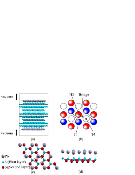
The silicon substrate has been simulated using the calculated WC-GGAWu06 lattice parameter in the previous Sec. III along the (111) crystallographic direction of the space group. We have found that the Si(111) substrate, as shown in Fig. 1(a), can be properly modeled by stacking 8 Si bilayers, i.e., 16 Si monolayers. Surface formation energy, , per unit area and work function, , were calculated for the various number of Si(111) bilayers, , and the results are listed in Tab. 2. Our result shows that the changes of the work function and the surface formation energy are less than 0.001 eV by adding more bilayers. The reliability of the obtained 8 Si bilayers has been further investigated by comparing the bulk and surface electronic structures of the silicon. The total densities of states (DOSs) were calculated for both the bulk and surface of the Si. One expects to observe similar DOSs for the bulk of Si and the deepest atom from the surface of the Si(111). Our calculated surface DOS for predicts a wrong metallic behavior for the deepest Si atom. However, our result confirms that the DOS of the deepest Si layer approaches to the bulk DOS of the Si semiconductor by approaching to the 8 bilayers. We avoid to present the DOSs of the substrate without the deposited Pb layers in this paper, as we just used them to ensure the validity of the Pb/Si(111) thin films calculations. The Pb layers were then deposited over and below the prepared Si(111) substrate to create a symmetric Pb/Si(111) slab. In order to simulate the Pb/Si(111) thin films, the created Pb/Si(111) slab, as shown in Fig. 1(a), is symmetrically immersed in a vacuum as well. The symmetric thin films causes to add inversion symmetry which gives rise to speed up the interface relaxation. The vacuum thickness is defined to be the distance between the top edge of the slab and the bottom edge of its next neighbor. In order to determine the vacuum thickness, total energy, work function and exerted forces on the surface atoms were calculated for the 8 bilayers Si(111) structure versus various vacuum thicknesses. Our results, which are not presented here, show that 12 is sufficient for the vacuum thickness to avoid interactions with the nearest neighbors of the slab along the Cartesian z axis. The total energy, work function and forces were well converged in the vicinity of the obtained vacuum thickness – they did not show significant changes by increasing the vacuum thickness more than the value obtained. All the Si underneath atoms and Pb adatoms are allowed to fully relax by adjusting their heights, but not their coordinates parallel to the Si(111) surface. The top (T1), fcc (T4), hcp (H3), and bridge (B2 – intermediate point of the T1 and T4 or T1 and H3) sites, as corresponding phases for the deposition of the Pb layers on the Si(111) surface, are shown in Fig. 1(b). In order to better visualize the most stable phase, top and cross views of the ()-unit cell of the T1 phase are illustrated in Figs. 1(c) and (d), respectively. In this phase, as shown in Fig. 1(d), the Pb adatoms were positioned along the first layer of the the first Si(111) bilayers. The (11)-unit cell as the interface structure for our full-potential all electron ab initio calculations is outlined in Figs. 1(b) and (c).
V Interface Properties
V.1 Stability
| SOC | T1 (eV) | T4 (eV) | H3 (eV) | |
|---|---|---|---|---|
| No | 0.00 | 0.41 | 0.32 | |
| Yes | 0.00 | 0.25 | 0.20 | |
| Noa | 0.00 | 0.35 | 0.18 |
In this section, we would make sure about the most preferable configuration. Total energies were then calculated for all of the illustrated structures in the Fig. 1(b), apart from the bridge-site structure. The calculations were performed in the presence and absence of the spin-orbit coupling (SOC). Total energies relative to the T1 site are presented in Table. 3. Our result with and without SOC shows that the T1 site is the most stable structure among the other configurations. This result is in agreement with experiment.See95 The energy, as shown in Table. 3, increases from T1 site to T4 site and deceases from T4 site to H3 site. The later trend, as shown in Table. 3, is not affected by the spin-orbit interactions. The result shows that the effect of spin-orbit interactions, keeping the trend, is to shift downward total energies of all the sites. Our results are also quantitatively comparable with the pseudopotential calculations.Bro02 The energy of the bridge-site phase has not been calculated, since, as mentioned in the previous Sec. IV, B2 is an intermediate site of T1 and T4 sites or T1 and H3 sites. Therefore, one can most likely predict that the surface formation energy of the B2 site because of its symmetry is somewhere between T1 and T4 sites or between T1 and H3 sites. This prediction is in complete accord with the pseudopotential results.Bro02 We will concentrate only on the lowest-energy T1 site from later on in the remaining subsequent sections.
V.2 Si-Pb bond length
| Method | XC-Potential | d(Pb-Si) | |
|---|---|---|---|
| FP-APW+lo | WC-GGA | 2.72 | |
| FP-APW+lo | PBE-GGA | 2.70 | |
| FP-APW+lo | LDA | 2.68 | |
| PPWa | LDA | 2.66 | |
| EXP.b |
Bond length of Pb-Si, d(Pb-Si), at the interface of our slab has been calculated for the most energetically stable phase, i.e., T1 site, as shown in Tab. 3. The WC-GGAWu06 , PBE-GGAPer96 and LDAKur99 functionals were used for the exchange-correlation (XC) potential. Our full-potential results together with the pseudopotential results of the othersCha03 as well as experimental dataKum00 are listed in Tab. 4. The experimental data were obtained by surface X-ray diffraction based on the Pb/Si(111)- modelKum00 . This model contains 7 Pb adatoms in the -unit cellKum00 . Here we are only interested in the four of these lead atoms, since they are located in the top (T1) site as our predicted most stable phaseKum00 . The Pb-Si bond lengths for these 4 lead adatoms were measuredKum00 to be between and .Kum00 The covalent radii of silicon and lead are and , respectively, and the bulk radius of lead is .Kum00 Thereby the covalent bond lengths of Pb-Si have to be between and , viz. .Kum00 Our LDA full-potential result, as shown in Tab. 4, is in excellent agreement with the LDA pseudopotential result of the others.Cha03 The LDA results, as shown in Tab. 4, are very close to the strongest covalent bond length, i.e., . The result demonstrates that the PBE-GGA and WC-GGA give larger bond lengths which result in weaker Pb-Si bonds than LDA. This confirms a trend shown in Tab. 1 in which the LDA underestimates but GGA overestimates lattice parameters compared to experiment. The weaker PBE- and WC-GGA bonds, as shown in Tab. 4, are still in the covalent bond length interval, i.e. [2.65, 2.93 ]. The predicted covalent bonds by LDA and GGA show that the competition between the Pb-Si and Pb-Pb interactions gives rise to saturate all the dangling bonds of the silicon substrate. Finally, it worths to mention that the trend seen in Tab. 1 is reversed here, as shown in Tab. 4, between PBE-GGA and WC-GGA in which PBE-GGA predicts lattice parameter larger than WC-GGA. In contrast to the lattice parameter trend, here, as shown in Tab. 4, the Pb-Si bond length within the WC-GGA is slightly larger than the Pb-Si bond length within the PBE-GGA. Normal and in-plane Pb-Si distances, viz. and , were calculated employing pseudopotential method for the mixed phase obtained from coadsorption of Pb and Sn on the Si(111) surface. The Pb-Si bond lengths, d = , were found to vary from 2.77 Å to 3.33 Å depending on the positions of silicon atoms with respect to the lead adatoms for the (Pb, Sn)/Si(111) phase.Cud08 The Pb-Si bond length of the later model with less in-plane Pb-Si distance can be more comparable with the bond length obtained from our top site phase. The less in-plane distance and its corresponding normal distance were calculated to be = 1.79 Å and = 2.11 Å, respectively, which resulted in Pb-Si bond length d = = 2.77 Å.Cud08 The later bond length, 2.77 Å, which is in the above mentioned covalent bond length interval, i.e., [2.65, 2.93 ] and closer to our WC-GGA result, asserts that the Pb-Si forms a very strong bond.Cud08
V.3 Work function and surface formation energy
| Method | XC-Pot. | SOC | Si(111) | (eV) | (eV/) | |
|---|---|---|---|---|---|---|
| FP-APW+lo | WC-GGA | No | Yes | 4.72 | -0.59 | |
| FP-APW+lo | WC-GGA | Yes | Yes | 4.65 | -0.61 | |
| FP-APW+loa | WC-GGA | No | No | 4.23 | 0.02 | |
| PPWb | LDA | No | Yes | —– | -0.47 | |
| PPWc | PW-GGA | No | No | 4.07 | —– | |
| PAW-PPWd | GGA92 | No | No | 3.83 | 0.03 |
aThese free-standing Pb(111) values are given for N=2. For N=1, the hypothetical free-standing film is so unstable that may no longer be considered as a physical system even within a pure theoretical study.
The given surface formation energy in the reference Sun08, , 0.372 eV, is converted from eV to eV/. Hence the value of 0.372 eV is divided by the area of the -unit cell, 12.804 .
We calculated the work function ,, as the minimum energy required to liberate an electron from the Fermi level () to a point with negligible kinetic energy at the center of the vacuum of the slab. The calculations were performed using the following formula:
| (1) |
where is estimated by the averaged electrostatic Coulomb potential at the midpoint of the vacuum of the slab and is the corresponding Fermi energy. The work function is a sensitive parameter to the surface conditions, since the liberated electron must move through the surface. The work functions were calculated at the interface of the slab with and without SOC and the results are presented in Tab. 5. The result shows that the SOC causes to reduce the work function. The pseudopotential results for the clean Pb(111) surfaceJia06 ; Sun08 are also given in Tab. 5 within two different exchange-correlation functionals. The comparison shows that the various versions of GGA can result in slightly different values. Since the pseudopotential work functions are available for the hypothetical free-standing Pb(111), we also added our results without Si(111) substrate in Tab. 5 for the comparison. Our free-standing work function is calculated for the second layer of the Pb(111). A single lead layer without any substrate may not constitute a meaningful stable physical system. Our Pb(111) work function which is in good agreement with the pseudopotential result would be compared with the results of our actual Pb/Si(111) slab to elucidate the role of Si(111) substrate. An overlook on the Tab. 5 shows that our calculated work functions taking silicon substrate into account are in the same order of magnitudes when compared to the free-standing full- and/or pseudo-potential results. From the later point, it appears that the Si substrate does not significantly influence the work functions. The later point confirms the observation of P. S. Kirchmann et al.,Kir07 , where theyKir07 found the agreement between their experimental QSE observation for the actual Pb/Si(111) and the pseudopotential resultsWei02 for the hypothetical freestanding Pb(111).
The surface formation energy per unit area at zero temperature is defined as:Pen00
| (2) |
where is the total energy of the slab, () and () are the number and bulk energy of the Si (Pb) atoms in the unit cell, respectively. Here A is the area of the (11)-unit cell. The factor is used in the above formula, since the slab has two surfaces, as shown in Fig. 1(a), due to the embodied inversion symmetry. In principle one can use the above equation as the standard method to calculate the surface formation energy. However, it is well known that in practice the surface formation energy employing Equ. 2 diverges.Fio96 ; Boe98 In order to overcome the divergence problem of the standard Equ. 2, in this paper we have used the following formulaFio96 to calculate the surface formation energy:
| (3) |
where and . We have already used Equ. 3, with , in the previous Sec. IV to calculate the surface formation energy of the pure Si(111) substrate. Our calculated surface formation energies in the presence and absence of the spin-orbit coupling (SOC) along with the pseudopotential results for both of the actual Pb/Si(111) interfaceCha03 and hypothetical clean Pb(111) surfaceSun08 are given in Tab. 5. Our result shows that the effect of SOC is small as well. Spin-orbit (SO) coupling breaks down the space inversion symmetry by imposing a preferable direction, which gives rise to spin splitting. The inversion symmetry can be also broken at an interface or a surface. The Rashba-effectByc84 on metallic surfaces is a phenomenon, which originates both from spin-orbit coupling and the lack of inversion symmetry at surfaces.Bih06 A Rashba-type spin-orbit splitting with no coverage dependency was found for quantum well states formed in ultrathin Pb films on Si (111).Hug08 Hugo Dil et al.Hug08 found for the states at 0.15 and 0.4 eV this splitting to be 14 and 15 meV, respectively. We found the same splitting in the vicinity of Fermi level for the valence bands. The SO coupling within this small splitting, as shown in Tab. 5, causes to reduce the work function and surface formation energy by 0.07 eV and 0.02 eV/, respectively. As shown in Tab. 5, the surface formation energy is a negative value taking substrate into account, i.e., for the actual Pb/Si(111) case. On the contrary it is a tiny positive value without substrate, i.e., for the hypothetical freestanding Pb(111) case. The obtained negative value when compared with the tiny positive value confirms that the Pb/Si(111) is energetically more favorable to form that particular structure than the clean Pb(111) surface. The later point is in complete accord with the pseudopotential results, as can be seen from Tab. 5. Therefore, the effect of substrate is obviously to make the Pb layers energetically stable.
V.4 Density of states (DOS)
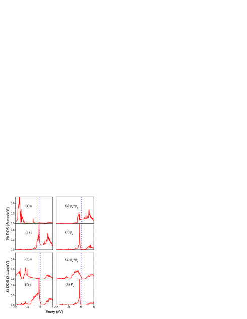
Total and partial densities of states (DOSs) were calculated at the interface for both of the underneath Si and the overlayer Pb atoms. The calculations were performed in the absence and presence of the spin-orbit coupling (SOC) for the slab shown in Fig. 1(a). Total DOSs with and without SOC, which are not shown here, were compared. Despite the large atomic number of Pb, the comparison shows that the effect of SOC is not very significant on the valence electronic structure and can be ignored. This is in accordance with the experiment in which the magnitude of the Rashba-type spin-orbit splitting were found for this thin films to be so small that can be detected by the spin integrated angle resolved photoemission (ARPES) method.Hug08 The spin splitting originates from all of the layers and thereby should be calculated by integrating over the entire layers.Hug08 The spin splitting is small in Pb/Si(111) ultrathin films, because the signs of the splittings of the Pb-vacuum and Si(111)-Pb interfaces are opposite in direction due to the larger phase shift at the Pb to the vacuum interface than the phase shift at the Pb to Si(111) interface.Hug08 Thus the total splitting which partly cancels each other results in an ignorable spin-orbit coupling effect in Pb/Si(111). Therefore from now on we do not include the spin-orbit interactions in all of our surface calculations. Partial s and p DOSs are shown in Figs. 2(a) and (b) for Pb and in Figs. 2(e) and (f) for Si atoms at the interface of the slab, respectively. The result shows that the s states of the Pb and Si atoms are almost distributed over the energy interval of (-10, -5) eV, while their p states are nearly in the (-4, = 0) eV energy window. This demonstrates that the s states are lower in energy than the p states for both of these Pb and Si atoms. Consequently, the s states of Pb and Si are more localized than their p states, which are closer to the Fermi level when compared with the former s sates. Since the p orbital manifest itself more closely to the Fermi level, the p sates show more itinerant character than the s sates. Hence, the p electrons play more important role than the s electrons in the Pb-Si bonding. Now we can discuss the kinds and qualitatively the strengths of the Pb-Si bonds, keeping three points in mind: (i) s (p) electrons are more localized (itinerant) than p (s) electrons for both of the Pb and the Si atoms, and (ii) below the Fermi level interval energy (-10, -5) eV of s states do not overlap interval energy (-4, 0) eV of p states for both of the Pb and Si atoms, as well as (iii) Pb sits on-top of Si site vertically along z direction, as shown in the top site configuration in Fig. 1 (b). The result shows that the 6s states of Pb adatoms are weakly hybridized with the 3s states of the Si substrate. According to the above point (ii) the energy window of 3s Si well overlaps the energy window of 6s Pb, as shown in Figs. 2(a) and (e). One may then promptly speculate that the 6s Pb states can be well hybridized with the 3s Si states. However, according to the point (i) both of the 6s and 3s states are nearly localized and so do not substantially contribute in bonding. Thereby the overlap of the 3s Si and 6p Pb DOSs can only result in an extremely weak -like bond, which may be due to its weakness neglected. The 6s Pb states are even much more weakly bonded to the p Si states compared to the former extremely weak -like Pb-Si bond. According to the property (ii) energy windows of 6s Pb and 3s Si do not overlap, because the s-Pb states are over (-10, -5 eV), while the p-Si state are in (-4, 0 eV), as can be clearly seen from Figs. 2(a) and (f). This in turn gives rise to even weaker bond between 6s Pb and p Si states than the last 6s Pb and 3s Si bond. This is also the case, as shown in Figs. 2(b) and (e), for the p Pb and s Si DOSs. Till now, there are no any evidence of the appearance of Pb-Si bonding. Let us then discuss the bonding states by concentrating solely on the most important p states of the Pb and Si. First, the result shows that the energy window of p Pb well overlaps the energy window of p Si, as shown in Figs. 2(b) and (f). Second, according to the above mentioned (i) point, the p Pb and Si electrons are more itinerant than their s electrons. Third, there are a lot of p Pb and p Si states at an energy very close to the Fermi level, see two sharp peaks in Figs. 2(b) and (f). Therefore, the p states of the Pb and Si atoms can be well hybridized with each other. In order to determine the kind of Pb-Si bond, the p states of Pb and Si were further decomposed, as shown in the right panel of the Figs. 2, to their partial and states. The distributions of the and DOSs of both Pb and Si atoms show that they are completely hybridized with each other. Here, the z axis is taken to be perpendicular on the surface and x,y are parallel to the surface. The Pb overlayer atom is just located above the Si underneath atom along the z-Cartesian coordinate in the top site configuration, as shown in Figs. 1(b). Hence, one lobe of the orbital of Si underneath atom overlaps with one lobe of the orbital of Pb overlayer atom. Consequently, hybridization of orbitals of Pb and Si results in a -bond. The strength of the Pb and Si -bond can be estimated by observing that the two sharp peaks at an almost single energy nearby the Fermi level originate from the Pb and Si DOSs, as shown in Figs. 2(d) and (h). This can be taken as an indication to the fact that there is a tightly -bond between the the Pb and Si at the interface. This result is in excellent agreement with the pseudopotential result of the othersCud08 for Pb/Si(111) phase, in which a strong hybridization between the Pb orbital and the dangeling bonds of the substrate had been reported. As shown in Figs. 2(c) and (g), two lobes of the Pb overlap with two lobes of the Si as well, which gives rise to a -bond. The strength of the -bond cannot be so large, because the Pb and Si DOSs are broadened, as shown in Figs. 2(d) and (h), in contrast to the sharp narrow Pb and Si DOSs. Thereby, a feeble -bond is constituted by the the Pb and Si at the interface. We conclude this discussion by stating the following points. There is not a pure or state in the Pb-Si bond. Instead there is a mixed state composed of and states in the Pb-Si bond. The combination of these two feeble and strong bonds can result in a strong covalent Pb-Si bond. The later point is consistent with our last discussion in Sec. V.2 regarding the bond length of Pb-Si. In summary, the Pb overlayer can be strongly absorbed by the Si substrate.
VI Thin Films Properties
VI.1 Total Energy and Energy Differences
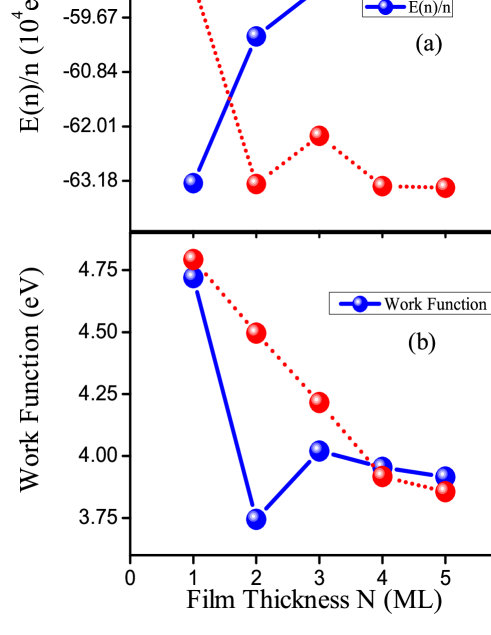
Total energy per number of layers, , is shown in Fig. 3 (a) as a function of the film thickness, N. The result shows that the increases by N and asymptotically approaches to a constant value. The asymptotic behavior can be realized, if we notice that the motion of Pb electrons is confined in one direction while it remains free to move on the surface. The later point itself is due to the fact that the Pb/Si(111) is a prototype of the metal-on-semiconductor system with a high Schottky barrier against penetrating valence electrons of Pb into the substrate.Hes90 ; Cvi02 The confinement in the nanoscale causes wave vector k to quantize in a perpendicular direction on the surface, which results in discrete energy levels associated with the so-called quantum-well (QW) states. The simplest way to describe this confinement is then by the one dimensional QW.Chi00 In a direction normal on the surface there is no translation symmetry. The potential in the xy plane is periodic and potential in the z direction represents the QW. The energy levels in the free electron approximation are given by:
| (4) |
where is the free electron mass and d is the thickness of the film. The above equation clearly shows that the total energy approaches to a constant value by increasing the film thickness. This equation elucidates recognition of the asymptotic behavior shown in Fig. 3 (a). Monolayer per atom energies were calculated for the freestanding Pb(111) slab as a function of monolayers N.Mat01 In agreement with our above discussed asymptotic behavior for the actual case of Pb/Si(111), it was shown that of the hypothetical freestanding Pb(111) system gradually approaches a constant value.Mat01
The energy difference between two successive layers is defined as:
| (5) |
The versus number of layers, N, is also shown in Fig. 3(a). The result shows that the energy difference oscillates as a function of the number of monolayer (ML) coverages with the period of . The oscillation is attributed to the quantum size effect (QSE). Similar QSEs were detected by the pseudopotential calculations for the freestanding Pb(111) thin films.Mat01 One expects that the underlying physics behind of the observed QSE in the quantity, as shown in Fig. 3(a), can be related to the electronic structure of the system. We would postpone this point to a more appropriate time in Sec. VI.3, where the electric field gradient (EFG) as an extremely sensitive quantity to the valence electron charge density distribution is discussed.
VI.2 Work function and surface formation energy
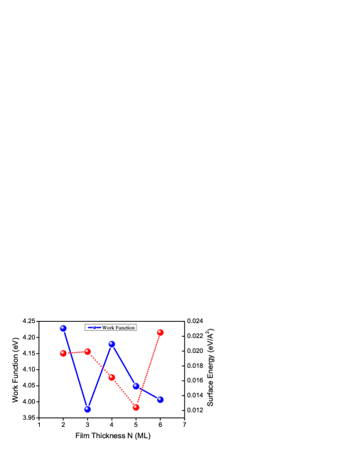
The work function, as discussed in the previous Sec. V.3, has been calculated utilizing Equ. 1. The result is presented in Fig. 3(b) as a function of Pb thin films thickness for the actual Pb/Si(111) slab. The result shows an oscillatory behavior of the work function versus the film thickness with the period of . The oscillation is quickly damped and the work function is going to be converged through a few number of Pb layers. The work function oscillation was previously attributed to the quantum size effects (QSE) and predictedWei02 by using a pseudopotential calculation for the case of a freestanding Pb slab. The pseudopotential resultWei02 for the hypothetical clean Pb(111) thin films shows that the oscillation is much more slowly damped and the work function is converged at a very large number of Pb layers when compared with our full-potential results for the real Pb/Si(111) case. The different oscillatory behavior might be related to the effect of the Si substrate. But one has to notice that the discrepancy may come from the two different approaches. Thus we calculated the work function for the clean Pb(111) surface within our full-potential method as well. The result as shown in Fig. 4 shows that our full-potential work functions are also no longer rapidly damped for the clean Pb(111) case in agreement with the pseudopotential result. This verifies that the oscillatory behavior discrepancy indeed results mainly from the existence and extinction of the Si substrate and not from the method of calculations. This authenticates that the occurred QSE in the work function is influenced by that of Si(111). The effect of Si substrate on the work function confirms the calculation of Dil et al.,Dil07 where theyDil07 similarly found that unlike for Pb on graphite, the Pb overlayer lattice structure is influenced by the Si(111). The effect of our Si(111) substrate on both of the geometry and electronic structures of the Pb overlayer atoms is also in agreement with the influence of the Cu(111) substrate on the geometry structure of the Pb(111) layers reported by Materzanini and coworkers.Mat01 In the later work, the effect of substrate was studied in a tricky manner without including directly Cu(111) underneath atoms by compressing the supercell dimensions in the surface plane by 3.3%.Mat01 They found that the explicit inclusion of the Cu(111) substrate would be highly desirable to explain the remaining quantitative differences between theory and experiment.Mat01 It seems that the later result contradicts our last finding in Sec. V.3. We found in Sec. V.3 that the order of magnitude of the work function could not be significantly affected by the substrate in agreement with the observation presented in Ref. Kir07, . The contradiction can be resolved if we notice that the work function is not so sensitive that its order of magnetite, but its oscillatory behavior, can be affected by the substrate. The electric field gradient (EFG) is much more sensitive quantity than the work function to the surface states. We shall show in subsequent Sec. VI.3 that the EFG is so sensitive to the substrate that not only its oscillatory behavior but also its value can be affected by the Si substrate.
We calculated the surface formation energy versus the film thickness, N, based on the Equ. 2. The result, which is not shown here, varies linearly with respect to N. The linear variation is consistent with the first scheme described in Ref. Fio96, . We then recalculated the surface formation energy versus N according to the Equ. 3. The result, as shown in Fig. 3(b), manifests a deviation from the linear behavior on going from fourth to the fifth layer. The deviation is consistent with the third scheme discussed in Ref. Fio96, . Here we did not use the fourth scheme given in Ref. Fio96, . According to the fourth scheme the Bulk energies in the standard Equ. 2 can be found by taking the slope of a fitted straight line to all of the slab total energies versus N. It is generally believedFio96 ; Boe98 ; Hon03 that the divergence problem disappears employing the fourth scheme for smaller N. However, in this paper we aim to elucidate the role of substrate. The goal of this paper can be achieved even by the third scheme which is identical to the the Equ. 3. Therefore we calculated the surface formation energy versus N for the clean Pb(111) surface. The result is shown in Fig 4 which can be compared with the surface formation energy of the actual Pb/Si(111) slab as shown in Fig. 3(b). Furthermore the clean Pb(111) surface formation energy behaves completely different from that of its supported slab by the Si substrate. The different behavior demonstrates the effect of Si on the surface formation energy.
VI.3 Electric Field Gradient (EFG)
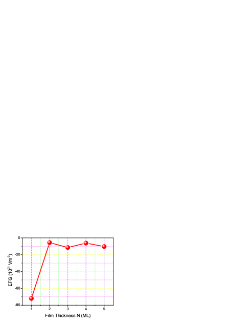
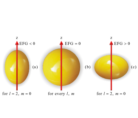
The electric field gradients (EFGs)Bla88 ; Sch90 were calculated at the Pb sites for our slab. The main component of the EFG tensor, , is presented as a function of film thickness, N, in Fig. 5. The sign of the is negative, as shown in Fig. 5, for all the layers. The result shows that for 1 monolayer coverage, i.e., N = 1, the absolute value of the is a very large number. As shown in Fig. 5, the is drastically reduced on going from first to the second layer. Despite the reduction is significant, the values are still considerably large for . Our result shows that for the larger N the oscillates with respect to the number of monolayer (ML) coverages. The period of oscillation here is also . Therefore our ab initio calculations clearly elucidate the quantum size effect (QSE) in the electric field gradient (EFG). In order to interpret the above observation shown in Fig. 5 a cartoonlike electron charge distribution is illustrated in Figs. 6. The electric field gradient (EFG) is an extremely sensitive quantity to the deviation from the spherical valence electron charge density distribution.Sch90 ; Yu91 ; Jal02 ; Jal04 The EFG, as shown in Fig. 6 (b), is zero for a spherical charge density distribution, which is the case for the cubic or higher point group symmetry. The EFG, as shown in Figs. 6 (a) and (c), can be nonzero at an atomic site depending on its point group symmetry for an aspherical charge density distribution, which is the case for our Pb sites. The EFG can be calculated within the APW method by .Las03 The EFG can be nonzero for an aspherical charge density distribution and obtained directly from the l = 2, m = 0 component of the potential expansion inside the muffin-tin spheres.Jal04 The sign of the EFG depends on the orientation of the anisotropic charge density distribution. The sign is defined to be negative (positive) for the charge distribution shown in Fig. 6 (a) (Fig. 6 (c)). Our surface Pb atoms for 1 monolayer (1 ML) coverage are only supported by their underneath Si(111) substrate atoms, since for N = 1 there is no more Pb overlayer on the first deposited Pb layer. The Pb-Pb bonds in the (x, y)-plane compensate each other. However, there is no Pb-Pb bonds along the z Cartesian direction to compete with the Pb-Si bonds to compensate them. The Pb-Si bond, as discussed in Sec. V.2, is a strong covalent bond. The uncompensated covalent Pb-Si bond results in a dramatic electron charge density deformation along the z direction. Consequently one can, according to the Fig. 6 (a), first expect that the sign of the EFG is negative and second its value is dramatically large. These expectations are in excellent agreement with our result as shown in Fig. 5. For 2 ML coverages the second Pb layer is supported by the first Pb layer. The Pb-Pb bonds, which are again compensated in the (x, y)-plane, are much weakerKum00 than the Pb-Si bonds along the z Cartesian direction. The weaker bonds results in a less charge density deformation which gives rise to a less value of the EFG at the Pb site for the second layer. The later point clearly explains the significant drop of the EFG on going from N = 1 to 2 as shown in Fig. 5. Although the EFG is drastically reduced by adding the second layer, it can be still large due to the anisotropy of the Pb surface. The anisotropy comes from the fact that for N = 2 there is no Pb-Pb bond over the second layer to compensate the Pb-Pb bonds between the first and second layers.
Here we would back to the postponed point to clarify that the source of the quantum size effect (QSE) originates from the electronic structure of the system. In order to reach the purpose one can first make a connection between the EFG and the density of states (DOS). Fortunately an astonishing connection was previously madeJal07 between the EFG and the total DOS at the , . There it was found an approximately linear relation between the main component of the electric field gradient and the total density of states at the Fermi level, viz. , in the compound.Jal07 Therefore from one side there can be a relation between the and the in our thin films. On the other hand here we have shown that the oscillates as a function of film thickness. Consequently, there might be a relation between QSE and the electronic structure, or more specifically, between QSE and the total DOS at the Fermi level (). Our finding regarding the later relation between QSE and verifies the previously reported relation between and the electron spillage length into the vacuum and as a result between and the step height of the layer N.Vaz09 This illuminates the underlying physics behind of the quantum size effects (QSEs). Our EFG study shows that the oscillations of a sensitive physical quantity with respect to the film thickness originates from the beating of the valence electron charge density distributions (VECDD). The VECDD deformation can change layer by layer depending on the bonds strength. The effect of the Si substrate, which is shown to be of significant importance in the strength of the bonds, plays an important role in the QSE. One suspects that the freestanding model can be applicable for those kinds of the thin films that the strength of their substrate-overlayer bonds are comparable with the strength of their overlayer-overlayer bonds. The later point is not the case for our thin films, since the strengths of the Pb-Si and Pb-Pb bonds are not comparable.Kum00 In conclusion our QSE calculation shows that our system is not an ideal paradigm to freestanding films.
VII Conclusions
The effects of Si(111) substrate were investigated on the physical properties of the Pb/Si(111) thin films. The investigations were performed within the density functional theory (DFT) employing the augmented plane waves plus local orbital method (APW+lo). We used the PBE-GGA and WC-GGA for the exchange-correlation functional. Our result shows that the WC-GGA is more reliable to study this system. We included spin-orbit interactions in our the Kohn-Sham Hamiltonian. Our result shows that the effect of spin-orbit coupling is not of significant importance for this thin film. Several structures were considered for the slab. Our ab initio full-potential calculation shows that the top site (T1) is the most stable phase. The electronic structures at the interface of the most stable T1 phase were studied. The study shows that the Pb and Si at the interface are strongly bonded by and weakly by bonds. The strong covalent Pb-Si bond is consistent with experiment. In order to elucidate the role of Si substrate the Quantum size effects (QSEs) were studied for the T1 configuration. The study is carried out by calculating the work function and surface formation energy as well as the electric field gradient (EFG) at the Pb sites. The calculations were performed as functions of the thin film thickness (N). We connected the oscillatory behavior of our calculated physical quantities to the electronic structures at various layers of the system. The connection has been made by the concept of the electric field gradient (EFG) as an extremely sensitive quantity to the electronic structure. The EFG provides a reliable approach to undertake the underlying physics behind of the QSE. Therefore the electric hyperfine interaction has merit as a measurement method to be further used in thin films. Our result shows that the effect of Si substrate depends on the sensitivity of the physical quantities to the valence electron charge densities. The Si substrate can be considerable for the sensitive quantities such as electric filed gradients (EFG), while it can be ignored for less sensitive quantities such as the value of the work function.
Acknowledgements.
This work is supported by University of Isfahan (UI), Isfahan, Iran. We are also thankful to Computational Nanotechnology Supercomputing Center Institute for Research in Fundamental Science (IPM) P.O.Box 19395-5531, Tehran, Iran for the computing facility.References
- (1) G. Le Lay, M. Abraham, A. Kahn, K. Hricovini and J. E. Bonnet, Physica Scripta. T35, 261-267 (1991).
- (2) H. H. Weitering, D. R. Heslinga, and T. Hibma, Phys. Rev. B 45, 5991 (1992).
- (3) M. Švec, P. Jelínek, P. Shukrynau, C. González, V. Cháb and V. Drchal, Phys. Rev. B 77, 125104 (2008).
- (4) Tzu-Liang Chan, C. Z. Wang, M. Hupalo, M. C. Tringides, Zhong-Yi Lu, and K. M. Ho, Phys.Rev. B 68, 045410 (2003).
- (5) T.-L. Chan, C. Z. Wang, M. Hupalo, M. C. Tringides, and K. M. Ho, Phys. Rev. Let. 96, 226102 (2006).
- (6) L. Seehofer, G. Falkenberg, D. Daboul, and R. L. Johnson, Phys. Rev. B 51, 13503 (1995).
- (7) J. Slezák, P. Mutombo, V. Cháb, Surface Science 454-56, 584-590 (2000).
- (8) Michael C. Tringides, Mieczyslaw Jalochowski, and Ernst Bauer, Phys. Today 60 April 50 (2007).
- (9) A.L. Vázquez de Parga, J.J. Hinarejos, F. Calleja, J. Camarero, R. Otero, R. Miranda, Surface Science 603 1389-1396 (2009).
- (10) Giuliana Materzanini, Peter Saalfrank, and Philip J.D. Lindan, Phys. Rev. B 63, 235405 (2001).
- (11) Jin-Feng Jia, Shao-Chun Li, Yan-Feng Zhang, and Qi-Kun Xue , J. Phys. Soc. Jpn. 76, 082001 (2007).
- (12) C. M. Wei, and M. Y. Chou, Phys. Rev B 66, 233408 (2002).
- (13) P. S. Kirchmann, M. Wolf, J. H. Dil, K. Horn, and U. Bovensiepen, Phys. Rev. B 76, 075406 (2007).
- (14) J. H. Dil, T. U. Kampen, B. Hülsen, T. Seyller, and K. Horn, Phys. Rev. B 75, 161401(R) (2007).
- (15) M. H. Upton, C. M.Wei, M.Y. Chou, T. Miller, and T.-C. Chiang, Phys. Rev. Lett. 93, 026802 (2004).
- (16) J. Hugo Dil, Fabian Meier, Jorge Lobo-Checa, Luc Patthey, Gustav Bihlmayer, and Jürg Osterwalder, Phys. Rev. Lett. 101, 266802 (2008).
- (17) P. Cudazzo, G. Profeta, A. Continenza, Surface Science 602, 747-754 (2008).
- (18) P. Hohenberg and W. Kohn, Phys. Rev. 136, 864 (1964).
- (19) W. Kohn and L. J. Sham, Phys. Rev. 140, A1133 (1965).
- (20) Z. Wu, and R. E. Cohen, Phys. Rev. B 73, 235116 (2006).
- (21) Fabien Tran, Robert Laskowski, Peter Blaha, and Karlheinz Schwarz, Phys. Rev. B 75, 115131 (2007).
- (22) J. P. Perdew, K. Burke, and M. Ernzerhof, Phys. Rev. Lett. 77, 3865 (1996).
- (23) P. Blaha, K. Schwarz, G. K. H. Madsen, D. Kvasnicka, and J. Luitz, WIEN2K, ”An Augmented Plane Waves + Local Orbitals Program for Calculating Crystal Properties,” Karlheinz Schwarz, Techn. Universitat Wien, Austria, ISBN 3-9501031-1-2 (2001).
- (24) E. Sjöstedt, L. Nordström, and D. J. Singh, Solid State Commun. 114, 15 (2000).
- (25) G. K. H. Madsen, P. Blaha, K. Schwarz, E. Sjöstedt, and L. Nordström, Phys. Rev. B 64, 195134 (2001).
- (26) S. Kurth, J. P. Perdew, and P. Blaha, Int. J. Quantum Chem. 75, 889 (1999).
- (27) F. Birch, J. Geophys. Res. 83, 1257 (1978).
- (28) P. E. V. Camp, V. E. V. Doren and J. T. Devreese, Phys. Rev. B 38, 12675 (1988).
- (29) Dengke Yu and Matthias Scheffler, Phys. Rev. B 70, 155417 (2004).
- (30) M. Palummo, G. Onida, R. Del Sole and M. Corradini, and L. Reining, Phys. Rev B 60, 11329 (1999).
- (31) A. G. Beattie and J. E. Schirber, Phys. Rev. B 1, 1548 (1970).
- (32) Y. K. Vohra and A. L. Ruoff, Phys. Rev. B 42, 8651 (1990).
- (33) S. Brochard, Emilio Artacho, O. Custance, I. Brihuega, A. M. Baro , J. M. Soler, and J. M. Gómez-Rodríguez, Phys. Rev. B 66, 205403 (2002).
- (34) C. Kumpf, O. Bunk, J. H. Zeysing, M. M. Nielsen, M. Nielsen, R.L. Johnson and R. Feidenhans’l, Surf. Sci. 448, L213 (2000).
- (35) R. Pentcheva, and M. Scheffler, Phys. Rev B 61, 2211 (2000).
- (36) Yu Jia, Biao Wu, H. H. Weitering, and Zhenyu Zhang, Phys. Rev B 74, 035433 (2006).
- (37) Bo Sun, Ping Zhang, Zhigang Wang, Suqing Duan, Xian-Geng Zhao, Xucun Ma, and Qi-Kun Xue, Phys. Rev B 78, 035421 (2008).
- (38) Vincenzo Fiorentiniy and M Methfessel, J. Phys.: Condens. Matter 8, 6525-6529 (1996).
- (39) J C Boettger, John R Smith, Uwe Birkenheuer, Notker Rösch, S B Trickey, John R Sabin and S Peter Apell, J. Phys.: Condens. Matter 10, 893 894 (1998).
- (40) Y.A. Bychkov and E.I. Rashba, JETP Lett. 39, 78 (1984).
- (41) G. Bihlmayer, Yu.M. Koroteev, P.M. Echenique, E.V. Chulkov, S. Blügel, Surface Science 600, 3888-3891 (2006).
- (42) D.R. Heslinga, H.H. Weitering, D.P. van der Werf, T.M. Klapwijk, and T. Hibma, Phys. rev. Let. 64, 1589 (1990).
- (43) B. Cvikl, D. Korošak, J. Appl. Phys. 91, 4281 (2002).
- (44) T.-C. Chiang, Surf. Sci. Rep. 39, 181 (2000).
- (45) H. Hong, C. M. Wei, M. Y. Chou, Z. Wu, L. Basile, H. Chen, M. Holt, and T.-C. Chiang, Phys Rev. Lett. 90, 076104 (2003).
- (46) P. Blaha and K. Schwarz, P. H. Dederichs, Phys. Rev. B 37, 2792 (1988).
- (47) K. Schwarz, C. Ambrosch-Draxl, P. Blaha, Phys. Rev. B 42, 2051 (1990).
- (48) J. Yu, A. J. Freeman, R. Podloucky, P. Herzig, P. Weinberger, Phys. Rev. B 43, 532 (1991).
- (49) S. Jalali Asadabadi, S. Cottenier, H. Akbarzadeh, R. Saki, and M. Rots, Phys. Rev. B 66, 195103 (2002).
- (50) S. Jalali Asadabadi and H. Akbarzadeh, Physica B 349, 76-83 (2004).
- (51) R. Laskowski, P. Blaha, and K. Schwarz, Phys. Rev. B 67, 075102 (2003).
- (52) S. Jalali Asadabadi, Phys. Rev. B 75, 205130 (2007).