Image deformation in field ion microscopy of faceted crystals
Abstract
We perform detailed numerical simulations of field ion microscopy images of faceted crystals and compare them with experimental observations. In contrast to the case of crystals with a smooth surface, for a faceted topography we find extreme deformations of the ion image. Local magnification is highly inhomogeneous and may vary by an order of magnitude: from 0.64 to 6.7. Moreover, the anisotropy of the magnification at a point located on the facet edge may reach a factor of 10.
pacs:
68.37.Vj, 02.70.Dh, 02.70.NsI Introduction
In recent years field ion microscopy (FIM) Tsong (1990); Miller et al. (1996) has found a number of applications connected with thermally faceted crystals Madey et al. (1999); Nien et al. (1999). The most prominent example is the research on the fabrication of atomically sharp electrodes Fu et al. (2001); Lucier et al. (2005); Rezeq et al. (2006); Bryl and Szczepkowicz (2006); Kuo et al. (2006); Fujita and Shimoyama (2008); Rahman et al. (2008) and their use as practical electron Chang et al. (2009) and ion Kuo et al. (2008) point sources, including laser-driven femtosecond electron sources Hommelhoff et al. (2006, 2009). In these studies FIM is often used to determine the electrode shape and the degree of its sharpness. Another example of the application of FIM to faceted crystals is its use in surface science studies of the faceting process itself, in its steplike and global form Szczepkowicz and Ciszewski (2002); Szczepkowicz and Bryl (2004); Szczepkowicz et al. (2005), and in the study of the equilibrium crystal shape Szczepkowicz and Bryl (2005). Worth mentioning are also FIM studies on single atom diffusion Antczak and Ehrlich (2005) – although not carried out on thermally-faceted surfaces, they also encounter the problem of large image distortion at the facet edge.
It is well established that image magnification in FIM is not uniform Miller et al. (1996). This constitutes a problem in the interpretation of the FIM images, and in the past researchers have tried to devise methods which would allow to take into account these effects. Both analytical and numerical calculations of the electric field and ion trajectories have been carried out Miller et al. (1996); Vurpillot et al. (2001, 2004). However, none of these calculations apply to faceted crystals, which are recently most often examined in FIM. Our work is aimed at filling this gap. Faceted crystals, with their atomically sharp edges, produce very large local variations of the intensity and direction of the electric field. This produces huge deflections in ion trajectories, and, consequently, huge distortions in the resulting microscopic image.
In this paper we perform detailed numerical calculations of the ion trajectories in the FIM of faceted crystals. This leads to surprising insights into the interpretation of field ion images of such crystals. Where possible, we confront our numerical results with available experimental data concerning image distortion.
II Method of calculation
In this section we discuss the numerical approach to simulation of field ion microscope images of faceted surfaces. First, we find the electric field distribution in a model of FIM by solving Laplace’s equation, and then the ion trajectories are obtained form classical equations of motion.
II.1 Construction of the model of a faceted crystal
We will use specimens generated earlier in Monte Carlo simulation of adsorbate-induced faceting on curved surfaces of bcc metal Niewieczerzal and Oleksy (2006). A typical specimen has spherical shape with faceted area around the the pole limited by the inclination angle . The faceted region of a specimen has a form of a single pyramid with {112} faces or it contains step-like {112} mircofacets. We also study truncated pyramids and a pyramid with double edges.
We are especially interested in answering the question how the morphology of faceted surface affects the electric field distribution near the emitter surface. Moreover we want to examine the local magnification on images of faceted surfaces. Thus the FIM model should take into account the atomic roughness of the tip surface and assure long enough distance between the emitter and the screen, or in other words, the model should span many length scales. Such conditions cause big difficulties in numerical solution of Laplace equation on a discrete mesh. On the one hand, the size of the mesh should be equal to the distance between the tip and the screen ( 10 cm in real experiment). On the other hand, the mesh should have resolution smaller than 1 Å near the tip. In this paper we demonstrate that solution of Laplace’s equation, in a case when the distance between the emitter and the screen is million times larger than the mesh resolution, is possible assuming the following approximations:
-
•
The spherical emitter with faceted region. Atoms in the faceted region are represented by the truncated octahedrons – the Wigner-Seitz cells of the bcc crystal structure (see Fig. 1). The remaining part of the emitter is approximated by a smooth sphere of radius .
-
•
The spherical screen of radius which is about three hundred times grater than .
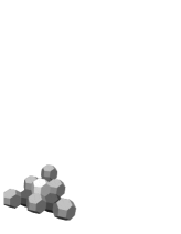
Let us comment the the choice of truncated octahedrons to represent atoms in the FIM model. We considered 3 possibilities: (i) point like atoms and the surface represented by triangles, (ii) hard sphere model, (iii) each atom represented by the truncated octahedron - the Wigner-Seitz cell of a bcc crystal structure. All these cases were preliminarily tested in simulations and we have chosen the representation by truncated octahedrons. The simplest representation by surface triangulation does not accurately reflect the atomic roughness of (111), (211) and (110) faces. The hard sphere model seems to be the best one, but it is difficult to use. If one takes the radius from the close-packed bcc structure, the surface contains plenty of holes between the spheres. On the other hand, choice of larger sphere radius leads to the reduction of the atomic roughness. Representation of atoms by truncated octahedrons ensures that the bcc crystal faces have proper symmetry and atomic roughness, and it is easy to use in numerical calculation.
II.2 Calculation of the electric field
To calculate the electric field distribution in the FIM model, first one has to solve Laplace’s equation (LE) in the space between the emitter and the screen Vurpillot et al. (2001, 2004).
| (1) |
where is the electric potential at the point r. It is assumed that at all points of the emiter surface and the at all points of the screen. Then the electric field is obtained:
| (2) |
To solve LE, Eq. (1), in the space between the emitter and the screen, finite element method (FEM) is applied, because it is well-suited for simulation of geometrically complicated domains O.C.Zienkiewicz et al. (2005); Rahman et al. (2006). All FEM related calculations are performed using Getfem++ package get , whereas tetrahedral meshes are generated using TetGen library tet . In our application of the finite element method the domain is divided into a number of tetrahedrons and Lagrange-type interpolation functions are used as the basic functions. For such mesh the electric field is constant in a tetrahedron. Hence, to assure appropriate accuracy of E, especially near the emitter surface, the linear size of a tetrahedron should be much smaller than the lattice constant . Direct computation does not allow for such mesh refinement, so we overcome this difficulty in the following way. First, we combine the numerical solution of LE with the analytical one. It follows from our preliminary calculation that at distances from the emitter greater than the electrostatic potential for the faceted emitter is practically the same as for the spherical emitter.
It is easy to show that the electrostatic potential for the spherical emitter is given by the formula
| (3) |
and applying Eq. (2) gives the electric field
| (4) |
A numerical solution of LE is limited to a subdomain of spherical shape with a radius . We apply Dirichlet boundary conditions to surfaces in with on internal (emitter) surface and on the external surface. In the space outside the , i.e., for distance , the analytical solution given by Eq. (3) and Eq. (4) will be used.
To obtain a numerical solution of LE in the subdomain with appropriate accuracy for FIM images simulation, we use 3-step procedure described below:
-
1.
The domain is divided into spherical layers – subdomains , , each with its own mesh of tetrahedrons. Then the LE is solved in the whole to get values of V on boundaries of each subdomain.
-
2.
In each subdomain the LE is solved again on a finer mesh of tetrahedrons applying Dirichlet boundary conditions to surfaces where the electric potential is known from solution obtained in the previous step.
-
3.
To calculate the electric field at a point r within :
-
(a)
A local subdomain is constructed by collecting all tetrahedrons with distance from r smaller than .
-
(b)
A new mesh is created by filling with newly generated tetrahedrons the space inside the boundary. There is a special, regular tetrahedron with center located at r
-
(c)
Using this mesh, LE is solved imposing V values from the boundary as Dirichlet condition.
-
(d)
Finally, the electric field is obtained as minus gradient of V calculated on
-
(a)
Typical technical data used in our calculation: the radius of emitter Å, assuming the lattice constant for tungsten: a=3.16 Å, the radius of domain , the radius of the screen , the number of subdomains , the number of tetrahedrons used in whole for the 1st step is and for the 2nd step in each subdomain , . The size of the special tetrahedron is in the vicinity of emitter surface. Hence, the ratio of to size of the special tetrahedron is over .
It is worth to emphasize an important role of the third step in our procedure of calculating the electric field by using a local subdomain . Omitting this step leads to an incorrect solution even in subdomain, although has the smallest linear size () and large number of tetrahedrons in its mesh .
We performed several tests to verify presented method of solving LE. The most important one concerned calculation of the electric field for an ideal spherical emitter because the analytical solution is known in this case – Eq. (4). The obtained numerical results are in good agreement with analytical solution. In the examined distance range up to , the relative error is smaller than and the deviation of direction from the radial direction is smaller then . We also obtained positive results for checking the symmetry of the electric field distribution on the different emitter shapes: pyramidal tip and bcc spherical one.
II.3 Calculation of the ion trajectories
Motion of an ion of mass M and charge q under the influence of force is described by the equation of motion
| (5) |
It is assumed that the ion is formed with zero initial velocity at a small distance () from a surface atom. It is convenient to express quantities occurring in Eq. (5) in reduced units. Choosing lattice constant as unit of length, as unit of E and as unit of time, the equation of motion Eq. (5) can be expressed in the form
| (6) |
where tilde denotes quantity in reduced unit. Thus, the trajectories in reduced units do not depend on the applied voltage, mass and charge of the ion. These quantities affect unit of time . To solve Eq. (6) we apply the velocity Verlet algorithm – commonly used in molecular dynamics simulationsFrenkel and Smith (1996), with a time step .
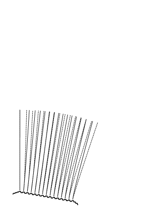
It is obvious that the direction of ion trajectory is not coincident with the electric field lines (see Fig. 2) even in the case of the initial ion velocity equal to zero. Due to the curvature of the electric field lines, instantaneous ion velocity at is deflected from up to large distances from the tip surface.
II.4 Calculation of a local magnification
Knowing the full ion trajectories we can investigate magnification not only on the distant microscope screen but also on virtual screens at small distances from the emitter. Analysis of FIM images on virtual screens is used to determine the minimal emitter – screen distance. Magnification is defined here as
| (7) |
where is the distance of a pair of points on the specimen and is the corresponding distance on the screen.
Another important quantity is the local magnification of distance defined as
| (8) |
where stands for average magnification. The average magnification can be replaced by magnification of a large distance, eg. the distance between ends of pyramid edges.
We found that local magnification of faceted crystal has a long-range dependence on the distance from the tip. Using the tip with curvature radius nm we obtained that the local magnification reaches of its final value at . At larger distances , , and . Hence, to control the error of , the screen –tip distance in the numerical model should be at least 30 times greater than the tip curvature radius, which is much greater than the distances used in previous numerical studies (see eg.Vurpillot et al. (2001, 2004)).
III Results and discussion
III.1 A perfect, single atom pyramid
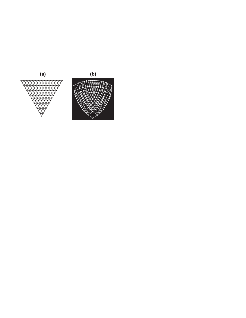
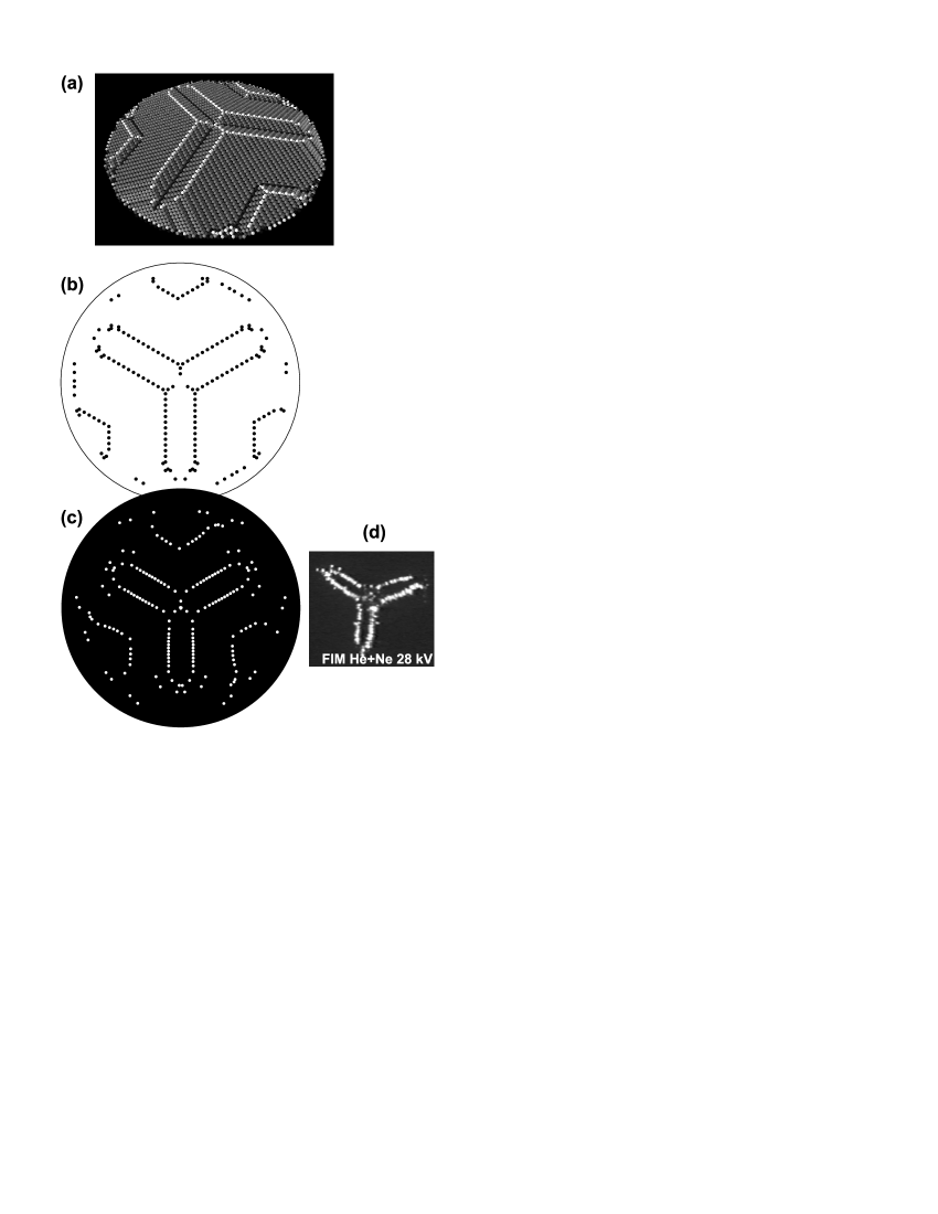
We begin our calculation with the simple case of a perfect 3-sided pyramid pointing in the [111] direction, formed by three densely packed crystal facets: (211), (121), (112). The crystallographic direction of the pyramid edges is . We assume that all atoms are in the BCC lattice positions and that the pyramid is ended by a single atom. This implies that that the number of atoms in the succcesive (111) planes is . The assumed sample configuration is shown in Fig. 3(a) and (b).
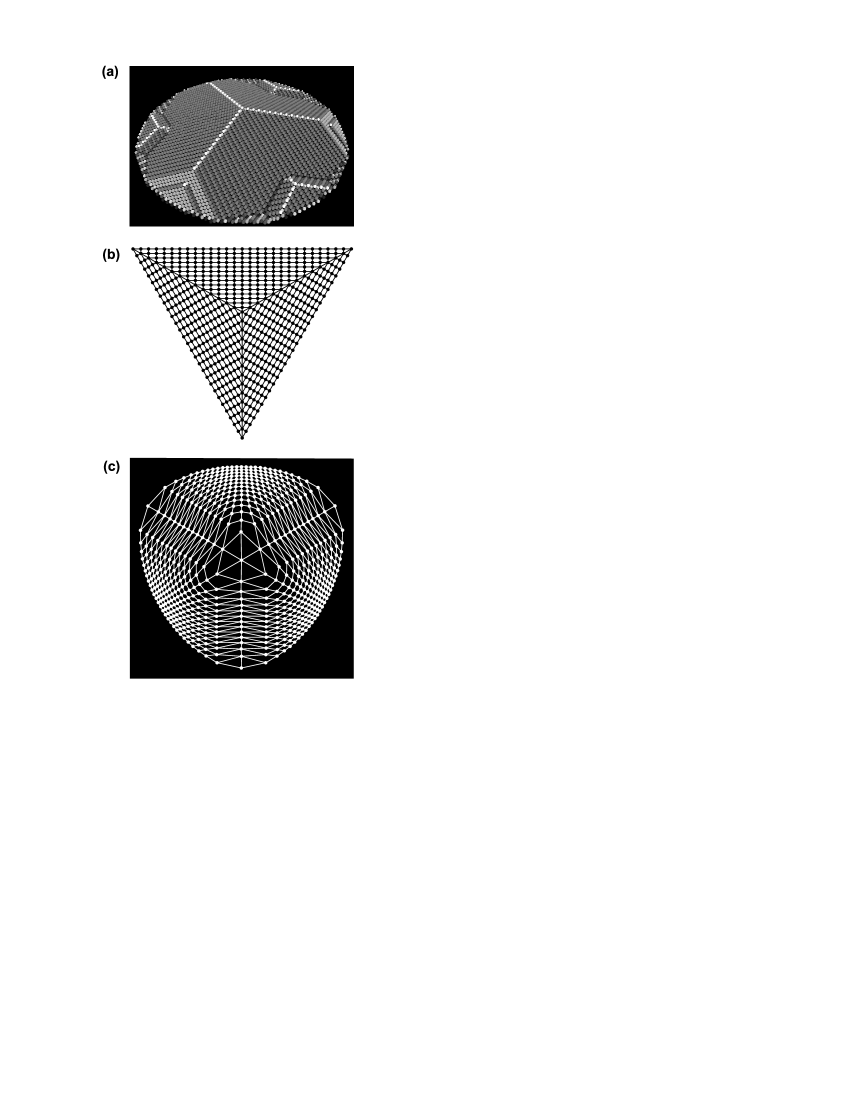
After calculating the resulting electric field between the sample and the microscope screen, we map the surface atoms onto the microscope screen by following the classical charged-particle trajectories (ions or electrons) – the solution of Eq. 5. The result is shown in Fig. 3(c). The calculated image shows some striking features.
- 1.
-
2.
The magnification of the image is highly inhomogenous. There is a great enhancement of the magnification at the apex of the pyramid. The local magnification factor at the apex is 4.5.
-
3.
Along the pyramid edge, the local parallel magnification varies from 2.8 near the apex, reaching a minimum (0.64) near the center of the edge (de-magnification), increasing to a value of 1.5 near the pyramid base.
-
4.
Along the pyramid edge, the local transverse magnification is 7.4 near the apex, quickly decreasing to a constant value of 6.7.
- 5.
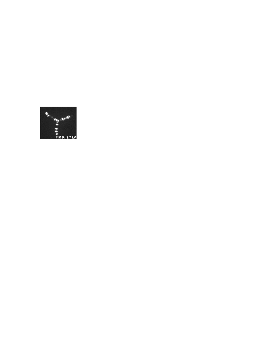
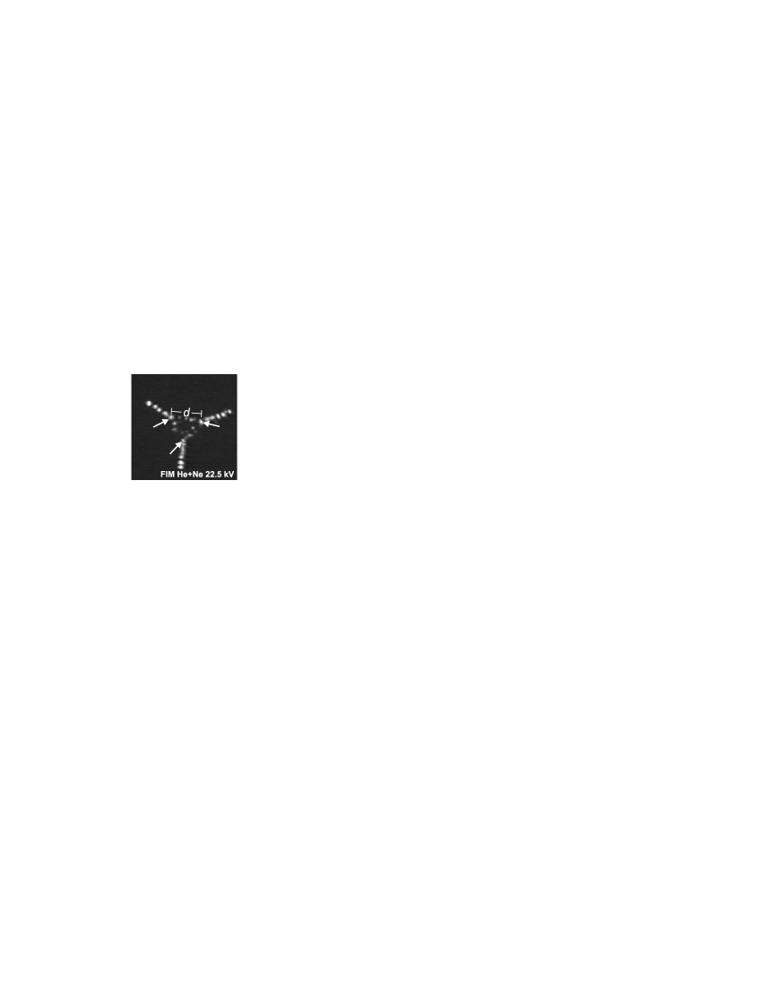
It would be very interesting to confront the above results with experiment. However, there is no easy way to calibrate an FIM image in terms of real distances. It is possible with careful FIM of samples with low average radii, where individual atoms are resolved, but as the average radius increases, the microscope resolution decreases and one looses the natural reference length of the lattice constant. However, observation 5. appears to explain a peculiar feature of FIM images of pyramids – the images of atoms at the edges are often not circular, but stretched in the direction perpendicular to the edges – see Fig. 4.
The image of atoms shown in Fig. 3(c) does not correspond directly to the experimentally observed FIM image, because in the real microscope only the most protruding atoms are visible. One of the reasons is that the protruding atoms, which can be thought of as “sharp” features on the otherwise smooth surface, cause local enhancement in the electric field. Imaging requires field ionization, which takes place for electric field magnitudes exceeding the ionization treshold. Experiments show that for the crystal shape considered here, only the edges of the pyramid are seen in the FIM image. For this reason, for the realistic simulation of the image, we select the atoms where the electric field above the atom exceeds a certain treshold [Fig. 5(a)]. In the last step we calculated the ion trajectories starting from the seletected atoms and extending up to the microscope screen to generate a simulated FIM image [Fig. 5(b)].

III.2 Truncated pyramids
The exact shape of the {211}-faceted crystal can be controlled by careful temperature treatment. It is possible to obtain pyramids with various degrees of vertex truncation or vertex rounding, which can be quantified by measuring the distance between the pyramid edge end pointsSzczepkowicz and Bryl (2005). However, such measurement in FIM suffers from errors caused by the inhomogenity of the local magnification. If one assumes constant magnification in FIM, the measurements of are always overestimated – that is, the pyramids are actually more “sharp” than they appear to be in the microscopic image. To calculate the correction for the measurements carried out in Szczepkowicz and Bryl (2005), we calculated a series of images of truncated pyramids. The height of the single atom pyramid was 14 geometrical atomic layers; now we remove 1,2,3 etc, obtaining an atomic configuration shown in Fig. 6.

Three examples of resulting images are shown in Fig. 7.
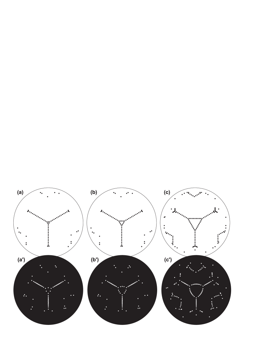
A striking feature is the shape deformation of the truncated vertex area, which has a triangular boundary on the assumed sample, but almost a circular boundary on the simulated image. In FIM experiments, the truncated area is not well resolved, but the boundary of the truncated vertex indeed often appears curved outword, as shown in Fig. 8.
As could be expected from the results presented in Sect. III.1, the local magnification in the central part of the image is high. For one atomic layer removed, the area of the truncated vertex increases 8.0 times; for 2 layers – 4.8 times; for 5 layers – 2.1 times. The corresponding linear magnifications, proportional to the square roots, are 2.8, 2.2 and 1.4, respectively. As the total height of the pyramid was 14 layers, the local magnifications calculated above correspond to height truncation of 7%, 14% and 36%.
Applying similar considerations as above to the magnification of the distance between the edge end points, it is possible to correct previous work on the dependence of the equilibrium crystal shape on the temperature Szczepkowicz and Bryl (2005), as shown in Fig. 9.
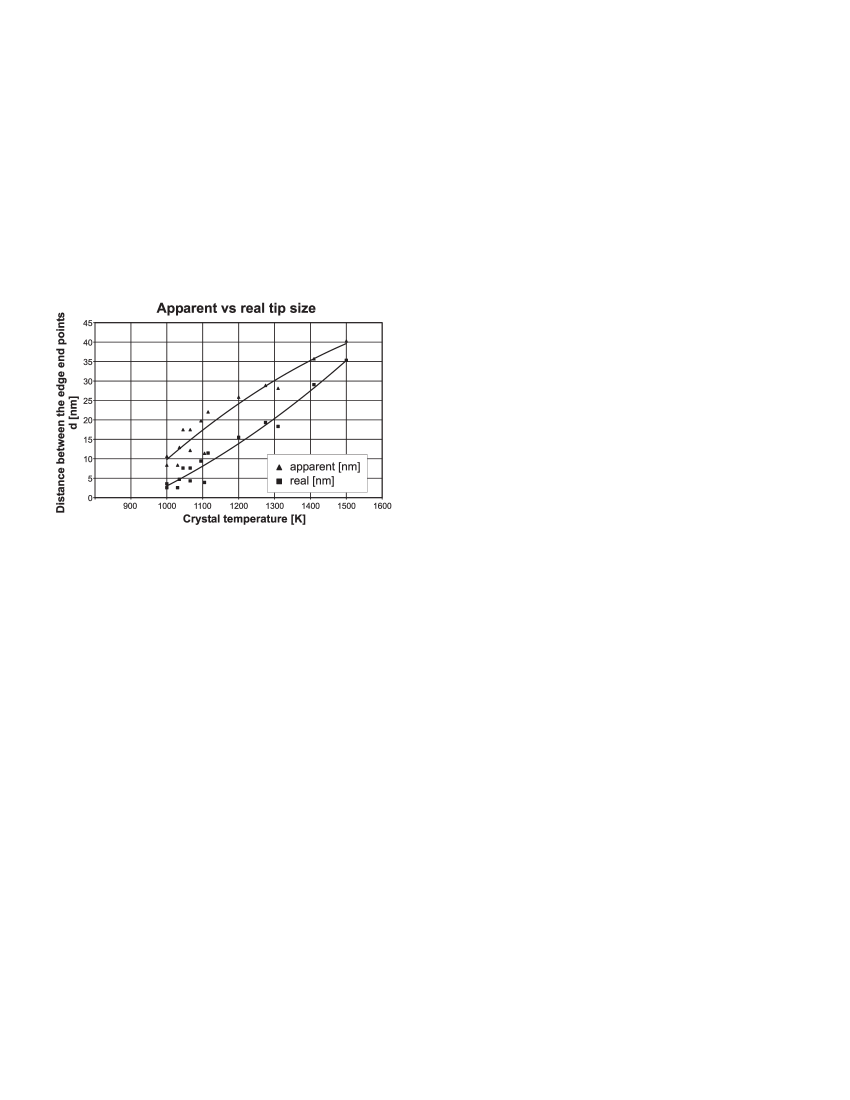
Note that without the correction based on this work, the amount of truncation of the pyramid is highly overestimated.
In Fig. 10 we demonstrate the simulated image of the (111) surface formed by truncating half of the height of the {211} pyramid.
In the experiment, at this pyramid size the indywidual atoms would not be resolved; however, in principle all the (111) lattice sites could be visualized using single atom adsorption on the (111) plane, similarly as in the work of Antczak and Ehrlich Antczak and Ehrlich (2005). In this way they have observed huge deformations of the image of an atomically flat crystal facet: curving of the atomic lines and an increase of the magnification near the boundary of the facet (Fig. 2 in Ref. Antczak and Ehrlich (2005)). Both of these features are present in the result of our simulation shown in Fig. 10, further confirming the validity of our model.
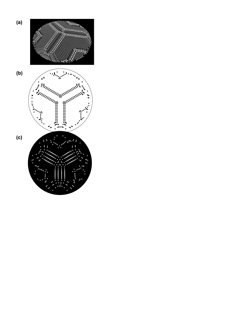
III.3 A steplike-faceted crystal (hill-and-valley faceting)
In the experiment, occurence of global faceting, where the shape of the faceted crystal is convex, such as described in Sect. III.1 and III.2, is only possible under special conditions: small crystal, high annealing temperature, and high desorption temperature of the adsorbate. If these conditions are not fulfilled, one obtains a steplike-faceted crystal Madey et al. (1999); Szczepkowicz et al. (2005). This is due to the kinetic limitations on the surface diffusion of the crystal material. For this reason we consider here a steplike-faceted sample, as shown in Fig. 11.
The assumed atomic configuration closely corresponds to surface topography observed in the experiments (see e.g. Ref.Szczepkowicz and Bryl (2004)).
Comparison of the simulated and real FIM image [Fig. 11(c) and (d)] shows an overall agreement, but also a discrepancy in one aspect. In the experiment, the six step edges are not pairwise parallel. One possible reason is that our model sample has a different topography than the real sample near the boundary of the faceted region. Another possibility is that the real atomic configuration is not as perfect as assumed in the calculation [Fig. 11(a)]. Note the high variation of the local magnification along the step edge in the simulated image. Unfortunately, this effect cannot be verified in the real image [Fig. 11(d)] due to the lack of single-atom resolution.
Another atomic configuration, which is interesting for comparison with experiment, is shown in Fig. 12.
This is significant for the case of palladium-induced faceting of tungsten Nien and Madey (1997); Szczepkowicz et al. (2005). In these experiments, palladium forms a pseudomorphic physical monolayer on the sample. The edges of pyramids/steps are truncated, with one atomic row removed, as shown in Fig. 12(a). Comparison of the actual atomic arrangement [Fig.12(b)] with the simulated FIM image at the microscope screen [Fig.12(c)] reveals a serious problem in the interpretation of the FIM image in such a case: it is very difficult to infer from the image on the screen [Fig.12(c)] the actual configuration of the atoms [Fig.12(b)]. The image observed on the screen is very misleading, suggesting the presence of three series of four almost equally-spaced parallel edges. This constituted a serious problem in the interpretation of the ion images of Pd/W faceting. Our present calculations finally fully confirm the interpretation of the ion images assumed in previous workSzczepkowicz and Ciszewski (2002); Szczepkowicz et al. (2005), illustrated here in Fig. 13.
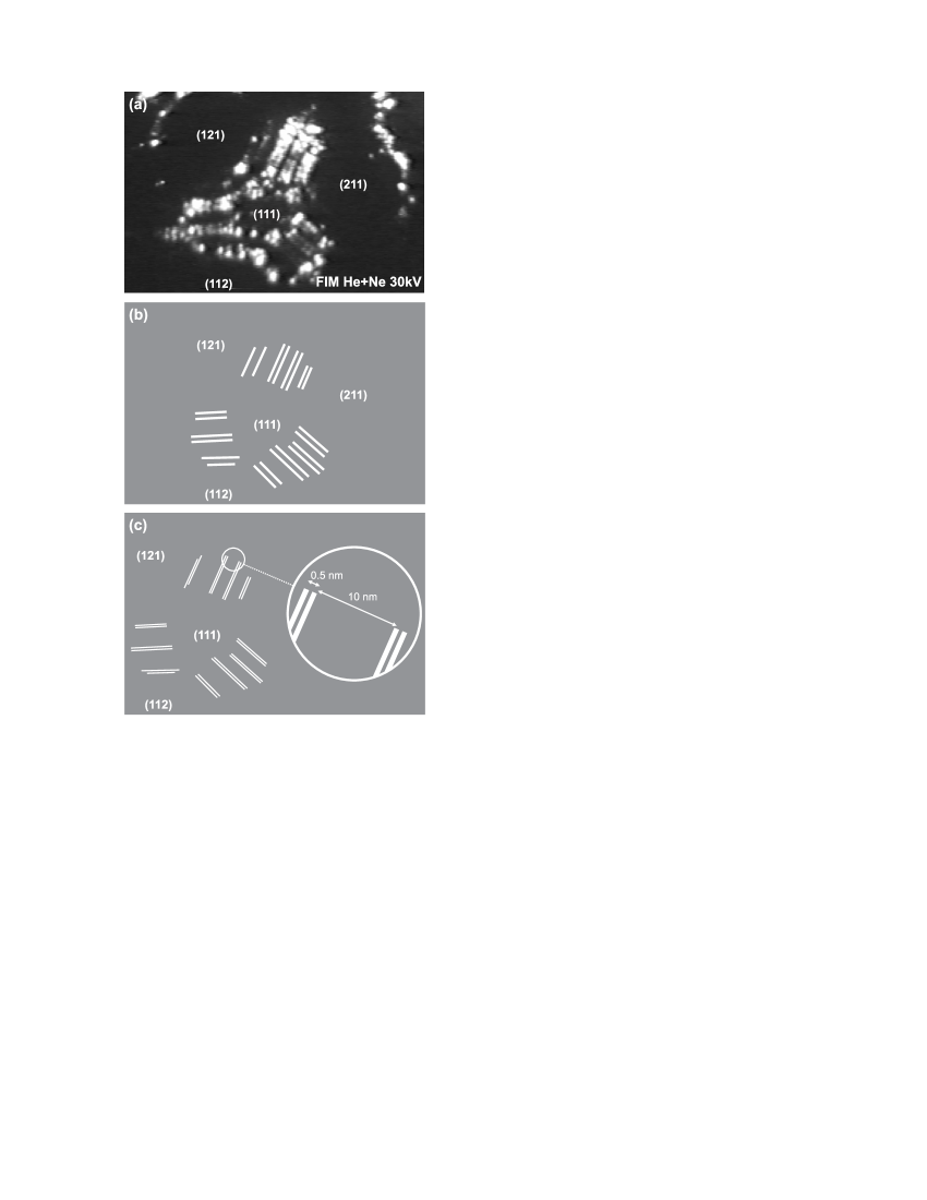
Calculations yield a very large magnification anisotropy: in the middle of the facet edges, the local transverse magnification is 3.1, while the local parallel magnification is 0.74. This results in the image magnification anisotropy of 4.2 at this point – the FIM image is stretched over 4 times in the direction transverse to the facet edges. In the experiment, the local transverse magnification is probably even larger, a rough estimate yields a factor of 7–8 (compare Fig. 13). However, this number is only an estimate, as there is no direct way to measure local magnification in the FIM experiment.
IV Conclusion
We performed detailed trajectory calculations in the FIM of {211}-faceted crystals (the case often encountered in research), and compared them with available experimental data. We found that the experimentally obtained FIM images of faceted crystals are often very misleading, and one has to rely on numerical calculations to fully account for huge local deformations of the microscopic image. Our main conclusions can be summarised as follows:
-
1.
In the consideration of faceted crystals, it is necessary for the model of FIM to take into account the atomic roughness of the tip surface and, at the same time, the large distance from the tip to the screen – the model must span many length scales. Our solution of Laplace’s equation demonstrates that the distance between the tip and the screen in the FIM model should be at least 30 times greater than the tip curvature radius in order to calculate the local magnification correctly.
-
2.
A combination of the finite element method with an analytical solution allows for accurate calculation of the electric field in the space between the tip and the screen.
-
3.
The FIM images of faceted crystals exhibit very large variations of the local magnification. We have found local magnification factors as high as 6.7 and as low as 0.64 (local de-magnification).
-
4.
As one moves along the pyramid or step edge, the parallel magnification varies by a factor of 2–4, reaching a minimum near the middle of an edge.
-
5.
The images of pyramid edges or step edges are exceedingly stretched in the direction perpendicular to the edge. The anisotropy of the local magnification, defined as the ratio of local magnification in two ortogonal directions, reaches a factor of 10 (for a perfect {211} pyramid).
-
6.
As a consequence of 5., an image of a truncated facet edge mimics the image of two distant parallel edges. Great caution is required in the interpretation of this kind of FIM images.
-
7.
The image of a single flat facet is distorted in such a way that the local magnification increases as one moves toward the facet edge. The atomic rows do not appear straight on the image. Although we have calculated only the case of a (111) facet on top of a {211}-pyramid, comparison with experiment suggests that this conclusion is generally true for isolated flat facets.
-
8.
Truncated {211} pyramids appear significantly more truncated in the FIM image than they are in reality; this effect is most pronounced for small truncations. Numerical calculations are necessary to estimate the size of a {211}-faceted tip.
References
- Tsong (1990) T. T. Tsong, Atom-probe field ion microscopy (Cambridge University Press, 1990).
- Miller et al. (1996) M. K. Miller, A. Cerezo, M. G. Hetherington, and G. D. W. Smith, Atom Probe Field Ion Microscopy (Clarendon Press, Oxford, 1996).
- Madey et al. (1999) T. E. Madey, C.-H. Nien, K. Pelhos, J. J. Kolodziej, I. M. Abdelrehim, and H.-S. Tao, Surf. Sci. 438, 191 (1999).
- Nien et al. (1999) C.-H. Nien, T. E. Madey, Y. W. Tai, T. C. Leung, J. G. Che, and C. T. Chan, Phys. Rev. B 59, 10335 (1999).
- Fu et al. (2001) T.-Y. Fu, L.-C. Cheng, C.-H. Nien, and T. T. Tsong, Phys. Rev. B 64, 113401 (2001).
- Lucier et al. (2005) A.-S. Lucier, H. Mortensen, Y. Sun, and P. Grütter, Phys. Rev. B 72, 235420 (2005).
- Rezeq et al. (2006) M. Rezeq, J. Pitters, and R. Wolkow, J. Chem. Phys. 124, 204716 (2006).
- Bryl and Szczepkowicz (2006) R. Bryl and A. Szczepkowicz, Appl. Surf. Sci. 252, 8526 (2006).
- Kuo et al. (2006) H.-S. Kuo, I.-S. Hwang, T.-Y. Fu, Y.-C. Lin, C.-C. Chang, and T. T. Tsong, Japanese Journal of Applied Physics 45, 8972 (2006).
- Fujita and Shimoyama (2008) S. Fujita and H. Shimoyama, Journal of Vacuum Science and Technology B 26, 738 (2008).
- Rahman et al. (2008) F. Rahman, J. Onoda, K. Imaizumi, and S. Mizuno, Surf. Sci. 602, 2128 (2008).
- Chang et al. (2009) C.-C. Chang, H.-S. Kuo, I.-S. Hwang, and T. T. Tsong, Nanotechnology 20, 115401 (2009).
- Kuo et al. (2008) H.-S. Kuo, I.-S. Hwang, T.-Y. Fu, Y.-H. Lu, C.-Y. Lin, and T. T. Tsong, Applied Physics Letters 92, 063106 (2008).
- Hommelhoff et al. (2006) P. Hommelhoff, Y. Sortais, A. Aghajani-Talesh, and M. A. Kasevich, Phys. Rev. Lett. 96, 077401 (2006).
- Hommelhoff et al. (2009) P. Hommelhoff, C. Kealhofer, A. Aghajani-Talesh, Y. R. P. Sortais, S. M. Foreman, and M. A. Kasevich, Ultramicroscopy 109, 423 (2009).
- Szczepkowicz and Ciszewski (2002) A. Szczepkowicz and A. Ciszewski, Surf. Sci. 515, 441 (2002).
- Szczepkowicz and Bryl (2004) A. Szczepkowicz and R. Bryl, Surf. Sci. Lett. 559, L169 (2004).
- Szczepkowicz et al. (2005) A. Szczepkowicz, A. Ciszewski, R. Bryl, C. Oleksy, C.-H. Nien, Q. Wu, and T. E. Madey, Surf. Sci. 599, 55 (2005).
- Szczepkowicz and Bryl (2005) A. Szczepkowicz and R. Bryl, Phys. Rev. B 71, 113416 (2005).
- Antczak and Ehrlich (2005) G. Antczak and G. Ehrlich, Phys. Rev. 71, 115422 (2005).
- Vurpillot et al. (2001) F. Vurpillot, A. Bostel, and D. Blavette, Ultramicroscopy 89, 137 (2001).
- Vurpillot et al. (2004) F. Vurpillot, A. Cerezo, D. Blavette, and D. Larson, Microsc. Microanal. 10, 384 (2004).
- Niewieczerzal and Oleksy (2006) D. Niewieczerzal and C. Oleksy, Surf. Sci. 600, 56 (2006).
- O.C.Zienkiewicz et al. (2005) O.C.Zienkiewicz, R.L.Taylor, and J.Z.Zhu, Finite Element Method: Its Basis and Fundamentals (Butterworth Heinemann, Burlington, 2005).
- Rahman et al. (2006) S. Rahman, J. Gorman, C. H. W. Barnes, D. A. Williams, and H. P. Langtangen, Phys. Rev. B 73, 233307 (2006).
- (26) Getfem++ home page: http://home.gna.org/getfem.
- (27) Tetgen home page: http://tetgen.berlios.de/.
- Frenkel and Smith (1996) D. Frenkel and B. Smith, Understanding Molecular Simulation (Academic Press, San Diego, 1996).
- Nien and Madey (1997) C.-H. Nien and T. E. Madey, Surf. Sci. Lett. 380, L527 (1997).