Optical Lattices for Atom Based Quantum Microscopy
Abstract
We describe new techniques in the construction of optical lattices to realize a coherent atom-based microscope, comprised of two atomic species used as target and probe atoms, each in an independently controlled optical lattice. Precise and dynamic translation of the lattices allows atoms to be brought into spatial overlap to induce atomic interactions. For this purpose, we have fabricated two highly stable, hexagonal optical lattices, with widely separted wavelengths but identical lattice constants using diffractive optics. The relative translational stability of 12 nm permits controlled interactions and even entanglement operations with high fidelity. Translation of the lattices is realized through a monolithic electro-optic modulator array, capable of moving the lattice smoothly over one lattice site in 11 s, or rapidly on the order of 100 ns.
pacs:
67.85.-d, 37.10.De, 03.67.LxI 1. Introduction
Optical lattices have provided a basis for numerous recent experiments with ultracold atoms, ranging from basic physics of single atoms in lattice potentials bloch_osc ; wsl , to interacting quantum gases bloch_mottins , and promises extension into quantum magnetism and exotic quantum phases OL_review . Particularly stimulating applications arise from the field of quantum information, where ultracold atoms in optical lattices are proposed to be good vehicles for the storage and processing of information Jaksch1999 ; Brennen1999 ; jaksch2000 ; jessen2004 ; daley2008 ; Bloch2008 ; KA2009 . Carefully engineered lattice potentials, even with dynamic modes of control, have become more common in modern quantum gas experiments Trotzky2007 ; Anderlini2007 . General methods for introducing additional degrees of freedom to periodic optical potentials to, for example, engineer the structure of a unit cell Lundblad2008 , or trap and manipulate multiple atomic species KA2009 are necessary to make further progress in these fields. Furthermore, the ability to probe and manipulate atomic information you2000 ; calarco04 ; shimizu04 ; STMcoldatoms ; Wurtz2009 ; Steinhauer09 ; lundblad09 with a spatial resolution well below the lattice spacing is of primary importance in these types of experiments nelson2007 ; Greiner09 .
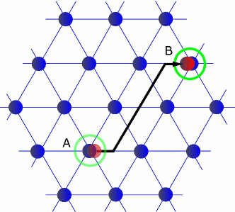
We describe the construction of an apparatus to achieve these aims using a new type of cold atom based microscopy, which we refer to as atomic quantum microscopy. This technique is a marriage of microscopy and quantum control, allowing the use of one quantum object to probe and manipulate a larger, more complex quantum system. Here, we employ two species of ultracold atoms, each confined near the minima of an optical lattice potential. The lattice wavelengths and intensities are chosen to ensure that each atomic species can be fully controlled by its respective lattice KA2009 . Through the combined use of controlled atomic collisions and spatial overlap of their wavefunctions, information concerning internal states and external degrees of freedom can be transferred from one species to the other, as illustrated in Fig. 1. This apparatus makes possible new types of measurements, such as probing the full quantum structure of complex many-body systems of interacting gases of atoms. Since the probe can be entangled with the sample, information can be read out in a way that does not interfere with the underlying more complicated quantum system, permitting idealized projective quantum measurements on a many-body system. In addition, entanglement between spatially separated portions of the sample can either be induced or interrogated. Application of this apparatus for scalable quantum information processing was described previously KA2009 , where a lattice potential at one wavelength confines qubit-atoms, and the probe atoms play the role of auxillary messengers mediating entanglement among (distant) qubits. Controlled interactions between species were proposed to entangle the internal states of atoms brought into close spatial contact.
We utilize novel techniques in the construction of optical lattices to produce commensurate lattice spacings with widely separated laser wavelengths, while providing precise differential control of the lattice site alignment through manipulation of optical phases. A relative translational stability of 12 nm is demonstrated. Based on previous quantitative analysis of a practical lattice configuration KA2009 , this yields an overlap fidelity of 99%.
In this article, we describe novel optical and opto-electronic components, including diffractive optical elements, aberration-balanced imaging, a monolithic array of electro-optic phase modulators, and the necessary driving electronics. These methods are applicable to both ultracold atom experiments exploring many-body physics and quantum information processing, where optical lattices with complex and/or dynamically manipulable unit cells are desired. The techniques may also be exploited in the manipulation of microscale objects of biological or other interest Grier2003 .
II 2. Commensurate, Multi-Chromatic Optical Lattices
Optical lattices are formed by overlapping two or more laser beams with wavenumbers on the atomic sample. When two beams intersect with an angle , they create a sinusoidal interference pattern with spatial frequencies , and phases determined by the relative optical phases of the beams. Here our goal is to construct bi- or multi-chromatic optical lattices with extreme relative phase stability and commensurate lattice constants for quantum microscopy. We achieve these goals by forming two lattices holographically, employing only common-mode optics.
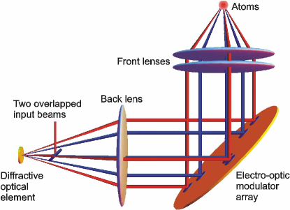
The optics for a hexagonal lattice are schematically shown in Fig. 2; this is the simplest two-dimensional geometry which is topologically stable against drifts in relative optical phases jessen96 . Two co-propagating beams with separated wavelengths and are incident on the two-dimensional reflective diffraction grating shown in Fig. 3, splitting each primarily into three first-order diffracted beams. After collimation by a lens, the diffracted beams pass through an electro-optic modulator (EOM) crystal (see Sec. 3), which imparts controlled phase differences between beams. They are then recombined and focused onto the atoms by a compound lens. The wavelength dependence of the diffraction angle at the diffractive optic naturally matches the angles of recombination, such that the resultant lattice geometries are identical in the absence of lens aberration (discussed in Sec. 2B). A separate one-dimensional lattice potential (not shown in the figure), applied along the optical axis and common to both atomic species, is used to complete the three-dimensional lattice potential.
II.1 A. Diffractive Optics
The central element in producing the bichromatic lattice above is the two-dimensional diffractive optical element (DOE) shown in Fig. 3, which imprints a patterned phase shift across the profile of the incident beam to create a two-dimensional diffraction pattern. The manufacture of intricate diffractive optical elements is a well established technique, typically accomplished with photographic emulsions, patterned metallic coatings, or photolithographed loewen ; wilson transmissive glass. We fabricated a reflective variant of a photolithographed DOE by first patterning a fused-silica substrate with reactive ion etching and subsequently coating the etched surface with a reflective gold layer.
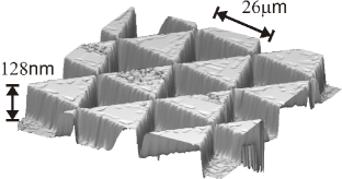
In order to efficiently diffract a single beam into three with the proper geometry, the element shown in Fig. 3 was designed. This grating can be modeled as three identical sawtooth-blazed line gratings, superposed with an angular separation of . This is equivalent to a two-dimensional array of alternatingly raised and recessed equilateral triangles, as shown in Fig. 3. The height separating raised and recessed plateaus reflects the line gratings’ blaze angles, determining the amplitude of each diffraction order. We etch to a depth corresponding to a half-wave phase shift, resulting in optimal extinction of the zeroth order. The size of the triangles determines the diffraction angle; for this experiment the side length is chosen to be 26 m, resulting in 1.7∘ and 2.7∘ for chosen as 681 nm and 1064 nm, respectively.
The grating pattern is transferred from a photoplotted chrome mask to a photoresist-coated fused silica surface and subsequently processed with reactive ion etching. Etching is performed with CF4 and O2 plasmas, repeated for the same pattern with multiple etch depths. Diffraction efficiency was optimized near the depth of 218 nm, one-quarter wave at the average of 681 nm and 1064 nm.
While the grating could function either in transmission or reflection, reflection is preferable as it eliminates etalon effects from second surface reflections, is better suited to withstand high laser powers, and eliminates dispersive effects in the substrate. After the grating is etched to the correct depth, the surface is coated with a 120 nm thick layer of gold using electron beam deposition (to aid in the adhesion of the gold film, a 5 nm thick layer of chromium is applied prior to the gold coating).
The performance and surface topography of the completed grating are assessed by optical measurements of diffraction efficiency and atomic force microscopy (AFM). This permits assessment of geometric distortions to the phase pattern, due to limited lithographic resolution and uniformity in etching and coating. The gratings direct approximately 10% of the incident light into each of the three first orders at the optimal wavelength.
With a beam diameter of 350 m, the diffraction efficiency remains unaffected until the incident laser power exceeds two watts. The damage threshold is found to be 4 kW/cm2, at which point we record a 5% permanent drop in the first order efficiency.
II.2 B. Abberation Cancelation
To construct optical lattices with significant atom tunneling, it is necessary to produce lattices with small site spacing and large beam intersection angles, requiring large numerical aperture optics. While sufficient control over aberrations at high numerical aperture is possible using aspheric imaging optics, simultaneous control over chromatic effects at large wavelength separations becomes technically challenging. This can be remedied in a straightforward way by canceling spherical aberrations with chromatic.
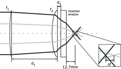
To form both lattices at the same distance along the optical axis, two front lenses (illustrated in Fig. 2) are necessary to correct for spherical and chromatic aberrations - we note that with a single spherical plano-convex lens, the separation between the two foci would be larger than a millimeter. This distance is the aggregate effect of longitudinal spherical aberration (LSA) and longitudinal chromatic aberration (LCA). The LSA is the distance between the axial intersection of a beam and the paraxial focus. The LCA, representing the axial distance between foci for the two wavelengths, has an opposite sign compared with LSA for normally dispersive lens media, presenting an opportunity to cancel their effects.
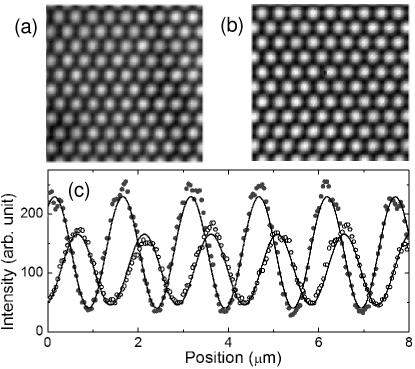

Our solution to this problem, without resorting to an arbitrary aspheric optical surface, is to use a standard aspheric lens (Asphericon GmbH, 50-40HPX-B) with focal length mm (50 mm diameter) and a weaker spherical lens with mm, as shown in Fig. 4. Without the weak lens, the system has little spherical aberration, and mm is negative because of the dominating chromatic aberration. The weak lens introduces enough spherical aberration to cancel the chromatic aberration, and shortens the overall focal length, resulting in a lattice constant of 1.5 m. The distance between the foci is reduced to 50 m, small enough to guarantee a good lattice overlap with beam diameters of 150 m and intersection angles of for 1064 nm and for 681 nm. The resulting lattice structures are shown in Fig. 5. The matching of lattice constants is also perturbed by aberration, resulting in a mismatch of 2%. Linecuts of the lattice intensity profiles are shown in Fig. 5(c). Here we have presented a simple lens design - to make further improvements to the lattice geometry, a multi-lens configuration can be designed to simultaneously match focus and preserve lattice constant matching.
For the quantum microscope, it is crucial to be able to introduce accurate spatial overlap of atomic wavepackets. The relative translational stability of the two lattices must be much smaller than the size of an atomic wavepacket, typically on order of 100 nm KA2009 . Mechanical instability of optical elements and mounts can cause an uncontrolled phase shift to individual beams, leading to a translation of the lattice through the unstable relative optical phase at the recombination point. Without exception, this optical setup consists of common-mode optics, implying that much of this motion is common to both lattices. This is necessary to achieve long-term relative stability. Fig. 6 shows a plot of the lattice position over time. Each lattice displays a stability of 60 nm on short time scales and drifts over 100 nm in 1500 s. This long-term drift cancels for differential motion, while vibration at audio frequencies is substantially suppressed. The root-mean-square relative translational motion is 12 nm, permitting high fidelity controlled atomic overlap greater than 99% KA2009 .
III 3. Translation of Lattice Sites
An essential element in atomic quantum microscopy is the ability to precisely address individual atoms by dynamically translating and overlapping lattice sites. For this, it is necessary to impart controlled phase shifts to the lattice beams. While there are several methods available for this, we have chosen electro-optic techniques to take advantage of high modulation bandwidths, and precise displacement without hysteresis. To preserve the stability provided by use of common-mode optics, the phase-shifting elements have been introduced in the form of a monolithic spatial light modulator formed by a single crystal of lithium niobate.
Two useful modes of lattice translation are possible for controlling atomic overlap. In the first, atoms are moved adiabatically over several lattice constants by slowly ramping the relative phase of beams with the EOM. The characteristic timescale for acceleration should then be matched to the vibration frequency for atoms on a lattice site, of order 10-100kHz. In the second, the lattice potential can be shifted rapidly enough by one lattice constant such that no atomic motion occurs. The combination of these modes allows essentially unlimited range of translation without vibrational excitation of the atoms. These two modes can be enabled through the use of a wide-range linear amplifier to drive the EOM, in combination with a fast switching technique to suddenly reset its output by a controlled amount.
III.1 A. Dynamic lattice translation
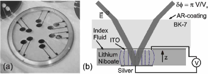
The EOM consists of six independent longitudinal modulators shown in Fig. 7(a), formed in a single crystal lithium-niobate wafer with multiple reflective silver electrodes on one side, and transparent, conductive indium-tin-oxide (ITO) pads on the other. The lithium niobate wafer is 75 mm in diameter, 3 mm thick, and has a -cut configuration (the optical axis is perpendicular to the wafer face.) One of the pads is shown schematically in Fig. 7(b). The silver electrodes were evaporated to a depth of 120 nm, doubling as mirror coatings, and allowing beams to propagate in a double-pass configuration. The ITO electrodes were evaporated to a thickness of 120 nm, serving not only as a transparent electrode, but simultaneously as a -wave matching (antireflective) coating near the mean wavelength between the indices of lithium-niobate and glass; a BK-7 window is then matched to the crystal with electrically nonconductive index fluid. The total front surface reflection is thereby reduced from the natural fresnel reflection between lithium-niobate and air of over 14% per surface to a reasonable 4% total loss. Stray reflections are subsequently blocked by apertures aligned to the main beams.

The half-wave voltage in a single-pass longitudinal modulator is given by , with the incident wavelength , the index of refraction for the ordinary ray and the electro-optic coefficient =8.6 pm/V lu . Since the electric field is parallel to the optical axis, and the polarization of the beams chosen to be perpendicular to the optical axis, only the coefficient need be considered. The half wave voltage, taking the double-pass and the incidence angle into account is =3.4 kV. To shift over one lattice site, one needs to apply twice the half wave voltage on one pad. In Fig. 8(a), we demonstrate a slow translation of the 681 nm lattice over 1.5 lattice sites with a differential swing of 10.4 kV across one pair of modulator pads. In Fig. 8(b), we demonstrate a fast jump of the lattice.
III.2 B. Modulator Electronics
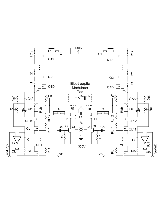
We use a pair of high voltage MOSFET ladder amplifiers to drive the two sides of each modulator pad (see Fig. 9). The design of the amplifier is similar to that described in Ref. HVAMP , modified to accommodate higher breakdown voltage MOSFETs (Ixys Corp., IXTY01N100), and to incorporate a triggered spark-gap as a switch. The upper limit in translational velocity of the lattice is determined by the slew rate of the amplifier, in turn determined by the total load and output capacitance, and available output current. Each EOM pad has a capacitance of 16 pF, a result of the necessary optical aperture, and high dielectric permittivity of the lithium niobate crystal. The amplifier is designed for modest power dissipation at a ladder voltage of 4.5 kV, resulting in a maximum output current of approximately 10 mA. This results in a modest slew-rate of 0.55 rad/s. While this is sufficient to provide adiabatic motion of atoms confined to the lattice, it is not sufficient to suddenly reset the amplifier diabatically for atomic motion. While higher amplifier currents might be provided by vacuum-tube based designs Holger , faster switching times are achievable augmenting the FET-based amplifier with semi-passive elements.
This can be accomplished using a triggered spark-gap to suddenly discharge the electro-optic capacitance as shown in Fig. 9 into the capacitor Cf. Since even a small capacitance spark gap is capable of conducting very large instantaneous currents, providing large standoff voltages, and reaching its conducting state quickly, it is ideally suited as a switch. In this case, the discharge of the electro-optic proceeds as an RC-waveform with time constant determined by the combined capacitance of electro-optic crystal, amplifier, and spark gap, and the total resistance, dominated by the surface resistivity of the electro-optic pad coatings. The most resistive element is the ITO coating; to minimize this resistance, a silver overcoat is evaporated on top of the ITO wires, resulting in a resistance smaller than . This, in principle, would result in a peak discharge current on order of 2 kA, with an exponential time constant on order 0.1 ns. In practice, however, we found this is limited to 10 ns timescales by the spark ignition process, which here is initiated by transformer coupling to an avalanche transistor trigger circuit. The switching amplitude can be controlled by the value of Cf.
IV 4. Conclusion
In summary, we have described the functional form of a quantum microscope for ultracold atoms based on atomic collisions and precisely controlled optical lattice potentials. We have presented all of the technical elements necessary to provide the controlled bichromatic lattice to manipulate ultracold atoms in the microscope, and demonstrated the necessary precision and dynamic control to implement a basic demonstration apparatus. Further improvements might be made by incorporating high-resolution optical microscopy of the potential in-situ, and using active feedback to further stabilize lattice overlap. Significant simplification of the apparatus might be possible by integration of the diffractive element with the optical phase modulator.
V Acknowledgements
The authors wish to thank Qiti Guo and Emily Garza for assistance in the production of the diffractive optical element. The authors acknowledge support from the NSF-MRSEC program under No. DMR-0820054, AFOSR/MURI Ultracold Molecules Program, and Packard foundation. N.G. acknowledges support from the Grainger Foundation. K.-A.B.S. acknowledges support from the Kadanoff-Rice MRSEC Fellowship.
References
- (1) M. Ben Dahan, E. Peik, J. Reichel, Y. Castin, and C. Salomon, Phys. Rev. Lett. 76, 4508 (1996).
- (2) S.R. Wilkinson, C.F. Bharucha, K.W. Madison, Q. Niu, and M.G. Raizen, Phys. Rev. Lett. 76, 4512 (1996).
- (3) M. Greiner, O. Mandel, T. Esslinger, T. W. Hansch, and I. Bloch, Nature 415, 39 (2002).
- (4) I. Bloch, J. Dalibard and W. Zwerger, Rev. Mod. Phys. 80, 885 (2008).
- (5) D. Jaksch, H.-J. Briegel, J. I. Cirac, C. W. Gardiner, and P. Zoller, Phys. Rev. Lett. 82, 1975 (1999).
- (6) G.K. Brennen, C. M. Caves, P.S. Jessen, and I. H. Deutsch, Phys. Rev. Lett. 82, 1060 (1999).
- (7) D. Jaksch, J. I. Cirac, P. Zoller, S. L. Rolston, R. Cote, and M. D. Lukin. Phys. Rev. Lett. 85, 2208 (2000).
- (8) P. S. Jessen, I. H. deutsch, and R. Stock. Quantum Information Processing 3, 91 (2004).
- (9) A. J. Daley, M. Boyd, Martin, J. Ye, and P. Zoller. Phys. Rev. Lett. 101, 170504 (2008).
- (10) I. Bloch, Nature 453, 1016 (2008).
- (11) K.-A. B. Soderberg, N. Gemelke, C. Chin, New Journal of Physics 11, 055022 (2009).
- (12) S. Trotzky, P. Cheinet, S. Fölling, M. Feld, U. Schnorrberger, A. M. Rey, A. Polkovnikov, E. A. Demler, M. D. Lukin, and I. Bloch, Nature 319, 5861 (2007).
- (13) M. Anderlini, P. J. Lee, B. L. Brown, J. Sebby-Strabley, W. D. Phillips, and J. V. Porto, Nature 448, 452 (2007).
- (14) N. Lundblad, P. J. Lee, I. B. Spielman, B. L. Brown, W. D. Phillips, and J. V. Porto, Phys. Rev. Lett. 100, 150401 (2008).
- (15) N. Lundblad, J. M. Obrecht, I. B. Spielman, and J. V. Porto, Nature Physics 5, 575 (2009).
- (16) C. Kollath, M. Köhl, and T. Giamarchi, PRA 76, 063602 (2007).
- (17) L. You and M. S. Chapman. Phys. Rev. A 62, 052302 (2000).
- (18) T. Calarco, U. Dorner, P. S. Julienne, C. J. Williams, and P. Zoller. Phys. Rev. A 70, 012306 (2004).
- (19) F. Shimizu. Japanese Journal of Applied Physics 43, 8376 (2004).
- (20) P. Würtz, T. Langen, T. Gericke, A. Koglbauer, and H. Ott, Phys. Rev. Lett. 103, 080404 (2009).
- (21) A. Itah, H. Veksler, O. Lahav, A. Blumkin, C. Moreno, C. Gordon, and J. Steinhauer, arxiv:0903.3282v1 (2009).
- (22) K. D. Nelson, X. Li, and D. S. Weiss. Nat Phys 3, 556 (2007).
- (23) W. S. Bakr, J. I. Gillen, A. Peng, S. Foelling, and M. Greiner, arxiv:0908.0174v1 (2009).
- (24) D. G. Grier, Nature 424, 810 (2003).
- (25) P. S. Jessen and I. H. Deutsch, Advances in Atomic, Molecular, and Optical Physics 37. Academic Press Cambridge, (1996).
- (26) G. B. Friedmann and H. S. Sandhu, American Journal of Physics 35, 629 (1967).
- (27) J.-M. Lu, Photonic Devices. Cambridge University Press, (2005).
- (28) S. Reynolds, Measurement Science and Technology 3, 283 (1992).
- (29) E. G. Loewen and E. Popov, Diffraction Gratings and Applications. CRC Press, (1997).
- (30) C. G. Willson and B. C. Trinque, Journal of Photopolymer Science and Technology 16, 621 (2003).
- (31) H. Müller, Rev. Sci. Instrum. 76, 084701, (2005).