A Fault Tolerant, Area Efficient Architecture
for Shor’s Factoring Algorithm
Abstract
We optimize the area and latency of Shor’s factoring while simultaneously improving fault tolerance through: (1) balancing the use of ancilla generators, (2) aggressive optimization of error correction, and (3) tuning the core adder circuits. Our custom CAD flow produces detailed layouts of the physical components and utilizes simulation to analyze circuits in terms of area, latency, and success probability. We introduce a metric, called ADCR, which is the probabilistic equivalent of the classic Area-Delay product. Our error correction optimization can reduce ADCR by an order of magnitude or more. Contrary to conventional wisdom, we show that the area of an optimized quantum circuit is not dominated exclusively by error correction. Further, our adder evaluation shows that quantum carry-lookahead adders (QCLA) beat ripple-carry adders in ADCR, despite being larger and more complex. We conclude with what we believe is one of most accurate estimates of the area and latency required for 1024-bit Shor’s factorization: 7659 mm2 for the smallest circuit and seconds for the fastest circuit.
1 Introduction
Quantum computing shows great potential to speed up difficult applications such as factorization [23] and quantum mechanical simulation [31]. Unfortunately, recent attempts to estimate the area required for such important applications have resulted in impractically large areas; for example, a large area dedicated to fault tolerance led to one estimated chip size on the order of [13] for a 1024-bit Shor’s factoring algorithm. In this paper, we show that these large areas result from an assumption that the underlying quantum data path is not specialized—essentially a uniform “sea-of-gates.”
Since Shor’s factorization is such an important application of quantum computing, we believe that it justifies significant effort to produce a practical, optimized circuit. This paper examines specialized circuits and layouts for Shor’s factorization, using an ASIC-like tool flow. Because error correction can easily dominate the area and latency of any quantum circuit, we must avoid excessive error correction operations by limiting movement, balancing resource usage, and selectively correcting for errors. Thus, we introduce a new composite metric for probabilistic circuits, called Area-Delay-to-Correct-Result (ADCR), which is a quantum equivalent of the classic Area-Delay product. ADCR permits quick comparisons of the efficiency to which quantum layouts make use of area. One surprising insight that results from careful accounting is that area devoted to error correction does not dominate the area of an optimized quantum circuit.
In tackling Shor’s factorization, we start with the structure of Shor’s algorithm, shown in Figure 1. Here, we see that quantum addition is fundamentally at the core, suggesting that an optimized adder circuit is important to efficient factoring. Consequently, we take a three-pronged approach:
Balanced Ancilla Generation:
We utilize shared ancilla factories [24, 17] to greatly reduce the area required for ancilla generation. Section 3 presents mapping heuristics that allow us map a quantum circuit to compute regions with shared ancilla generators while automatically segregating idle data bits to special memory regions with lower ancilla bandwidth. It finishes by provisioning a custom teleportation network to communicate over longer distances.
Aggressive Error Correction Optimization:
Since error rates in quantum computers are so high, most quantum computer architects have opted for a brute-force error correction strategy that corrects after every operation or movement. Section 4 shows how a more intelligent placement of error correction operations, modeled after circuit retiming, can reduce ADCR by an order of magnitude.
Tuning the Parallelism of Adder Circuits:
Since the quantum adder circuit [7, 28] is the core component to Shor’s factoring algorithm, Section 5 investigates microarchitectures and layouts for quantum adders. We believe that this is the first work to examine large quantum adder architectures in such detail.
At the core of this work is a custom computer aided design (CAD) flow for synthesizing fault-tolerant quantum layouts. We can accurately evaluate the area, latency and fault tolerance of circuits111Note that some of the partitioning heuristics that we describe in Section 3 are required to automatically evaluate organizations with specialized memory regions, such as CQLA [8]; previous evaluations were hand partitioned.. We can directly compare the efficiency of various quantum datapath organizations; Section 2 details these organizations and our evaluation methodologies.
Our investigation of Shor’s algorithm is very detailed (see Figure 21 in Section 6). Although it is hard to directly compare with existing proposals which contain many estimates (such as [13, 8]), we are confident that (1) our methodology provides one of the most realistic evaluations of area and latency for 1024-bit Shor’s factoring and (2) our layouts are an important step forward toward optimal factoring circuits.
2 Architectural Exploration
This section describes the quantum datapath organizations that we will use in other sections. It also introduces our CAD flow, error analysis, and evaluation metrics.
2.1 Abstracting Ion Trap Computers
We utilize Ion Trap technology [12] as the substrate for quantum datapaths. Table 1 shows basic error rates and latencies. It includes two “Error Sets,” one that we believe represents state of the art (Set 1) and one with a higher fault rate to explore error correction (Set 2). As described elsewhere [17, 30], our layout and simulation infrastructure utilizes an abstraction of Ion Traps, mentioned briefly here:
-
•
Qubits: Qubits (ions) are represented by their position in the substrate as well as fidelity (level of error).
-
•
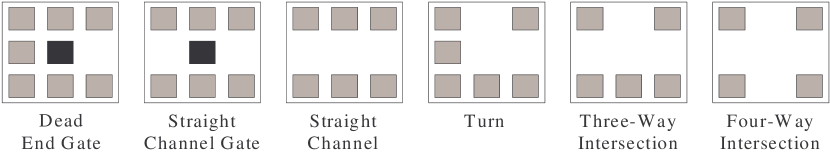
Layout: We utilize the macroblock abstraction, shown in Figure 2. Each macroblock has one or more “ports” through which qubits may enter and exit and which connect to adjacent macroblocks. To perform a gate operation, involved qubits must enter a valid gate location and remain there for the duration of the gate. A layout for a circuit consists of a tiling of macroblocks and a schedule for qubit movement and operations.
-
•
Movement: Trapped ions are moved via pulses applied to electrodes. Since ions are trapped, they can only move along channels specified by the layout.
-
•
Gates: Gates are performed by firing laser pulses at trapped ions. We abstract the physics and consider that a gate is performed after arrival of appropriate qubits at “gate locations” in the layout.
This representation provides sufficient accuracy to evaluate the area, latency, and error behavior of quantum circuits.
| Error | Error | Latency | |
| Physical Operation | Set 1 [10] | Set 2 [26] | in (s) [11] |
| One-Qubit Gate | 1 | ||
| Two-Qubit Gate | 10 | ||
| Measurement | 50 | ||
| Zero Prepare | 51 | ||
| Straight Move (30 m) | 1 | ||
| 90 Degree Turn | 10 | ||
| Idle (per s) | N/A |
![[Uncaptioned image]](/html/0909.2188/assets/x4.png)
| Datapath | Description |
|---|---|
| QLA | Original Quantum Logic Array [13], compute regions only, no specialization |
| LQLA | QLA with an optimized ancilla generator from [18] |
| CQLA | Compressed QLA [8], compute and memory regions specialization, original ancilla generator |
| CQLA+ | CQLA with a better performing ancilla generator from [25] |
| Qalypso | Our architecture [17]. Variable sized compute and memory regions, variable resources in ancilla generators and teleport network. “Pipelined” ancilla factory optimized from design in [25]. |
2.2 Quantum Datapath Organization
Proposed architectures for quantum computers have all consisted of computation regions connected by an interconnection network using quantum teleportation [13, 16]. High fault rates in quantum computing necessitate the widespread use of quantum error correction (QEC). Further, ancilla state generation is important to aid in the correction process [24] and as an integral part of quantum algorithms.
Three Major Organizations:
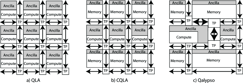
Figure 5 shows three major datapath organizations that represent the “state of the art” in quantum computing222Since circuits are mapped to these datapaths, they are not quite “architectures” but rather raw material for constructing architectures.. They are QLA [13], CQLA [8], and Qalypso [17] and can be viewed as a spectrum from inflexible to flexible ancilla distribution. They differ in their configuration of compute regions, ancilla generation areas, memory regions (for idle qubits), and teleportation network resources (for longer-distance communication)[16, 13].
The QLA architecture is most like a classical FPGA, in that all elements are identical: each element contains enough resources to perform a two-bit quantum gate. Each such compute region contain dedicated ancilla generation resources, space for two encoded quantum bits, and a dedicated teleportation router for communication.
CQLA improves upon QLA by allowing two different types of data regions: compute regions (identical to those in QLA) and memory regions (which store eight quantum bits) [8]. To account for different failure modes (idle errors vs interaction errors), data in memory regions are encoded differently from data in compute regions.
Finally, Qalypso improves upon CQLA by further relaxing the strict assignment of ancilla generation resources. It allows optimized, pipelined ancilla generators to feed regions of data bits (compute regions) that can perform more than just two-bit gates. The sizing of ancilla generators and data regions can be customized based on circuit requirements. Qalypso requires analysis (Section 3) to balance ancilla consumption with ancilla generation. Such analysis can automatically adjust the amount of ancilla bandwidth required in memory regions based on the residency time of qubits.
In all three organizations, each compute or memory region is placed adjacent to a teleport router. Qubits are moved ballistically within regions and teleported between regions.
Custom Component Design:
Proper design of the datapath elements (such teleportation routers or ancilla generators) is an important factor. In this paper, we pay careful attention to the teleportation network [16, 13]. We have produced layouts for the routers and EPR generators and utilize these in computing area, latency, and error probability of circuits. Sections 2.4 and 3.3 discusses how these numbers are derived and integrated with our evaluation methodology.
We also investigate a number of options for ancilla generation, as shown in Figure 5. The original QLA and CQLA papers used the ancilla generator shown in Figure 5a. Recent work by Kreger-Stickles and Oskin [18] showed that a layout such as Figure 5b, which is designed to minimize qubit movement and idling, is more fault tolerant and faster than the original QLA/CQLA ancilla factory under certain fault assumptions. We will insert this generator into the QLA datapath and refer to the result as LQLA. Finally, Figure 5c shows a more fault-tolerant variant of the original QLA/CQLA ancilla generator used in Qalypso [17]. It performs three copies of the QLA/CQLA generation process to produce a higher fidelity result.
An Organizational Zoo:
Figure 5 shows the datapath organizations that we will use in this paper. Three of these, namely QLA, CQLA, and Qalypso come directly from their original papers. LQLA is a variant of QLA utilizing the new ancilla generator and cell layout proposed by Kreger-Stickles. Finally, CQLA+ is a version of CQLA utilizing the improved ancilla generator from the Qalypso paper.
Evaluating such a disparate set of architectures is always challenging. When possible, we have adapted the exact qubit scheduling provided by authors (such as in LQLA, where the authors provided us with scheduling of qubits for their ancilla generator). To evaluate larger circuits, we have developed a hybrid evaluation methodology (described in Section 2.4) that permits us to stitch together modules.
We stray as little as possible from published organizations, with a few exceptions. First, our emulation of CQLA does not use a different ECC code between memory and compute regions. Second, assignment of qubits to memory regions happens automatically according to the mapping heuristics of Section 3, rather than through hand-partitioning. Third, LQLA is our invention, produced by inserting the optimal ancilla factory from [18] into QLA; this was necessary because the authors of [18] did not take a stand on long-distance communication or memory regions.
2.3 Synthesis of Application Specific Circuits
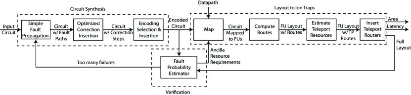
We have implemented a computer aided design (CAD) flow for quantum circuits. As shown in Figure 6, it consists of 3 main pieces: synthesis and optimization of error correction, mapping and layout of gates onto a substrate, and verification of fault tolerance properties.
Quantum circuits are specified in QASM, a quantum assembly language originally developed by Balensiefer et. al [2]. We have extended QASM with primitives that allow specification of control operations and better hierarchical design. One view of QASM is that it is a quantum netlist format, permitting the description of quantum circuits as a set of interconnected gates and scheduling constraints. Although some of the details of our CAD flow are prosaic, this flow is considerably more detailed, flexible, and complete than reported by other authors.
To map a QASM specification to one of the datapath organizations from Figure 5, we must map gate sequences to the compute and memory regions. Further, we determine the amount of ancilla necessary to perform error correction at each region and provision teleportation network resources to provide necessary bandwidth. Details of the mapping heuristics are presented in Section 3.
The error control mapping phase is one of the innovations of this paper. It takes a logical circuit, produces a redundantly encoded circuit in a specified quantum ECC code, then selectively adds error correction operations. We have developed a novel optimization procedure for slashing error correction overhead by a factor of three (3) over existing techniques from the literature, as discussed in Section 4.
2.4 Assessing the Error of Quantum Circuits
After a circuit has been mapped to one of the datapaths described in Section 2.2, we must evaluate the resulting error behavior. Circuits are typically large and hierarchically specified, leading us to develop a hybrid error modeling technique, described in this section.
As usual, we classify errors into three categories [2, 9]:
-
•
Gate: Errors that occur while manipulating quantum data. This category is the most widely studied in association with error correction performance. It is generally believed that gate errors will be the most significant of the three types.
-
•
Movement: Errors that result from moving quantum data. For example, ballistic ion movement in trapped ion technology involves accelerating and decelerating ions both linearly and around corners[14]. This induces unwanted vibrations or even collisions, disrupting the internal state that represents the datum.
-
•
Idle: Errors in idle qubits that result from spontaneous quantum effects. It is generally thought that idle or storage errors are the least severe of the three per unit time for most technologies.
In principle, we must simulate a circuit from start to finish, injecting errors by assuming that every gate, qubit movement, and qubit stall has an associated error rate and that every error event injects either a bit flip, phase flip or both. Unfortunately, interesting circuits are too large to do this exactly—leading to a need for a hybrid methodology.
| Data Regions | Memory Regions | Ancilla | Non-Trans | ||||||
|---|---|---|---|---|---|---|---|---|---|
| Datapath | Total | Qubits | Gens | Total | Qubits | Gens | Generator | Gates | Interconnect |
| QLA | 2 | 2 | none | [13] | anywhere | fixed-size routers, one per data/memory region | |||
| LQLA | 2 | 2 | none | [18] | anywhere | fixed-size routers, one per data/memory region | |||
| CQLA | 36 | 36 | 64 | 8 | [13, 8] | anywhere | fixed-size routers, one per data/memory region | ||
| CQLA+ | 36 | 36 | 96 | 12 | [17] | anywhere | fixed-size routers, one per data/memory region | ||
| Qalypso | [17] | placed with custom ancilla | variable sized routers adapted to design | ||||||
Hybrid Error Modeling:
Large designs are specified hierarchically, as a tree of modules. While we can synthesize a complete macroblock layout with fine-grained placement and routing for smaller modules, high-level modules are better handled via coarse-grained mapping techniques. Our mapper does not create exact macroblock specifications for all inter-block channels but instead relies on estimates of ballistic movement and teleportation based on inter-block distances. Further, the distance traveled from ancilla factories to data bits is estimated (quite accurately) after data bits have been placed. Consequently, we utilize a hybrid simulation model in computing communication costs and qubit idle times: not every qubit movement is simulated, but rather aggregate movements are computed and combined to speed simulation and support hierarchical design.
The calculation of the error probability for a mixed ballistic movement model involves three types of information: exact error probabilities, errors from estimated ballistic channels, and errors from teleportation channels. For smaller, leaf modules, we extract error properties exactly through simulation. The coarse-mapped distance estimates for longer ballistic communications are translated into a count of straight and turn macroblocks traversed, yielding error fidelity numbers for traversing these channels.
Finally, the effects of teleportation are determined by computing the fidelity and bandwidth of EPR bits in the channel. We have a model of EPR generation, routing, and purification which permits accurate computation of the latency to setup a teleportation channel as well as the fidelity of the EPR bits available for it. We compute the gate and movement errors within routers along the path, EPR generators, and purifiers. Section 3.3 gives more details.
Consequently, to compute the error probability of a large, hierarchically specified circuit, we combine inter-block movement and idle errors from ballistic and teleportation channels with the exact gate, movement, and idle errors in the compute and ancilla regions to produce one sequential list of possible error points in the layout as the circuit executes. This error list is passed to the Monte Carlo error simulator.
Monte Carlo Error Simulation:
To propagate errors, we utilize Monte Carlo (MC) simulation [25, 3], in which errors are sampled for each circuit element and errors are propagated accordingly. We traverse a graph representing the full circuit and layout, sampling gate, movement and idle errors (some of which are aggregate error counts for ballistic and teleportation-based communication) on each qubit in dataflow order. If the final state of the qubits results in an uncorrectable error, the run is counted as a failure. This process is repeated many times to get a statistically significant sample. Our tool uses the Colt JET library [1] version of the Mersenne Twister random number generator.
2.5 Evaluating Designs
In the following sections, we evaluate datapath organizations and layout heuristics via the following four metrics:
Area:
To measure the area of a quantum circuit, we first map that circuit to particular quantum datapath, then count the resulting number of macroblocks (see Section 2.1).
Latency:
The latency (Latency) of a quantum circuit represents the time to evaluate that circuit on a given layout. After mapping the circuit (including scheduling its operations), we measure the latency through simulation.
Success Probability:
The success probability () for a quantum circuit represents the probability that the result will be correct (error free) after evaluation. The success probability is measured with hybrid simulation (Section 2.4).
Area-Delay-to-Correct-Result (ADCR):
To evaluate the quality of quantum layouts, we propose a composite metric called Area-Delay-to-Correct-Result (ADCR). ADCR is the probabilistic equivalent of the Area-Delay product:
| ADCR | |||
For ADCR, lower is better. By incorporating potential for circuit failure, ADCR provides a useful metric to evaluate the area efficiency of probabilistic circuits. It highlights, for instance, layouts that use less area for the same latency and success probability. Or, layouts that use the same area for lower latency or higher success probability.
3 Mapping Circuits to Datapaths
In this section, we discuss the process of mapping a quantum circuit to one of the datapath organizations from Section 2.2. Table 2 details the various parameters that must be determined for each datapath organization. Many of these parameters are derived directly from papers by the various authors; only Qalypso provides complete flexibility in the number of Qubits () and Ancilla Generators () per data region as well as number of Qubits () and Ancilla Generators () per memory region.
3.1 Partitioning the Circuit
During the mapping process, the mapper must determine the total number of data regions () and memory regions () required. For QLA and LQLA, which makes it easy to determine as it is simply sized to accommodate the number of qubits used in the quantum circuit. The addition of memory regions introduces trade-offs in area and exploitable parallelism (latency). A datapath with a single compute region and a sea of memory can only perform one operation at a time — resulting in longer latency with a minimal area. A datapath such as QLA with all compute regions and no memory can exploit all possible parallelism in the circuit but with extremely high cost in area.
The mapper determines where each data qubit will reside during the course of the execution as well as when and where each quantum gate will execute. It starts with a coarse-grained partitioning of modules to compute-regions that minimizes communication. Next, the mapper attempts to schedule each gate operation so that it occurs as late as possible, while prioritizing operations on the critical path. The mapper relocates qubits into memory regions (if available) to free up compute regions for subsequent operations. As the mapper progresses, it tracks the location and times of all gate operations, error corrections, and network connections needed to perform the quantum circuit. The mapper discourages imbalanced mappings, such as those that over utilize network links or ancilla generation resources.
If the target datapath has fixed ancilla generation resources, the mapper attempts to map operations to regions with unused ancilla bandwidth. In datapaths with flexible ancilla generation (e.g., Qalypso), the mapper assumes that operations will never wait for ancilla, while still attempting to balance ancilla usage. A later phase (described below) matches ancilla generation resources to demand.
3.2 Ancilla Resources for Qalypso
Ancilla generation for four of the datapath organizations (i.e. QLA, LQLA, CQLA, and CQLA+) is fixed once an overall mapping has been determined. Qalypso, on the other hand, requires the mapper to calculate how many ancilla generation resources are needed at each compute and memory region. The amount of error correction performed is established in the synthesis phase of our flow (Figure 6) and used by the mapper. For memory regions, we compute the residency time for each qubit and use this to automatically add error correction steps when necessary; the residency calculation permits us to size the amount of ancilla generation () needed in each memory region.
Since it is impossible to perform all encoded gate operations transversally (i.e. as a simple function of the encoded bits) [32], we must provide for at least one non-transversal gate mapping. Non-transversal gates require special ancilla generators which are very time- and area-intensive; consequently, our mapper restricts operation of non-transversal basic gates to a limited number of locations.


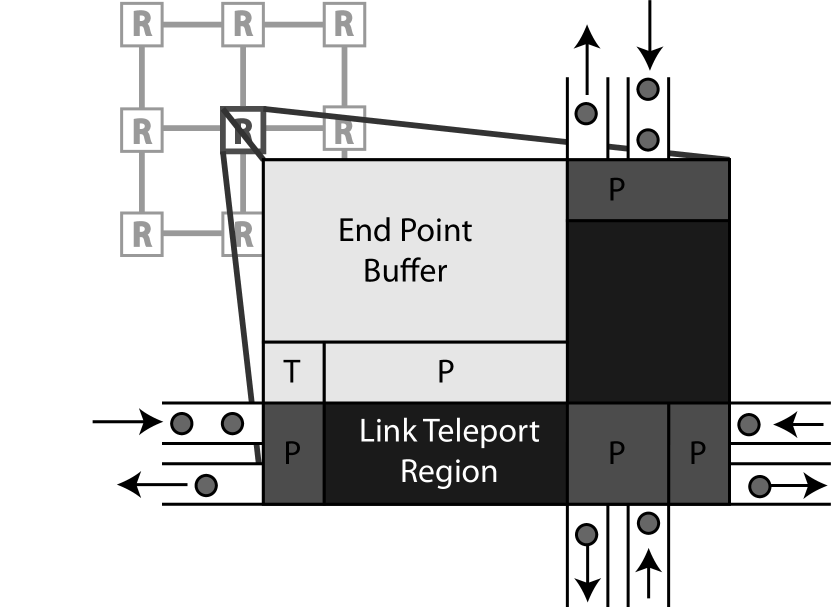
3.3 Network Resources for Qalypso
As mentioned earlier, teleportation is used to transport data over large distances (see [16, 13] for details). The time to set up a teleportation connection varies according to network congestion and routing choices. Ideally, a majority of the setup latency can be masked by the network, hiding all but the latency of a single teleportation operation from the data. In reality, congestion would limit the ability of dynamic scheduling hardware from realizing all of this benefit.
During the mapping phase, the mapper assumes all communication can be done without setup latency. This assumption is valid only if the network is sized appropriately. We size the network by tracking network consumption during mapping. Each requested network connection has an associated path consisting of the source router, intermediate routers, and destination router. The mapper tracks the load at each router (number of connections traversing and terminating at the router) for each time unit of the execution. When mapping is complete, this load information is used to determine the area of the router.333Note that the time component of teleport network usage distinguishes this channel sizing process from normal wire placement in an ASIC CAD flow. The area determined at this phase represents network resources required to run “at the speed of the data” [17]. We subsequently optimize area usage by retreating from this point; see Section 3.4.
A high-level floorplan of a network router is shown in Figure 7. The area of the router consists of purifiers (P) for EPR purification, teleporters (T) for connections that span multiple routers, and buffers to store qubits while waiting for the connection establishment. The area dedicated to each of these components is dependent on the maximum load the router sees, as determined by the mapping phase. Our tools cannot yet construct a detailed layout of arbitrarily sized routers. Instead, in an effort to obtain realistic network area estimates, we utilize a detailed layout of a specific sized router to extrapolate the sizes of larger routers.
3.4 ADCR-Optimal Layouts
Since the inherent parallelism and size of a circuit determines the need for data and memory regions, some aspect of the mapping process must select the total area available for mapping. Further, we need to adjust the aggressiveness with which the network is sized to meet transient communication demand. In principle, we would like to perform the mapping process with many different configurations, then select designs which meet some optimization metric. When the optimization metric is ADCR (Section 2.5), then we refer to the resulting circuits as ADCR-optimal. For the remainder of the paper, graphs which show ADCR should be considered to present ADCR-optimal data points.
3.5 Generating Random Circuits to Eliminate Datapath Organizations
In this section, we apply our mapping and partitioning techniques, described above, in order to narrow the candidate datapath organizations for later sections of the paper. One strategy for datapath elimination would be to map real benchmarks to different organizations and use the result to choose the most effective organizations. The problem with this approach is that it requires circuits that vary in size and complexity to produce a definitive result. Instead, we map circuits generated by a random circuit generator that can produce a variety of sizes and complexities automatically.
The circuit generator produces random gate networks consisting of 1 and 2 qubit gates. Each random graph is parametrized by a Rent’s exponent [5], which effectively determines the number of wires crossing recursive min-cut partitions of the gate network; a larger Rent’s exponent signifies a circuit with greater connectivity. While other works have discussed random gate network generation for classical circuits [4], the specific fan-in and fan-out requirements for quantum circuits preclude these solutions. Instead, we pick the number of gates and qubits desired, then, for each gate, randomly pick 1 or 2 qubits and place the gate at the end of the network. We generate many of these random networks and plot the results as a function of gate count.
Figure 8 shows the cumulative effects of our partitioning mechanisms, ancilla balancing and network resource sizing by plotting the composite ADCR metric (see Section 2.5) using Error Set 2 (Table 1) as a function of circuit size for random circuits. For larger circuits, we see that the QLA and CQLA datapath organizations are far less area-efficient than the others. Consequently, the remainder of the paper will focus on mapping to LQLA, CQLA+, and Qalypso.

4 Optimizing QEC
In this section, we tackle the misconception that quantum error correction should occur after every quantum gate [21]. In fact, the insertion of quantum error correction operations can actually serve to increase the probability of error if used indiscriminately. The reason for this phenomenon is that quantum error correction involves gate operations and data movement – each of which increase the probability of error – even as they work to suppress this error.
The goal of the QEC synthesis flow discussed in this section is to perform selective error correction, as originally suggested in [20]. This paper provides the first concrete method for selectively inserting error correction operations into an encoded quantum circuit. Through mapping, partitioning, layout, and error simulation, we evaluate the resulting circuits to show that we can vastly improve area and latency while improving error behavior.
4.1 Casting Error Correction as Retiming
The standard “brute force” error correction method, which adds an error correction step after every operation, is unnecessary in many circuits because not every qubit operation contributes the same amount of error: a qubit that interacts with many “dirty” qubits will accumulate errors much faster than a qubit that interacts with “clean” qubits. The crux of our technique is to estimate the critical error path, or the sequence of qubit interactions that introduces the most error into the circuit, in a fashion that is similar to the critical latency path through a circuit. We will focus error correction resources on these critical error paths.
Figure 9a illustrates the process of estimating the critical error path. It uses a simple, but effective model of a complicated error propagation process to estimate a parameter we refer to as the Error Distance (EDist). This model assumes that (1) each gate introduces one unit of error and (2) all qubits interacting within a gate acquire the maximum error value out of those qubits. In this simple model, the correction procedure resets the error counts of the corrected qubits to a base value (the correction process itself is noisy so it is not typically set to 0). We assume an error correction can only work if an incoming qubit’s error count is below some threshold.
The traditional brute force method, shown in Figure 9b, conservatively applies error correction after every gate to ensure that qubit errors do not propagate to other qubits. In our optimized process, shown in Figure 9c, we only add error correction steps after operations whose EDist value exceed a critical threshold (in the figure, the threshold is 3).
We have formulated this optimization problem as a case of circuit retiming [19] from the classical CAD literature. We choose where to insert correction steps by solving the Bellman-Ford-style circuit retiming problem described in [19]. More specifically, we use the OPT2 clock period minimization from [19] by replacing the clock period with the maximum, tolerable error count (expressed as a threshold value of EDist). We must make one modification to the algorithm: our initial network has no “registers” (error correction steps), so we must perform a binary search to determine the number of correction steps are needed to achieve a particular period/error count.
Additionally, there is no constraint on the distribution of correction steps as there is on synchronous registers in the retiming case. This give us much more freedom to distribute them. In fact, a valid optimized placement might mean a particular qubit does not get corrected at all, if it only goes through a few gates.
| Correction? | EDist | Output success | Operation count |
|---|---|---|---|
| Every gate | N/A | 0.987 | 3105611 |
| Optimized | 3 | 0.966 | 708811 |
| Optimized | 6 | 0.956 | 366411 |
| Optimized | 9 | 0.870 | 24011 |
| None | N/A | 0.65 | 1024 |
Table 3 illustrates why this error optimization seems so promising at first glance. It shows the results of optimizing an unmapped, 1000-bit random circuit using a variety of EDist values. We see that an optimized circuit can demonstrate little or no degradation in the probability of success for factors of 2 or 3 in operation reduction. Figure 10 shows that the probability of a mapped circuit actually improves under some circumstances with the optimization – even though the optimization is performed on the unmapped circuit.
By tuning the EDist threshold, we adjust the aggressiveness of the optimization. To do this automatically, we can perform a binary search over possible thresholds and pick (1) the count with the highest success probability, (2) the highest value that achieves a minimum success probability, or (3) the best success probability within a particular resource budget. While our simple EDist propagation model is useful while performing the optimization, it is important to evaluate the resulting circuits with a more accurate model — after mapping. Thus, one should iterate through the layout process as part of choosing an optimal EDist value.
4.2 Validation of Retiming Heuristic


For the remainder of the paper, we choose option (2), from above: perform a binary search to determine the value of the EDist parameter that yields no more than a 5% degradation in the probability of success on a mapped circuit (e.g., optimization along the X-axis of Figure 10).
Figure 11 presents the results of optimizing random circuits with Rent’s parameter r=0.5 on the three most promising datapath organizations from Section 3.5, using Error Set 2 (Table 1) for emphasis. This figure shows that the QEC optimization is quite successful in reducing ADCR on mapped circuits, showing up to a factor of 10 improvement in many cases. Section 5 shows that the optimization works even better on non-random circuits, such as adders.
4.3 Post-Mapping Adjustments
Our QEC optimization utilizes a simplistic gate error model during the placement of error correction operations. Since it effectively works on unmapped circuits, it does not currently adjust for other sources of error. Although the previous section showed that this technique performs quite well on mapped circuits, we could imagine that high movement and idle error rates or long channels in a large circuit could lead to a mapped circuit that behaves sub-optimally after optimization. Specifically, we expect to see two effects:
-
•
Degradation in fault tolerance as the gate error based optimization becomes less relevant due to relative increases in other error types.
-
•
Improvement in fault tolerance as reduction in error correction resources leads to more compact designs with shorter communication distances.
As future work, we anticipate reevaluating the error propagation of a circuit, once it has been mapped, and adjusting the mapped circuit through selective addition or removal of error correction operations. This post-mapping QEC adjustment will remove non-uniform error propagation introduced by the mapping process. Hopefully this step would lead to a higher probability of success.
![[Uncaptioned image]](/html/0909.2188/assets/x12.png)
![[Uncaptioned image]](/html/0909.2188/assets/x13.png)
![[Uncaptioned image]](/html/0909.2188/assets/x14.png)
![[Uncaptioned image]](/html/0909.2188/assets/x15.png)
5 Adder Microarchitectures
As discussed in Section 1, the quantum adder is a fundamental component of Shor’s factorization. Consequently, this section will apply the machinery that we developed in previous sections to produce optimized adder circuits. Since we are targeting 1024-bit factorization, we will examine 1024-bit adders. Further, for non-random circuits, we will switch to the more realistic Error Set 1 from Table 1.
5.1 Ripple-Carry vs Carry-Lookahead
We evaluate the quantum ripple-carry adder (QRCA) [6] and the quantum carry look-ahead adder (QCLA) [7], constructing larger adders from smaller adder modules, similar to what is done with classical bit-serial adders. Figure 15 shows how an -bit QRCA is constructed with multiple passes through a single -bit sub-adder. The registers can map to memory regions and the adder block to compute regions such that data is shuttled between memory and compute when it uses the sub-adder. Similarly, Figure 15 shows how an -bit QCLA is constructed with smaller modules. The modular approach allows us to trade area for parallelism thus allowing us to construct optimal adder configurations.
Figure 15 shows ADCR as a function of sub-adder size for both QRCA and QCLA architectures. This figure shows QEC-optimized circuits mapped to the three best datapath architectures. Interestingly, QCLA beats QRCA by a factor of 10 or 20 (for a given datapath organization). Since QCLA seems to be so much more area-efficient, we will concentrate the bulk of our analysis on QCLA.
![[Uncaptioned image]](/html/0909.2188/assets/x16.png)
![[Uncaptioned image]](/html/0909.2188/assets/x17.png)
5.2 Area for Quantum Error Correction
One of the more interesting issues that we can tackle with our CAD flow is to determine what fraction of an optimized circuit is devoted to quantum error correction. Some authors have contended that error correction is the dominant activity of a quantum computing circuit [26, 2, 8, 13].
Figure 15 belies this conclusion. It shows an area breakdown for ADCR-optimal circuits for both QRCA and QCLA, with and without the QEC optimization from Section 4. The only area truly devoted to error correction is the “QEC ancilla” (producing zero-ancilla for use in error correction). The memory area (“Memory”) accounts for the storage of bits, but not the zero-ancilla generation required for error suppression (which is included in the QEC ancilla category). Two crucial components often ignored by other authors are the area devoted to the teleportation network (“Network”) and the area devoted to T-ancilla (“T ancilla”). This latter category is required to perform non-transversal quantum gates and is present in many real circuits444Although one might argue that some fraction of the T-ancilla area is performing error correction as part of generating T-ancilla for LQLA and CQLA+, T-ancilla generation does not strictly require error correction..
We can glean several interesting results from Figure 15: First, the area devoted to error correction (QEC-ancilla) is only 20%-40% for optimized Qalypso designs (where ancilla generation can be effectively balanced). Second, the QEC optimization reduces the QEC-ancilla generation by almost half for Qalypso and the combined QEC-ancilla and T-ancilla generation by more than half for other datapaths.
It is interesting to compare area utilization with operation counts: for the QEC-optimized, Qalypso mapped, 1024-bit QCLA, we find that 70% of the total operations are devoted to QEC ancilla generation, but only 5% are devoted to error correction (interaction of ancilla with data). Thus, the pipelined ancilla factories are working at high utilization to feed the actual error correction operations, suggesting that raw operation count is not a particularly good metric for understanding the overhead of error correction.
5.3 Studying the QCLA Architecture
Section 5.1 showed that the QCLA architecture is the clear winner over QRCA in area-efficiency (ADCR). We will investigate this architecture a bit more in this section.
First, Figure 17 shows the effectiveness of the error correction optimization on the quantum carry look-ahead adders. We see that the QEC-optimization can be extremely effective—lowering ADCR by a factor of 46 for the optimal Qalypso design and 2 to 3 orders of magnitude for the other datapath organizations. These latter datapath organizations suffer from serialization on ancilla generation and see a great improvement in latency as a result of optimization.

Second, Section 3.4 discussed the need for varying the configurations considered by the mapper in order to find an optimal layout. Figures 17 and 18 show how important it is to perform parameter variation during layout: they show the sensitivity of the QCLA layout to the number of data regions given to the mapper. As can be seen by these figures, both success probability and latency are strongly impacted when the mapper is given too few data regions. Beyond a certain point however, the mapper is able to achieve high probability of success and low latency. The ADCR-optimization seeks to find the knee of the curve, namely the lowest area that achieves low latency and high probability of success.


6 1024-Bit Shor’s Factorization
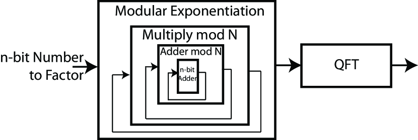
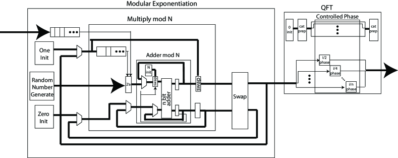
With Section 5 as a prelude, we are now ready to compute the latency and area of optimal Shor’s factoring circuits555Our failure probability simulation is not yet up to handling circuits of the size of Shor’s factoring; this is future work.. We will use the Qalypso datapath organization, since it has shown consistent advantage for both random circuits and adder circuits. Figure 21 shows a block-diagram of our target circuit. It consists of two main components: modular exponentiation and the quantum Fourier transform (QFT). For the modular exponentiation circuit, we rely on the work done in [28] and for the QFT, [15]. Since addition is a key component of the modular exponentiation circuit, we use our best adder designs from Section 5.
Our full, unoptimized implementation of Shor’s algorithm, including error correction, consists of physical operations. Our optimized version has 1000x fewer physical operations. The majority of the computation is dedicated to modular exponentiation (computing ); much less than 1% of the computation is spent on the QFT.
In Figure 21, we see that the QEC optimization yields a 55% improvement in latency for all circuit sizes using QCLA. Further, the difference in latency between factoring with QCLA and QRCA is about 40%. The fastest time for factoring 1024 bits is seconds, using a QCLA version of Shor’s. We note that this runtime is quite long; in the future, we hope to reduce this time with a more parallel implementation or further circuit optimizations.
Figure 21 shows area as a function of bits factored. One noticeable result is that the smallest area for 1024-bit factoring is 7659 mm2 using QRCA; this is more than 2 orders of magnitude smaller than previous estimates [13]. Another result is that the QEC optimization gives a 2.6x improvement in area for the QCLA version. The optimization nearly closes the area gap between QRCA and QCLA versions at 1024 bits (only a 13% difference). There are two possible causes for this: (1) we have not searched enough of the configuration space to pick the best QRCA design or (2) the primary error path in the QRCA (the long carry chain) offers only limited opportunities for optimization.
If we look at the breakdown in area, we see that the 1024-bit unoptimized QCLA-based design has 21% of its area dedicated to QEC-ancilla whereas the optimized version uses 12% of its area for QEC. Further, the QRCA-based design has about the QEC-ancilla area of the QCLA-based one.
7 Related Work
We are not the first to build a computer-aided design flow for quantum circuits. Balensiefer, et al. introduced one of the first complete frameworks for a quantum CAD flow [2]. Shende, et al., investigated logic optimization for quantum circuits [22]. Since we focus on reducing circuitry outside of the logical application circuit, our two approaches would be complementary. The concept of selective error correction was suggested by Oskin, et al. [20], although they did not provide guidance on how to perform these optimizations.
Draper pioneered the development of quantum adders [6, 7], while Van Meter and Itoh investigated the impact of communication and available concurrency on adder performance [27]. Our adder partitioning experiments work at a lower level, taking the logical adder structure as a given and determining physical geometries that perform best.
Using a teleportation network for long range communication was proposed in [20] and further exploited in [13, 8]. Our work provides the first systematic attempt to size router resources automatically based on circuit topology.
Although others have simulated error propagation in quantum circuits [25, 29, 3], we are the first to provide detailed error simulation for a modular design.
Finally, Shor’s factoring has been the focus of many studies. Some notable ones include [15, 13, 27]. In particular, Metodi, et al. [13] estimated design area for 1024-bit factoring at 0.9 , using a model of QLA. Our work advances the state of the art by applying more efficient resource allocation and significantly reducing the design area.
8 Conclusion
We examined quantum circuits by laying them out in a set of five different “datapath organizations”. We optimized the area and latency of Shor’s factoring while simultaneously improving fault tolerance through: (1) balancing the use of ancilla generators, (2) aggressive optimization of error correction, and (3) tuning the core adder circuits. In the process, we introduced a metric, called ADCR, which is the probabilistic equivalent of the classic Area-Delay product. ADCR provides a natural mechanism for optimizing layouts and subsequently evaluating area-efficiency—allowing us to eliminate two of the five datapath organizations immediately (QLA and CQLA), while leaving three others for further evaluation (LQLA, CQLA+, and Qalypso).
Our error correction optimization reduces ADCR by more than an order of magnitude, especially for less ancilla-efficient datapaths. Further, through a detailed analysis of optimized circuits, we showed that the area of a quantum circuit can have as little as 20% devoted exclusively to quantum error correction; this result belies conventional wisdom.
Finally, since quantum addition is at the heart of Shor’s factoring, we explored quantum adder architectures, showing that QCLA adders beat ripple-carry adders by a factor of 20 in ADCR, despite being larger and more complex. We concluded by mapping a complete Shor’s factoring circuit to show 7659 mm2 for the smallest circuit and seconds for the fastest circuit.
9 Acknowledgments
We would like to thank Mark Oskin and the reviewers for their helpful suggestions on improving the paper. Further, we would like to thank Lucas Kreger-Stickles for his help in understanding the ancilla generator used in LQLA.
References
- [1] Colt technical computing library in java.
- [2] S. Balensiefer, L. Kregor-Stickles, and M. Oskin. An evaluation framework and instruction set architecture for ion-trap based quantum micro-architectures. SIGARCH Comput. Archit. News, 33(2):186–196, 2005.
- [3] A.W. Cross, D.P. DiVincenzo, and B.M. Terhal. A comparative code study for quantum fault-tolerance. Arxiv preprint arXiv:0711.1556, 2007.
- [4] J. Darnauer and W.W.M. Dai. A method for generating random circuits and its application to routability measurement. In ACM Intl. Symp. on Field-Programmable Gate Arrays, 1996.
- [5] W.E. Donath. Wire length distribution for placements of computer logic. IBM Journal of Research and Development, 25(3):152–155, 1981.
- [6] T.G. Draper. Addition on a Quantum Computer. Arxiv preprint quant-ph/0008033, 2000.
- [7] T.G. Draper, S.A. Kutin, E.M. Rains, and K.M. Svore. A logarithmic-depth quantum carry-lookahead adder. Arxiv preprint quant-ph/0406142, 2004.
- [8] D.D. Thaker et al. Quantum Memory Hierarchies: Efficient Designs to Match Available Parallelism in Quantum Computing. Intl. Symp. on Computer Architecture, 2006.
- [9] K. Svore et al. Local fault-tolerant quantum computation. Phys. Rev. A, 72:022317, 2005.
- [10] M.J. Madsen et al. Planar ion trap geometry for microfabrication. Applied Phys. B: Lasers and Optics, 78:639 – 651, 2004.
- [11] R. Ozeri et al. Hyperfine Coherence in the Presence of Spontaneous Photon Scattering. Phys. Rev. Lett., 95:030403.
- [12] S. Seidelin et al. Microfabricated surface-electrode ion trap for scalable quantum information processing. Phys. Rev. Lett., 96(25):253003, 2006.
- [13] T.S. Metodi et al. A Quantum Logic Array Microarchitecture: Scalable Quantum Data Movement and Computation. Intl. Symp. on Microarchitecture, 2005.
- [14] W.K. Hensinger et al. T-junction ion trap array for two-dimensional ion shuttling, storage, and manipulation. Appl. Phys. Lett., 88:034101, 2006.
- [15] A.G. Fowler and L.C.L. Hollenberg. Scalability of Shor’s algorithm with a limited set of rotation gates. Phys. Rev. A, 70(3):32329, 2004.
- [16] N. Isailovic, Y. Patel, M. Whitney, and J. Kubiatowicz. Interconnection Networks for Scalable Quantum Computers. Intl. Symp. on Computer Architecture, 2006.
- [17] N. Isailovic, M. Whitney, Y. Patel, and J. Kubiatowicz. Running a quantum circuit at the speed of data. In Intl. Symp. on Computer Architecture, 2008.
- [18] L. Kreger-Stickles and M. Oskin. Microcoded Architectures for Ion-Tap Quantum Computers. In Intl. Symp. on Computer Architecture, 2008.
- [19] C.E. Leiserson, F.M. Rose, and J.B. Saxe. Optimizing synchronous circuitry by retiming. In 3rd Caltech Conference on VLSI, 1983.
- [20] M. Oskin, F.T. Chong, and I.L. Chuang. A practical architecture for reliable quantum computers. Computer, 35(1):79–87, 2002.
- [21] J. Preskill. Fault-tolerant quantum computation. Arxiv preprint quant-ph/9712048, 1997.
- [22] V.V. Shende, S.S. Bullock, and I.L. Markov. Synthesis of quantum-logic circuits. IEEE Transactions on Computer-Aided Design of Integrated Circuits and Systems, 25(6):1000–1010, 2006.
- [23] P.W. Shor. Scheme for reducing decoherence in quantum computer memory. Phys. Rev. A, 52(4):2493, 1995.
- [24] A.M. Steane. Space, Time, Parallelism and Noise Requirements for Reliable Quantum Computing. Quantum Computing: Where Do We Want to Go Tomorrow?, 1999.
- [25] A.M. Steane. Overhead and noise threshold of fault-tolerant quantum error correction. Phys. Rev. A, 68(4):42322, 2003.
- [26] A.M. Steane. How to build a 300 bit, 1 Gop quantum computer. Arxiv preprint quant-ph/0412165, 2004.
- [27] R. Van Meter and K.M. Itoh. Fast quantum modular exponentiation. Arxiv preprint quant-ph/0408006, 2004.
- [28] V. Vedral, A. Barenco, and A. Ekert. Quantum networks for elementary arithmetic operations. Phys. Rev. A, 54(1):147–153, 1996.
- [29] G.F. Viamontes, M. Rajagopalan, I.L. Markov, and J.P. Hayes. Gate-level simulation of quantum circuits. In Conf. on Asia South Pacific Design Automation, 2003.
- [30] M. Whitney, N. Isailovic, Y. Patel, and J. Kubiatowicz. Automated Generation of Layout and Control for Quantum Circuits. In Intl. Conf. on Computing Frontiers, 2007.
- [31] C. Zalka. Simulating quantum systems on a quantum computer. Mathematical, Physical and Engineering Sciences, 454(1969):313–322, 1998.
- [32] B. Zeng, A. Cross, and I.L. Chuang. Transversality versus Universality for Additive Quantum Codes. Arxiv preprint arXiv: 0706.1382, 2007.