Influence of the vacuum interface on the charge distribution in V2O3 thin films
Abstract
The electronic structure of V2O3 thin films is studied by means of the augmented spherical wave method as based on density functional theory and the local density approximation. We establish that effects of charge redistribution, induced by the vacuum interface, in such films are restricted to a very narrow surface layer of 15 Å thickness. As a consequence, charge redistribution can be ruled out as a source of the extraordinary thickness-dependence of the metal-insulator transition observed in V2O3 thin films of 100-1000 Å thickness.
pacs:
73.20.-r, 73.21.Ac, 73.61.-rI Introduction
Over the last decades, V2O3 has been investigated extensively by both experiment and theory – and still is a topic of great interest (see, e.g., Refs. rodolakis09 ; borghi09 and the literature given therein). Today, V2O3 thin films are receiving growing attention, particularly because the thin film geometry appears to strongly modify the electronic properties of the material as is most clearly demonstrated by the famous metal-insulator transition observed in bulk V2O3 as a function of temperature, pressure or doping imada98 . It is known that even a small alteration of the crystal structure, by Cr substitution kuwamoto80 or application of external pressure limelette03 , can have a serious effect on the metal-insulator transition in the bulk material. Therefore, it would not at all be surprising if structural modifications induced by the thin film geometry had similar severe implications.
Recently, the observation of a thickness-dependent metal-insulator transition in ultrathin V2O3 films was attributed to the increasing / lattice parameter ratio (decreasing , increasing ) because of interaction with the substrate luo04 . However, this conjecture has been refuted by both x-ray diffraction studies for high quality films grygiel07 ; allimi08 and density functional calculations sfe . In fact, the experiments point to a very complex thickness-dependence of the lattice parameters with unsystematic changes of the lattice constant for film thicknesses of 100–1000 Å, thereby calling for a more in-depth study of the electronic properties of these films. Indeed, in other systems, like the LaAlO3/SrTiO3 heterostructure CPL467 , it has been shown that interfaces can seriously modify the electron density profile. A strong dependence of the electronic properties on the layer thickness has been also reported for the hexagonal layer compounds such as klein2001 . In the present case a systematic investigation is still missing.
In this paper, we aim at clarifying the influence of the vacuum interface on the electronic states of V2O3 thin films. At this interface, two possible scenarii may cause a significant reorganization of the electronic states: (1) a local modification of the crystal structure and (2) a charge redistribution due to the broken symmetry at the vacuum interface. In general, charge redistribution due to a surface, similar to heterointerfaces, may induce a considerable deviation from the bulk properties, see, e.g., Refs. surf2 ; cpl449 ; gemming06 ; epl08 . Even though possibility (2) therefore seems to be promising, it is the aim of this paper to point at the limitations of such a mechanism for film thicknesses exceeding some 15 Å.
II Computational Method and Technical details
The calculations are based on density-functional theory and the local density approximation (LDA). They were performed using the scalar-relativistic implementation of the standard augmented spherical wave (ASW) method (see Ref. aswrev, , Chap. 2 of Ref. aswbook, and references therein). In the ASW method, the wave function is expanded in atom-centered augmented spherical waves, which are Hankel functions and numerical solutions of Schrödinger’s equation, respectively, outside and inside the so-called augmentation spheres. In order to optimize the basis set, additional augmented spherical waves were placed at carefully selected interstitial sites. The choice of these sites as well as the augmentation radii were automatically determined using the sphere-geometry optimization algorithm sgo . Self-consistency was achieved by a highly efficient algorithm for convergence acceleration mixpap . The Brillouin zone integrations were performed using the linear tetrahedron method with an increasing number of k-points in order to check the convergence with respect to the granularity of the k-point grid bloechl94 ; aswbook .
The V2O3 surface was simulated by means of a fivefold superstructure of the canonical hexagonal unit cell. The latter comprises six formula units, i.e. six V layers along the (hexagonal) axis. These layers are separated by O layers, giving rise to VO6 octahedra. For further details see, e.g., Refs. us0304 ; eyert05b and the references therein. The lattice constants and fractional coordinates of the atoms were taken from Ref. dernier70 . The surface was then generated by removing all atoms from one of the five hexagonal unit cells, see Fig. 1, such that one of the resulting surfaces terminates with an O layer.
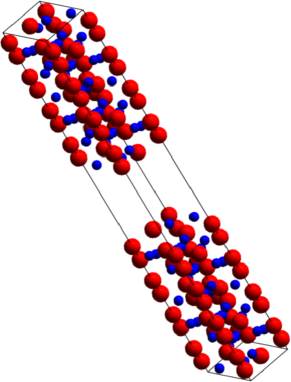
This vacuum interface is the subject of the subsequent discussion.
In order to separate the charge redistribution due to the broken crystal symmetry and the changes in chemical bonding at the vacuum interface from the structural relaxation effects at the V2O3 surface we will not include the latter in our considerations. In fact, structural relaxation is restricted to a very narrow range of about five atomic layers as has been pointed out in a detailed study by Kresse et al. kresse04 , which also provides an elaborate overview over the relevant literature. In contrast, we shall focus on the question whether the charge redistribution coming with the removal of bonding partners could affect the behavior of a much thicker slab of several 100–1000 Å. Consequently, accounting for the near-surface structural modification is, on the one side, dispensable and, on the other side, disadvantageous for a systematic analysis of the decay of charge redistribution effects.
Of course, in view of the strong electronic correlations present in , calculations beyond the standard LDA seem necessary. Indeed, while LDA fails to capture the metal-insulator transition of the bulk material, the latter could be successfully described using LDA+DMFT held01 ; keller04 . However, for the large supercell used in the present simulation of the surface the rather complex LDA+DMFT calculations would be beyond present day computational facilities. Even more important, the previous LDA+DMFT studies revealed that the strong electronic correlations come into play via the narrowing of the bands as calculated within the LDA, which occurs on going from the crystal structure of the metal to that of the insulator. Hence, there is a clear signature already in the LDA bands indicating the metal-insulator transition. As a consequence, although LDA has turned out to be insufficient in describing the metal-insulator transition itself, it clearly signals its occurrence. For that reason, it is well justified to omit a full LDA+DMFT treatment as long as the LDA results are carefully interpreted.
III Results
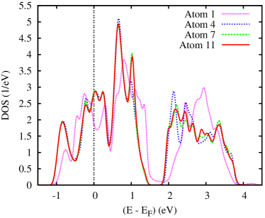
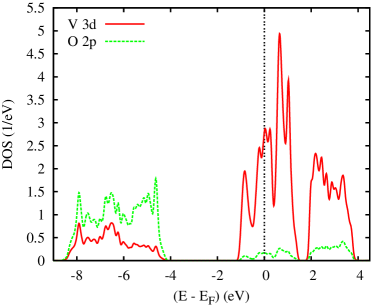
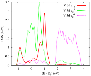
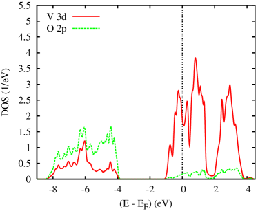
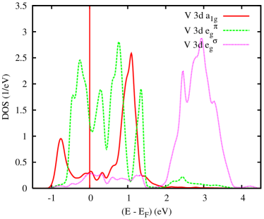


Due to the octahedral O-coordination of the V atoms in V2O3, the V electronic bands (located around the Fermi level) are subject to a splitting in two subgroups. While the partially occupied t2g manifold is found in the energy range from eV to 1.4 eV, the unoccupied states extend from eV to 3.7 eV. These two groups are clearly observed in Fig. 2, which depicts the site-projected V density of states (DOS) as obtained for various atoms in the thin film. Atoms are numbered according to their distance from the surface with atom 1 being located directly at the surface. We find that the shapes of the curves in Fig. 2 are closely related to each other. Only for atom 1, which is subject to the strongest interface effects, deviations are visible since half of the bonding partners are missing and the V–O therefore is reduced. In fact, the DOS curves of atoms 7 and 11, which are separated from the surface by about 18 Å and 28 Å, respectively, virtually resemble the bulk DOS shape. For this reason, the decay of the interface-induced relaxation of the electronic states is found to be very fast.
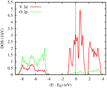
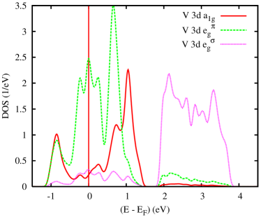
In order to establish further insight into the above-mentioned decay, we display in Fig. 3 V and O partial DOSs in a wider energy range in the left column as well as orbital resolved V partial DOSs in the right column. The nearly perfect splitting of the t2g manifold into and sub-groups traces back to the trigonal symmetry of the corundum lattice held01 . The partial DOS of V2O3 bulk (top row of Fig. 3) is almost identical to that found for a VO6 octahedron in the thin film some 28 Å beneath the surface (center row of Fig. 3). This holds for both the O and the V states. In contrast, the surface VO6 octahedron clearly shows distinct electronic relaxation effects of the local electronic states (bottom row of Fig. 3), which can be attributed to the modified chemical - bonding at the surface. In particular, for those V and O atoms, which miss a bonding partner due to the surface, we observe a reduction of the and occupation, respectively, of approximately 0.08 electrons. We point out again that in obtaining these results we did not take into account the V2O3 surface relaxation in order to distinguish between the electronic changes and the short-range structural distortions. Our results entail that the effect of the vacuum interface on the local electronic states, as reflected by the site-projected DOS, vanishes at about 15 Å below the surface. Charge redistribution induced by the surface is therefore restricted to the same narrow surface layer, in which the structural relaxation is observed kresse04 .
In a next step we turn to the discussion of -resolved quantities and display the electronic bands in Fig. 4. The top row of Fig. 4 depicts the band structure of bulk V2O3 as well as the non-primitive hexagonal Brillouin zone of the corundum lattice of V2O3, which here and in the following is used for representing findings of band structure calculations. The bulk results serve as a reference for comparison with the surface results given in the bottom left panel of Fig. 4.
Of course, the surface band structure comprises a lot more bands due to the simulation of the surface by the fivefold supercell of the surface slab as mentioned above. In this supercell, the increased number of different bands reflects the larger number of inequivalent atomic sites. V (and O) atoms with different distances to the vacuum are no longer equivalent from the crystallographic point of view. Furthermore, the dispersion along the high symmetry line –A is strongly suppressed due to the fact that this line corresponds to the direction perpendicular to the surface. Note that the construction of the surface slab in a fivefold supercell of the hexagonal V2O3 cell implies that the length of the line –A is reduced to a fifth and that the electronic bands are folded back. In order to enable a straightforward comparison with the bulk data, the line -A is thus artificially stretched to the original length in the slab band structure. Having this fact in mind, we eventually find that the surface slab reproduces the characteristics of the bulk V2O3 bands. In particular, there is no sign of an additional state, not present in the bulk, which could be responsible for the anomalous behavior of thin films.
It has been found for V2O3 thin films, that the and constants of the corundum lattice deviate slightly, i.e. less than 1%, from their bulk values grygiel07 ; allimi08 . In addition, we have shown that the influence of the parameter change on the electronic structure is negligible sfe . Here, we investigate whether modifications of the parameter may play a more important role by performing a surface slab calculation with the constant increased by 1% as compared to the bulk. The results are depicted in the bottom right panel of Fig. 4, which uses the same representation as before. Comparison with the bottom left panel of Fig. 4 shows that an elongation of the axis does not lead to a qualitative change of the electronic states. The two band structures are, in fact, almost identical. Hence, we obtain that the experimentally observed alterations of the V2O3 lattice parameters in a thin film influence the electronic states only marginally, as long as they are not accompanied by a relaxation of the atomic positions. Indeed, a substantial lattice relaxation has been advocated to interpret transport measurements grygiel08b .
To ensure that the thin film electronic structure fully resembles the bulk a final step is necessary. We still have to exclude differences in the contribution of the atomic orbitals to the different electronic states, since they would point at a modified chemical bonding. Orbitally weighted band structures are useful tools to address this question. Fig. 5

gives an example of a prototypical V atom, some 28 Å below the surface. Very similar results are obtained for the neighboring V sites. In Fig. 5, the bars added to each state have a length proportional to the contribution of the orbitals of the atom under consideration. States with minor admixture are not depicted for clarity. For this reason, some of the bands shown in the bottom left panel of Fig. 4 are missing in Fig. 5. We observe that the selected V site contributes to the bands in the entire energy range from eV to 1.4 eV and thus perfectly reflects the behavior of a bulk atom, which is true for any atom located at least 15 Å below the surface. Charge redistribution as induced by the vacuum interface therefore has to be excluded as a possible source for the novel electronic properties of V2O3 thin films. We finally mention that in the case of a heterosystems, like LaAlO3/SrTiO3 pentcheva08 ; lao , different charge redistributions have been obtained in LDA and LDA+U calculations. However, for the present system we do not find such a dependence.
In conclusion, our findings entail that neither the observed changes of the and lattice parameters in V2O3 thin films nor the response of the electronic system to the presence of the vacuum interface can explain significant deviations from the electronic properties of bulk V2O3. Only next to the surface, i.e. in a narrow layer of at most Å thickness, a charge redistribution is observed. The same behavior has been found in calculations for other transition metal surfaces fu84 ; lee86 .
Below the Å surface layer the electronic states are hardly modified by the vacuum interface. LDA+DMFT calculations have shown that the narrowing of the V group of bands seen in the plain LDA DOS (which traces back to structural alterations eyert05a ) is the essential criterion for obtaining a metal-insulator transition in bulk V2O3 held01 ; keller04 . Because such a narrowing is not observed in our results, they contradict a transition for V2O3 thin films of 100-1000 Å thickness, as long as a restriction of the structure relaxation to the surface layer is assumed. Reversely, only further changes of the atomic structure, probably in the entire thin film, can explain the experimental situation. A detailed study of the crystal structure over the entire thin film is thus required to settle this issue.
Acknowledgment
The work was supported by the Deutsche Forschungsgemeinschaft through SFB 484.
References
- (1) F. Rodolakis, B. Mansart, E. Papalazarou, S. Gorovikov, P. Vilmercati, L. Petaccia, A. Goldoni, J. P. Rueff, S. Lupi, P. Metcalf, and M. Marsi, Phys. Rev. Lett. 102, 066805 (2009).
- (2) G. Borghi, M. Fabrizio, and E. Tosatti, Phys. Rev. Lett. 102, 066806 (2009).
- (3) M. Imada, A. Fujimori, Y. Tokura, Rev. Mod. Phys. 70, 1039 (1998).
- (4) H. Kuwamoto, J. M. Honig, and J. Appel, Phys. Rev. B 22, 2626 (1980).
- (5) P. Limelette, A. Georges, D. Jérome, P. Wzietek, P. Metcalf, and J. M. Honig, Science 302, 89 (2003).
- (6) Q. Luo, Q. Guo, and E. G. Wang, Appl. Phys. Lett. 84, 2337 (2004).
- (7) C. Grygiel, Ch. Simon, B. Mercey, W. Prellier, R. Frésard, and P. Limelette, Appl. Phys. Lett. 91, 262103 (2007).
- (8) B. S. Allimi, M. Aindow, and S. P. Alpay, Appl. Phys. Lett. 93, 112109 (2008).
- (9) U. Schwingenschlögl, R. Frésard, and V. Eyert, Surface Science 603, L19 (2009).
- (10) U. Schwingenschlögl and C. Schuster, Chem. Phys. Lett. 467, 354 (2009).
- (11) A. Klein, S. Tiefenbacher, V. Eyert, C. Pettenkofer, and W. Jaegermann, Phys. Rev. B 64, 205416 (2001).
- (12) S. Sferco, P. Blaha, K. Schwarz, Phys. Rev. B 76, 075428 (2007).
- (13) U. Schwingenschlögl and C. Schuster, Chem. Phys. Lett. 449, 126 (2007).
- (14) S. Gemming and G. Seifert, Acta Mat. 54, 4299 (2006).
- (15) U. Schwingenschlögl and C. Schuster, Europhys. Lett. 81, 17007 (2008).
- (16) V. Eyert, Int. J. Quantum Chem. 77, 1007 (2000).
- (17) V. Eyert, The Augmented Spherical Wave Method – A Comprehensive Treatment, Lect. Notes Phys. 719 (Springer, Berlin Heidelberg 2007).
- (18) V. Eyert and K.-H. Höck, Phys. Rev. B 57, 12727 (1998).
- (19) V. Eyert, J. Comp. Phys. 124, 271 (1996).
- (20) P. E. Blöchl, O. Jepsen, and O. K. Andersen, Phys. Rev. B 49, 16223 (1994).
- (21) U. Schwingenschlögl, V. Eyert, and U. Eckern, Europhys. Lett. 61, 361 (2003); ibid. 64, 682 (2003).
- (22) U. Schwingenschlögl and V. Eyert, Ann. Phys. (Leipzig) 13, 475 (2004).
- (23) P. D. Dernier, J. Phys. Chem. Solids 31, 2569 (1970).
- (24) G. Kresse, S. Surnev, J. Schoiswohl, and F.P. Netzer, Surface Science 555, 118 (2004).
- (25) K. Held, G. Keller, V. Eyert, D. Vollhardt and V. I. Anisimov, Phys. Rev. Lett. 86 5345 (2001).
- (26) G. Keller, K. Held, V. Eyert, D. Vollhardt and V. I. Anisimov, Phys. Rev. B 70 205116 (2004).
- (27) R. Pentcheva and W.E. Pickett, Phys. Rev. B 78, 205106 (2008).
- (28) U. Schwingenschlögl and C. Schuster, EPL 86, 27005 (2009); Chem. Phys. Lett. 467, 354 (2009).
- (29) C. Grygiel, A. Pautrat, W. Prellier, and B. Mercey, Europhys. Lett. 84, 47003 (2008).
- (30) C.L. Fu, S. Ohnishi, E. Wimmer, and A.J. Freeman, Phys. Rev. Lett. 53, 675 (1984).
- (31) J.I. Lee, C.L. Fu, and A.J. Freeman, J. Magn. Magn. Mater. 62, 93 (1986).
- (32) V. Eyert, U. Schwingenschlögl, and U. Eckern, Europhys. Lett. 70, 782 (2005).