Bistability and oscillatory motion of natural nano-membranes appearing within monolayer graphene on silicon dioxide
Abstract
The recently found material graphene is a truly two-dimensional crystal and exhibits, in addition, an extreme mechanical strength. This in combination with the high electron mobility favours graphene for electromechanical investigations down to the quantum limit. Here, we show that a monolayer of graphene on SiO2 provides natural, ultra-small membranes of diameters down to 3 nm, which are caused by the intrinsic rippling of the material. Some of these nano-membranes can be switched hysteretically between two vertical positions using the electric field of the tip of a scanning tunnelling microscope (STM). They can also be forced to oscillatory motion by a low frequency ac-field. Using the mechanical constants determined previously Lee , we estimate a high resonance frequency up to 0.4 THz. This might be favorable for quantum-electromechanics and is prospective for single atom mass spectrometers.
Nano-electromechanical systems (NEMS) are promising, e.g., as ultra-low mass detectors. One measures the shift in resonance frequency of a micro- or nano-object, when a particle adsorbs onto it. Mostly, silicon nano-beams with sensitivities down to attograms are used Bunch ; Lavrik ; Ilic ; Peng . For further improvement of sensitivity, the oscillators have to become lighter, e.g., thinner. Graphene is one atomic layer thick and exhibits an extreme mechanical strength Bunch ; Peng ; Jensen ; Bunch2 which could be ideal. Resonators using double layer graphene have already been demonstrated implying a mass sensitivity of kg Bunch . The highest sensitivity so far is found for a double wall carbon nanotube, which exhibits resonance frequency shifts compatible with the mass of one gold atom Jensen .
In this work, we study a graphene monolayer on SiO2 Novo by STM. We find movable areas within the valleys of the intrinsic rippling Geringer ; Meyer exhibiting an extremely small size of nm2 ( carbon atoms). They show either a hysteretic or a reversible deflection in response to the tip bias or a change in tip-graphene distance. The areas can be forced to oscillatory motion by an ac-field. Bistability and oscillatory motion are reproduced using the clamped membrane model Lee ; Komaragiri ; Wan including electrostatic and van-der-Waals (vdW) forces of tip and substrate. We deduce resonance frequencies up to 400 GHz corresponding to a vibronic energy of 1.6 meV. Such a large value might provide easy cooling to the ground state leading to a novel access to quantum-mechanical manipulation of vibrons Kleckner ; Anghel or, in combination with the low membrane mass, to mass detection of single hydrogen atoms.
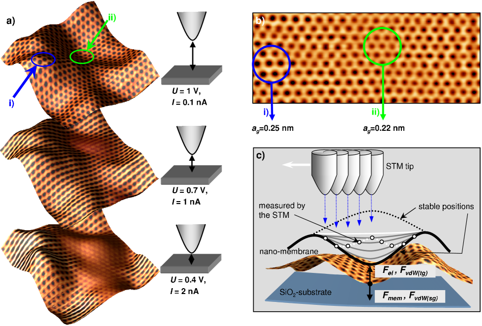
The morphology of graphene has been studied previously by STM Geringer ; Ishigami ; Stolyarova ; Zhang . By comparing with the morphology of SiO2, we revealed that graphene can exhibit an intrinsic rippling not induced by the substrate. We argued that the rippling appears, if graphene is freely suspended between hills of the SiO2 Geringer . The rippling (amplitude: 0.3-0.5 nm) exhibits a preferential wave length of 15 nm at 300 K, Geringer slightly increased at 4.8 K to 20 nm. At smaller length scales, we observe additional corrugation of 70 pm. Figure 1a shows this corrugation at several tip-sample distances. At large distance (top), the corrugated surface and the typical carbon hexagons are visible. Interestingly, the apparent lattice constant differs by 14 % between oppositely curved areas (Fig. 1b). This is explained by the tilting of the pz-orbitals within the curved surface assuming an effective pz-length of nm in accordance with theory Balatsky .
Decreasing the tip-graphene distance (middle, Fig. 1a), a small bump appears within the valley, which at even smaller distance (bottom) increases in height and diameter. With respect to the neighbouring hill, the valley is lifted by 32 pm, i.e. about half of the initial height difference hill-valley. Within the lifted area, the atomic structure changes from hexagons to bumps appearing at every second atom position, which has been checked by following up lines of atomic corrugation. The symmetry between A and B lattice is broken, most probably due to in-plane compressive stress. An explanation is sketched in Fig. 1c: the electrostatic and vdW force of the tip (, ) lift the graphene valley until compensated by the restoring elastic force of the membrane and the vdW force of the substrate. Since the two tip forces change with lateral tip position, a dynamic image of the lifting results as indicated by white dots in Fig. 1c. While a hill appears within the STM image, the membrane still maintains its valley-like shape, but with reduced curvature. The resulting compressive, lateral force within the lifted area can be reduced by a vertical zig-zag atomic arrangement straightforwardly explaining the observed symmetry breaking between A and B lattice.
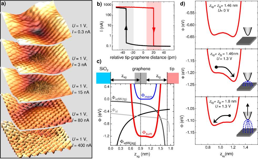
While the membrane’s lifting in Fig. 1 is reversible, other valleys exhibit hysteresis. Figure 2b shows the -curve of a hysteretic area at a sample voltage of V. While approaching or retracting the tip, a jump in current by three orders of magnitude is observed with a hysteresis of pm. Such hysteretic membranes can be identified directly within constant-current images, if is chosen within the bistable range. This is demonstrated in Fig. 2a, where a valley (hill) showing atomic hexagons is visible at low (high) , while a noisy area appears in between. The noisy behaviour is caused by the feedback loop, i.e. the tip approaches which increases the tip forces and induces a snapping of the membrane towards the tip; this increases by three orders of magnitude and the tip retracts again leading to reduced tip forces and a snapping back of the membrane. We observed bistability only in valleys and never on hills. Although analysing several tens of valleys, we could not find any correlation between hysteretic or reversible behaviour and depth, width or curvature of the valleys. Thus, we conclude that graphene-substrate interactions not visible by STM are crucial.
In order to model the observed behaviour, we analyse the involved interaction potentials. Besides the electrostatic potential between tip and graphene, the vdW potentials for tip/graphene and graphene/SiO2 Israel , and the elastic potential of the membrane are considered (see methods). They are plotted in Fig. 2c as a function of vertical graphene position for a fixed tip-substrate distance (1.63 nm). The summed up potential exhibits two local minima representing the observed bistability. Fig. 2d shows two nearly degenerate minima at V and tip-substrate distance nm (top). The lower minimum transforms into a saddle at V (middle) forcing the membrane to the upper minimum, i.e. 0.34 nm closer to the tip. Increasing now the tip-graphene distance by 0.34 nm (reduced ) shakes the potential back and the membrane flips back to its original minimum (bottom). Note that nm is estimated by extrapolation of towards the contact conduction Berndt leaving only the initial substrate-graphene distance nm as a fit parameter. By decreasing the initial to nm, we still calculate two minima, but we are not able to switch the membrane to the upper position by reasonable . This explains the reversible behaviour observed in Fig. 1.
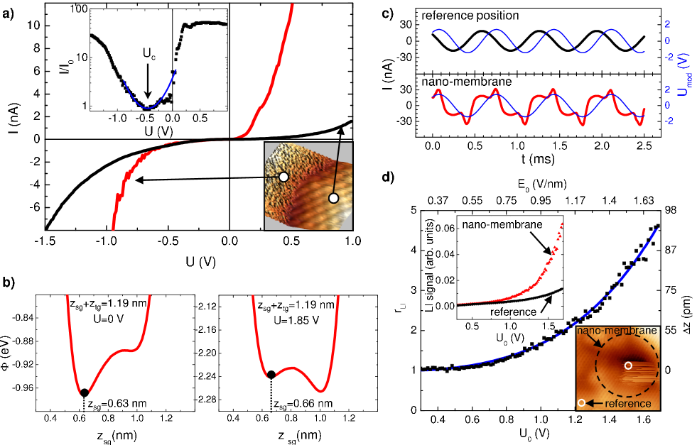
To explore the electric response of the membrane, we varied . First, we measured on a hysteretic valley in comparison with on a hill (Fig. 3a). Assuming the same electronic structure at both positions, the ratio of the two curves is given by , where is the electron’s decay constant determined within the supplement. Thus, the logarithmic plot of directly displays the deflection of the valley with respect to the hill (upper inset, Fig. 3a). The minimum of marks the absence of electrostatic force at the contact potential V implying a tip work function of 5.11 eV (graphene: 4.66 eV Bin ).
Next, we apply an ac-voltage with varying amplitude at a dc-offset V and fixed tip-substrate distance. The tip is placed above the nano-membrane marked by the dashed circle in the inset of Fig. 3d. We choose nA low enough to avoid snapping of the membrane. Figure 3c shows the resulting and the applied for the membrane (bottom) and on a reference (hill) position (top). At reference, is dominated by the capacitive crosstalk (phase shift of ). At the membrane, an additional in-phase signal, non-linear with respect to , indicates the reversible membrane movement. Fig. 3b displays the corresponding at the two extrema of electrostatic force ( nm). The membrane does not switch between the two minima, but oscillates reversibly within one valley in agreement with experiment.
Finally, we use lock-in technique to measure the deflection amplitude with respect to . The inset of Fig. 3d shows the lock-in output measured on the nano-membrane (red) and on a reference position (black). The stronger signal at the membrane again indicates its oscillatory motion. To get rid of unknown parameters we use the ratio of the two lock-in signals
| (1) |
From we deduce numerically (see supplement) as displayed on the right scale of Fig. 3d. The maximum amplitude is higher than expected from the model in Fig. 3b. This is likely caused by the fact that also the hills are simultaneously lifted by the tip forces, which continuously decreases with respect to our model. Nevertheless, the displayed and the corresponding electric field amplitude deduced from and (see supplement) give an impression of the amplitude-field relation achievable by external excitation.
The basic resonance frequency of the nano-membrane can be roughly estimated by clamped membrane theory using N/m Lee , membrane radius nm, and mass kg and assuming HOPG values for thickness nm, and Poisson-ratio Robinson :
| (2) |
More adequate molecular dynamics simulations (MDS) for monolayer graphene reveal GHz for a smaller area (4.3 nm2) exhibiting 75 % deviation from eq. 2 Inui . Anyhow, the nano-membranes consisting of only 200-800 atoms are ideal resonators for ultra sensitive mass detection. Adsorbing one hydrogen atom of mass would lead to a relative frequency-shift of
| (3) |
MDS finds quality factors for unsupported graphene monolayers at 300 (3) K Kim2 . Experiments reveal lower values for multilayer graphene probably due to interlayer friction Bunch ; Sanchez ; Bunch2 ; Peng , but has been achieved using oxidized multilayer graphene at 300 K Robinson . This might be sufficient to detect frequency shifts of . Measuring membrane oscillations would be eased by the nonlinearity of requiring only dc detection, but the excitation in the range of 100 GHz remains a technical challenge.
I methods
The preparation of the graphene sample is done by mechanical exfoliation on a SiO2 substrate as described elsewhere Novo ; Lemme . A graphene flake containing a monolayer region is identified by an optical microscope. In addition, the film thickness is confirmed by Raman spectroscopy Geringer . A gold contact surrounding the graphene is produced by e-beam lithography. In order to remove the residual resist and adsorbates as water, the sample is heated to 170∘C for a few hours, first in air, and then, directly before the measurement, in ultra-high vacuum ( mbar). The monolayer region of m2 is positioned below the tip of the STM by a piezo motor using the control by an optical long distance microscope with a resolution of 5 m. The measurements are performed with a high resolution STM operating at K Mashoff . The tip is prepared prior to measurements by applying voltage pulses and field emission on the gold contact region. All STM images are measured in constant-current mode with the voltage applied to the sample. All spectroscopic curves are measured with the feedback switched off at stabilization voltage and stabilization current . Afterwards, either or the tip sample distance is changed, while measuring the tunnelling current .
Calculations of the interaction potentials acting on the graphene membrane are described in detail in the supplement. In short, we use a dielectric plane for SiO2, a metallic circle of cosine shape in vertical direction for the membrane and a metallic W tip of parabolic shape (central radius: nm) to calculate the vdW potentials Israel . The elastic potential is modelled by a clamped membrane implying with taken from experiment Lee and being the membrane deflection. We assume two minima (two relaxed membrane positions) of two -curves with origins separated by 0.12 nm in order to describe the fact that the membrane is first laterally compressed by lifting with respect to the hills, but is relaxed again after being higher than the surrounding hills. We do not include a pretension term Lee , since pretension is given explicitly by the vdW forces. The electrostatic energy is calculated using as the tip-nano-membrane capacitance modelled as a sphere in front of a plane and as the voltage drop between tip and graphene reduced with respect to due to graphene’s finite carrier density.
II acknowledgement
We appreciate financial support of the German Science foundation via Mo 858/8-1.
III Supplementary information
III.1 Determination of the initial tip/graphene distance and the decay constant
The absolute distance between tip and graphene obtained after stabilization, , could be determined, in principle, by decreasing the distance between tip and sample until the conductance reaches the conductance quantum Berndt . Unfortunately, this does not work for graphene, because the graphene is lifted during the tip approach, even on the hills (reference positions) as indicated from significantly too large decay constants extracted from -spectra, which have been measured systematically on the graphene surface. The only way to reasonably estimate is to calculate nm-1 with the help of equation 5 (below) and, then, to extrapolate the exponential behaviour of the conductance with respect to the distance by using the stabilization parameters V and pA:
| (4) |
To determine the decay constant , we use a planar tunnelling junction with a correction factor Ukraintsev :
| (5) |
The effective work function eV has been calculated using the known graphene work function of eV Bin and a tip work function of eV derived from the measured contact potential as displayed in Fig. 3a of the main text. The correction factor has been determined by fitting -curves measured with the same microtip on Au(111) by equation 5 (work function: eV Mich ).
III.2 Calculation of the interaction potentials acting on the nano-membrane
In order to describe the observed behaviour of the nano-membrane, the involved interaction potentials are analyzed in detail. Besides the electrostatic potential induced by the tip, the Casimir/van-der-Waals potentials induced by the tip and the SiO2-substrate as well as the elastic restoring force of the membrane itself are considered.
III.2.1 Casimir/van-der-Waals potential induced by the tip
The description of the van-der-Waals and Casimir potential per unit area between two materials is given by Bordag :
| (6) | |||||
where and denote the frequency dependent reflection coefficients of graphene and tungsten, respectively, is the wave number parallel to the surface, is the variable distance between graphene and the tip apex and is the frequency (: Planck’s constant). The reflection coefficient of graphene can be calculated by Bordag :
| (7) |
with m-1, m/s and
| (8) |
To determine the reflection coefficient of the tungsten tip, the frequency dependent dielectric constant has to be used:
| (9) |
with
| (10) |
The dielectric function can be approximated knowing the plasma frequency of tungsten Hz Ordal :
| (11) |
The total interaction potential is determined by an integration of equation 6 over the circular area of the nano-membrane:
| (12) |
where denotes the vertical distance between tip and graphene at a lateral distance measured from the centre of the membrane and indicates that we use the tip-graphene distance in the centre of the membrane as the variable for . Assuming a circular membrane with the measured radius of nm and a 2D-cosine shaped corrugation (see figure S1), as well as a parabolic tip with central radius , can be described as:
| (13) |
The vertical distance between tip apex and the hills surrounding the membrane is determined by analyzing the measured valley depth with respect to the surrounding hills. For the tip radius we can only give an upper limit of nm determined by analyzing STM images of atomically resolved valleys, which would not have been resolved by larger tips due to convolution effects. The smallest possible tip radius of nm is given by a tetraedric alignment of the first four atoms. For the calculation, we use a value of nm, determined as described below.
![[Uncaptioned image]](/html/0909.0695/assets/x4.png)
S1: Definition of distances used in the calculation of the interaction potentials.
III.2.2 Casimir/van-der-Waals potential induced by the SiO2-substrate
The interaction potential between graphene and the amorphous SiO2-subtrate is calculated similarly using equation 610 and 12, but replacing by the distance between graphene and the SiO2 substrate as well as by the reflection coefficient of SiO2 . In case of an insulating material like SiO2, is given by another expression Bordag :
| (14) |
where is the main electronic absorption frequency being within the ultra violet region Israel ; Heraeus . For amorphous SiO2, we use the known dielectric constant at zero frequency of Wilk . To describe , assuming a plane substrate and again a 2D-cosine shaped membrane as sketched in Fig. S1, we use
| (15) |
with being the distance between substrate and the borders of the membrane (surrounding hills) and being the distance between the substrate and the lowest point of the membrane. The value of can vary with the applied voltage or with the tip-substrate distance. However, the change of with or tip-substrate distance can be measured via the tunnelling current. Only the offset of the initial tip-substrate distance, , without electric field has to be taken as a fit parameter.
III.2.3 Elastic membrane potential
In order to determine the elastic potential of the nano-membrane, we assume a cubic force dependence of the deflection as given by the classical clamped membrane theory according to Komaragiri et al. Komaragiri Lee . The nanomembrane gets laterally compressed if lifted until the centre of the membrane is at the same height as the surrounding hills (see Fig. 1c of the main text). If lifted further the membrane gets relaxed again up to a second stable position above the surrounding hills. In order to model this behaviour, we compose the membrane potential of two parts and with minima vertically symmetric with respect to the position of largest compression leading to:
where denotes the two dimensional Young’s modulus due to compressing or stretching of the atomic bonds, which has been measured previously to be N/m Lee . The distance between the two potential minima is the second free parameter of our model, only limited to about twice the valley depth. We found that nm is able to reproduce the behaviour of the membranes displayed in Fig. 1 and 2 of the main text. This number is lower than the valley depth appearing in the STM images implying that the van-der-Waals force of the SiO2 substrate increases the corrugation strength within the graphene flake.
III.2.4 Electrostatic potential induced by the tip
The electrostatic potential induced by the tip is given by
| (16) |
with the capacitance and the effective gap voltage to be determined. We approximate the tip-sample system by a capacitor consisting of a sphere with radius above a circular plate of radius corresponding to tip and membrane, respectively. The capacitance for can be calculated analytically resulting in Smythe :
| (17) | |||||
with the distance between the tip apex and the infinite plate . The capacitance determined by equation 17 has to be modified because of the finite area of the nano-membrane below the tip. Therefore, we assume a Gaussian shape of the total charge density of the infinite plate with a maximum at to be determined below and calculate the capacitance of the finite membrane by integration only over the circular area of the nano-membrane. We end up with a capacitance of
| (18) |
Because of the finite charge carrier concentration of graphene, the effective voltage between the tip and graphene is smaller than the applied bias-voltage . The remaining voltage leads to a considerable Fermi level shift within the graphene until the charge carrier density is high enough to screen the electric field. As a consequence, there is a potential drop between the graphene just below the STM tip and the gold electrode connected to the external power supply. Due to the linear dispersion relation of graphene the two dimensional charge carrier density can be written as Gusy :
| (19) |
where with being the contact potential determined in Fig. 3a of the main text, m/s is the Fermi-velocity of graphene and is the electron’s charge. In equilibrium, the electrons screen the electric field and the resulting 2D charge density can be most easily approximated by a plate capacitor leading to:
| (20) |
Thereby, denotes the distance between the plate and the centre of mass of the lower half sphere approximating the tip, which has been chosen to map the model of two parallel plates to the model of a sphere and a plate. With the help of equations 19 and 20, the effective voltage drop between tip and graphene becomes:
| (21) | |||||
The value of the dielectric constant for graphene on SiO2 has been calculated previously using the image potential method and amounts to Xu . The resulting calculated straightforwardly by inserting into equation 19 has been used self-consistently as the maximum of the Gaussian charge density required to calculate .
III.3 Excitation of the nano-membrane by ac-voltage
We applied an ac-voltage with a varying amplitude , at a dc-offset and a frequency of kHz. In addition, we define the voltage including the contact potential determined from Fig. 3a of the main text. The time dependent tunnelling currents , measured at the stable reference position and measured above the nano-membrane can be described using the linear graphene density of states as:
| (22) |
and
| (23) |
where denotes the deflection of the nano-membrane with respect to its position in the absence of electric field and is the part of the corrected voltage dropping between membrane and tip. Note, that the expression for is assumed not to be present on the reference position. The quadratic dependence of the tunnelling current with respect to the bias voltage is derived from the linear dispersion relation of graphene and has been checked by according fits to the measured -spectra. In Fig. 3d of the main text, we display the lock-in ratio:
| (24) |
which can be directly used to determine the deflection amplitude numerically as displayed on the right of Fig. 3d of the main text. Accordingly, the upper scale of Fig. 3d of the main text shows the electric field amplitude given by with being the minimal distance between graphene and tip and being the maximal effective voltage during the oscillation.
Finally, we describe our estimate of the tip radius . Therefore, we use the simplified clamped membrane model for the force-deflection curve, consisting of a linear term caused by so-called pretension and a cubic term describing the compression of the atomic bonds given by Lee . The equilibrium between the electrostatic force and the elastic membrane force is then given by:
| (25) |
where denotes the two dimensional pretension. After solving towards numerically, we fitted the measured taking and the tip radius as the only free parameters. The excellent fit displayed in Fig. 3d of the main text results in a tip radius of nm and a pretension of N/m.
References
- (1) Bunch, J. S. et al. Electromechanical Resonators from Graphene Sheets. Science 315, 490 (2007).
- (2) Lavrik, N. V. & Datskos, P. G. Femtogram mass detection using photothermally actuated nanomechanical resonators. Appl. Phys. Lett. 82, 2697 (2003).
- (3) Ilic, B. et al. Attogram detection using nanoelectromechanical oscillators. J. Appl. Phys. 95, 3694 (2004).
- (4) Peng, H. B., Chang, C. W., Aloni, S., Yuzvinsky, T. D. & Zettl, A. Ultrahigh Frequency Nanotube Resonators. Phys. Rev. Lett. 97, 087203 (2006).
- (5) Jensen, K., Kim, K. & Zettl, A. An atomic-resolution nanomechanical mass sensor. Nature Nanotechn. 3, 533 (2008).
- (6) Bunch, J. S. et al. Impermeable Atomic Membranes from Graphene Sheets. Nano Lett. 8, 2458 (2008).
- (7) Novoselov, K. S. et al. Electric Field Effect in Atomically Thin Carbon Films. Science 306, 666 (2004).
- (8) Geringer, V. et al. Intrinsic and extrinsic corrugation of monolayer graphene deposited on SiO2. Phys. Rev. Lett. 102, 076102 (2009).
- (9) Meyer, J. C. et al. The structure of suspended graphene sheets. Nature 446, 60 (2007).
- (10) Lee, C., Wei, X., Kysar, J. W. & Hone, J. Measurement of the Elastic Properties and Intrinsic Strength of Monolayer Graphene. Science 321, 385 (2008).
- (11) Komaragiri, U., Begley, M. R. & Simmonds, J. G. The Mechanical Response of Freestanding Circular Elastic Films Under Point and Pressure Loads. J. Appl. Mech. 72, 203 (2005).
- (12) Wan, K.-T., Guo, S. & Dillard, D. A. A theoretical and numerical study of a thin clamped circular film under an external load in the presence of a tensile residual stress. Thin Solid Films 425, 150 (2003).
- (13) Kleckner, D. et al. Creating and verifying a quantum superposition in a micro-optomechanical system. New. J. Phys. 10, 095020 (2008).
- (14) Anghel, D. V. & Kühn, T. Quantization of the elastic modes in an isotropic plate. J. Phys. A: Math. Theor. 40, 10429 (2007).
- (15) Stolyarova, E. et al. High-resolution scanning tunneling microscopy imaging of mesoscopic graphene sheets on an insulating surface. Proc. Natl. Acad. Sci. 104, 9209 (2007).
- (16) Ishigami, M., Chen, J. H., Cullen, W. G., Fuhrer, M. S. & Williams, E. D. Atomic Structure of Graphene on SiO2. Nano Lett. 7, 1643 (2007).
- (17) Zhang, Y. et al. Giant phonon-induced conductance in scanning tunnelling spectroscopy of gate-tunable graphene. Nature Mat. 4, 627 (2008).
- (18) Wehling, T. O., Grigorenko, I., Lichtenstein, A. I. & Balatsky, A. V. Phonon-Mediated Tunneling into Graphene. Phys. Rev. Lett. 101, 216803 (2008).
- (19) Israelachvili, J. Intermolecular and Surface Forces, 2nd edition (Academic Press Limited, London, 1992).
- (20) Shan, B. & Cho, K. First Principles Study of Work Functions of Single Wall Carbon Nanotubes. Phys. Rev. Lett. 94, 236602 (2005).
- (21) Kröger, J., Jensen, H. & Berndt, R. Conductance of tip surface and tip atom junctions on Au(111) explored by a scanning tunnelling microscope. New J. Phys. 9, 153 (2007).
- (22) Robinson, J. T. et al. Wafer-scale Reduced Graphene Oxide Films for Nanomechanical Devices. Nano Lett. 8, 3441 (2008).
- (23) Inui, N., Mochiji, K. & Moritani, K. Actuation of a suspended nano-graphene sheet by impact with an argon cluster. Nanotechnology 19, 505501 (2008).
- (24) Kim, S. Y. & Park, H. S. The Importance of Edge Effects on the Intrinsic Loss Mechanisms of Graphene Nanoresonators. Nano Lett. 9, 969 (2009).
- (25) Garcia-Sanchez, D. et al. Imaging Mechanical Vibrations in Suspended Graphene Sheets. Nano Lett. 8, 1399 (2008).
- (26) Lemme, M. C., Echtermeyer, T. J., Baus, M. & Kurz, H. A Graphene Field-Effect Device. IEEE Electron Device Lett. 28, 282 (2007).
- (27) Mashoff, T., Pratzer, M. & Morgenstern, M. A low-temperature high resolution scanning tunneling microscope with a three-dimensional magnetic vector field operating in ultrahigh vacuum. Rev. Sci. Instrum. 80, 053702 (2009).
- (28) Ukraintsev, V. A. Data evaluation technique for electron–tunneling spectroscopy. Phys. Rev. B 53, 11176 (1996).
- (29) Michaelson, H. B. The work function of the elements and its periodicity. J. Appl. Phys. 48, 4729 (1977).
- (30) Bordag, M., Geyer, B., Klimchitskaya, G. L. & Mostepanenko, V. M. Lifshitz–type formulas for graphene and single–wall carbon nanotubes: van der Waals and Casimir interactions. Phys. Rev. B 74, 205431 (2006).
- (31) Wilk, G. D., Wallace, R. M. & Anthony, J. M. High– gate dielectrics: Current status and materials properties considerations. Appl. Phys. Rev. 89, 5243 (2001).
- (32) Ordal, M. A., Bell, R. J., Alexander, Jr., R. W., Long, L. L. & Query, M. R. Optical properties of fourteen metals in the infrared and far infrared: Al, Co, Cu, Au, Fe, Pb, Mo, Ni, Pd, Pt, Ag, Ti, V, and W. Appl. Opt. 24, 4493 (1985).
-
(33)
Webpage of Heraeus, http://www.heraeus-quarzglas.de/en/quarzglas/opticalproperties/
Optical_properties.aspx - (34) Gusynin, V. P. & Sharapov, S. G. Transport of Dirac quasiparticles in graphene: Hall and optical conductivities. Phys. Rev. B 73, 245411 (2006).
- (35) Xu, W., Peeters, F. M. & Lu, T. C. Dependence of resistivity on electron density and temperature in graphene. Phys. Rev. B 79, 073403 (2009).
- (36) Smythe, W. R. Static and Dynamic Electricity, 3rd Edition. (Mc Graw-Hill Inc., 1968).