Improving the Coherence Time of Superconducting Coplanar Resonators
Abstract
The quality factor and energy decay time of superconducting resonators have been measured as a function of material, geometry, and magnetic field. Once the dissipation of trapped magnetic vortices is minimized, we identify surface two-level states (TLS) as an important decay mechanism. A wide gap between the center conductor and the ground plane, as well as use of the superconductor Re instead of Al, are shown to decrease loss. We also demonstrate that classical measurements of resonator quality factor at low excitation power are consistent with single-photon decay time measured using qubit-resonator swap experiments.
Superconducting coplanar resonators have many important applications such as photon detection day2003 and quantum computation wall2004 ; sill2007 , and recently have been used to host arbitrary photon states generated by coupling to qubits hofh2008 ; wang2008 ; hofh2009 . A key parameter limiting the performance is the energy relaxation time , while dephasing is relatively unimportant wang2009 . Resonator performance has typically been determined through classical measurements of the quality factor, and much work has yet to be done to understand the physics of the loss mechanisms and to optimize resonator designs for best performance gao20081 ; gao20082 ; bare2008 ; heal2008 ; chen2008 .
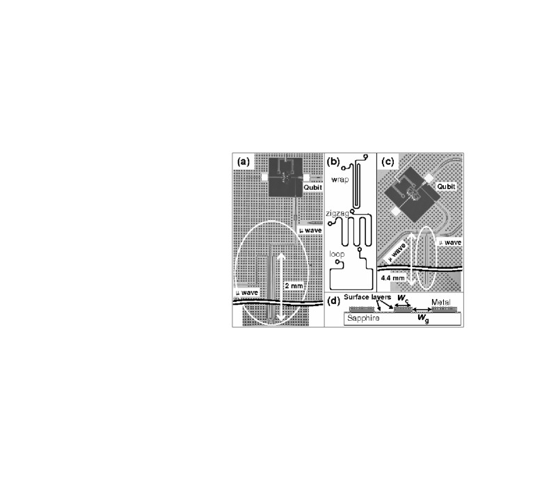
Here we show how several previously untested loss mechanisms can be eliminated or optimized to reach a measured quality factor in the 200,000 to 400,000 range at low power, while the intrinsic quality factor is even higher after subtraction of the coupling capacitor limited . We provide detailed evidence that surface loss from two-level state (TLS) defects is an important loss mechanism. Finally, we show how relatively simple quality factor measurements, when taken at low power, can be used to predict the energy decay time of resonators at the single photon level.
For this work, we measured various half-wavelength () and quarter-wavelength () coplanar resonators, as described in Fig. 1 and Table 1. Aluminum (Al) films were sputter deposited and etched with a -based reactive ion etch (RIE), whereas Rhenium (Re) was electron-beam evaporated in a molecular beam epitaxy system using a substrate temperature of 850 ∘C and etched with -based RIE. The films were fabricated as part of a multilayer process to enable testing with qubits. of the resonators was determined in an adiabatic demagnetization refrigerator using standard two-port transmission measurements with a vector network analyzer. ’s estimated from the calibration were 400,000 (1,000,000) for () resonators but were not subtracted from .
| metal, geometry | ||||||
| (m) | (m) | (GHz) | (k) | (s) | (s) | |
| Re, , loop | 5 | 2 | 6.3 | 100 | 2.5 | 2.0 |
| Re, , zigzag | 5 | 2 | 6.6 | 40 | 1.0 | 1.0 |
| Re, , wrap | 5 | 2 | 6.6 | 90 | 2.3 | 3.5 |
| Re, , zigzag | 10 | 4 | 6.8 | 200 | 5.1 | 5.1 |
| Al, , loop | 5 | 2 | 6.7 | 60 | ||
| Al, , wrap | 5 | 2 | 7.0 | 60 | ||
| Al, , zigzag | 10 | 4 | 7.1 | 110 | ||
| Re, , straight | 5 | 2 | 6.8 | 150 | ||
| Re, , straight | 8 | 3.2 | 6.9 | 210 | ||
| Re, , straight | 16 | 6.4 | 7.0 | 330 | ||
| Re, , straight | 16 | 12 | 7.0 | 230 | 5.8 | 6.4 |
| Al, , straight | 5 | 2 | 7.0 | 72 | ||
| Al, , straight | 8 | 3.2 | 7.0 | 110 | ||
| Al, , straight | 16 | 6.4 | 7.1 | 170 |
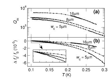
For all the resonators we observed an increase in as the measurement power increased and temperature decreased. The dependence is shown in Fig. 2(a) for representative resonators, taken with high excitation power. To avoid complications due to different geometries, we base most of the discussion on resonators as they share a similar shape. The decrease in with increasing temperature is consistent with quasiparticle dissipation. In Fig. 2(b), the fractional change in the resonance frequency tends to level off around 100 mK, and its magnitude scales inversely with the center trace width, , which is consistent with the kinetic inductance theory gao2006 . The monotonic variation of resonance frequency (Fig. 2(b), inset) is slightly different than previous studies on Nb resonators gao20081 ; bare2008 ; heal2008 , which showed a slight downturn at temperatures below due to TLS.
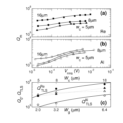
In Fig. 3(a) and (b) we plot versus excitation voltage. Note that increases slightly by about a factor of 2 to 3 for an increase in power by a factor . An increase is naturally explained by TLS loss, which scales with the electric field as , where is a saturation field for TLS loss. For a coplanar resonator with a non-uniform field distribution ocon2008 , numerical calculations indicate that TLS loss at the surface of the metal can be well approximated by , where is the root-mean-squared voltage on the center conductor, , and supplement .
To explain the weak power dependence, we postulate an additional loss mechanism that is independent of power. We find the data can be well fit with parameters and that are plotted in Fig. 3(c) for both the Re and Al films, along with their dependence on the coplanar gap width . We note that estimated from fitted (not shown) is consistent with previous measurements mart2005 ; gao2007 ; ocon2008 ; supplement . We find for both the Re and Al resonators increases with larger , and the TLS loss from Re is approximately three times lower than for Al, suggesting that TLS loss comes from the metal surface of the resonator. scales with since the ratio of the total resonator energy stored in the surface layer gao20081 , as shown by the fits (solid lines) in Fig. 3(c). Additionally, the magnitude of is explained by a 3 nm-thick oxide on the Al metal with a loss tangent , reasonably close to previous findingsmart2005 ; ocon2008 . We expect Re, which is much less reactive than Al, to have a thinner oxide, although both films may be covered by a few-monolayer thick film of water and/or stray contaminants. We also find that Re and Al have similar background loss , which arises from coupling, radiation, non-equilibrium quasiparticles, magnetic vortices, and possibly other unknown mechanisms. may also be partly due to surface loss in the substrate supplement . Since and have similar magnitudes, TLS loss is not dominant even at the lowest power, possibly explaining the absence of a downturn in versus , shown in Fig. 2(b).
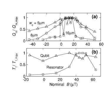
Although a wider gap suppresses TLS loss, care must be taken not to introduce loss from trapped vortices, created when the film is cooled through its superconducting transition stan2004 ; song2009 . The effect of the applied field on is shown in Fig. 4(a), which is consistent with the requirement that the cooling field must be reduced as the center trace widens. This condition indicates a preference for narrow trace widths and holes in the ground plane. We note that using -metal shielding does not guarantee low magnetic fields at the sample because components, such as microwave connectors with plated Ni, may introduce stray magnetic fields. We found that all data had to be taken after optimizing the applied field for maximum .
The effect of different resonator geometries are listed in Table 1. We do not find a significant systematic dependence, suggesting that radiation effects are small with these devices.
Does actually predict the energy decay rate of a single photon? In Table 1 we compare the resonator decay time , determined at low power, with the measured single-photon decay time from the qubit-resonator swap experiment wang2008 . Good agreement is found for the subset of our data where resonators and qubit-resonator devices were fabricated on the same wafer. The single-photon measurements provide the most stringent measure since elevated temperatures or powers typically increase the apparent in resonators.
In conclusion, we have identified several loss mechanisms in superconducting coplanar resonators. The layout geometry has been determined to be unimportant at present loss levels, but loss from trapped superconducting vortices must be minimized by using narrow traces and cooling through the transition temperature in an optimized magnetic field. Surface loss from two-level states has been found to be an important decay mechanism, and can be reduced by designing coplanar resonators with wide gaps and by using superconductors with little surface oxide, such as Re.
Acknowledgements. Devices were made at the UCSB Nanofabrication Facility, a part of the NSF-funded National Nanotechnology Infrastructure Network. This work was supported by IARPA under grant W911NF-04-1-0204 and by the NSF under grant CCF-0507227.
References
- (1) P. K. Day, H. G. LeDuc, B. A. Mazin, A. Vayonakis, and J. Zmuidzinas, Nature 425, 817 (2003).
- (2) A. Wallraff et al., Nature 431, 162 (2004).
- (3) M. A. Sillanpää, J. I. Park, and R. W. Simmonds, Nature 449, 438 (2007).
- (4) M. Hofheinz et al., Nature 454, 310 (2008).
- (5) H. Wang et al., Phys. Rev. Lett. 101, 240401 (2008).
- (6) M. Hofheinz et al., Nature 459, 546 (2009).
- (7) H. Wang et al., to be published.
- (8) J. Gao et al., Appl. Phys. Lett. 92, 152505 (2008).
- (9) J. Gao et al., Appl. Phys. Lett. 92, 212504 (2008).
- (10) R. Barends et al., Appl. Phys. Lett. 92, 223504 (2008).
- (11) J. E. Healey, T. Lindstrom, M. S. Colclough, C.M. Muirhead, and A. Y. Tzalenchuk, Appl. Phys. Lett. 93, 3 (2008).
- (12) W. Chen, D. A. Bennett, V. Patel, and J. E. Lukens, Supercond. Sci. Technol. 21, 075013 (2008).
- (13) J. Gao, J. Zmuidzinas, B. A. Mazin, P. K. Day, and H. G. Leduc, Nucl. Instrum. Methods Phys. Res. A 559, 585 (2006).
- (14) A. D. O’Connell et al., Appl. Phys. Lett. 92, 112903 (2008).
- (15) J. M. Martinis et al., Phys. Rev. Lett. 95, 210503 (2005).
- (16) J. Gao et al., Appl. Phys. Lett. 90, 102507 (2007).
- (17) G. Stan, S. B. Field, and J. M. Martinis, Phys. Rev. Lett. 92, 097003 (2004).
- (18) C. Song et al., Phys. Rev. B 79, 174512 (2009).
- (19) For a more detailed discussion of the numerical calculations, see supplementary material at arXiv:0909.0547.
I Supplementary Material
We provide detailed calculations for Ref. S (1), mainly showing how a non-uniform electric field distribution can be accounted for in TLS dielectric loss.
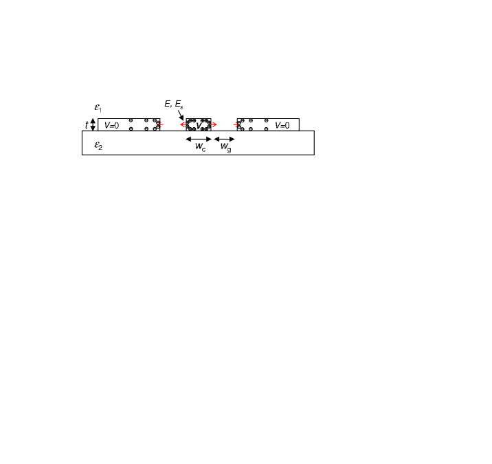
We consider a coplanar resonator with a non-uniform surface charge distribution, with a cross-section as illustrated in Fig. S1. For the case of a uniform dielectric, e.g. , we use matrix inversion of the inverse capacitance matrix, defined through the equation
| (S1) |
to find the surface charge distribution (and thus the field distribution) at position . Here, is the potential at position , set to at the center trace and on ground pads. The separation between elements and is , and is the vacuum permittivity. For , the and regions can be, respectively, conformally mapped into two rectangles where field distributions are easily calculable S (2). We find that both approaches yield similar electric field distributions. Note that fields have tangential components that are continuous at the interface between the two dielectrics. For simplicity, we discuss the results based on uniform dielectrics. Note that these calculations were also checked with commercial software (COMSOL), which were roughly in agreement with our simplified model.
| (m) | (m) | |||
|---|---|---|---|---|
| 5 | 2 | 1.31 | 1.64 | 2.40 |
| 8 | 3.2 | 1.40 | 1.59 | 2.93 |
| 16 | 6.4 | 1.48 | 1.56 | 3.85 |
Most of the energy of the field is concentrated around the gap of the coplanar line. For the = 5 m resonator, for example, of the metal-oxide surface energy is stored within 1 m around the gap region. Finite element analysis using COMSOL shows that of the total resonator energy is stored in the substrate surface and is in the metal surface, assuming a thickness of 3 nm and a dielectric constant of 10 for surface layers.
We now calculate the power dependence of the resonator quality factor coming from dielectric loss of two-level states (TLS) at the metal surface. We first consider the approximation of a uniform electric field coming from the surface region around the middle of the center-trace side wall, as indicated in Fig. S1. From the loss theory of TLS, we find
| (S2) | |||||
where is the saturation field for the TLS, and is a factor obtained from numerical simulations (Eq. S1) and tabulated for three common parameter sets in Table S1. An exact relation is obtained by incorporating the computed field distribution and using a weighted sum of the TLS loss over all exposed metal surfaces
| (S3) |
where the surface fields are proportional to the resonator voltage .
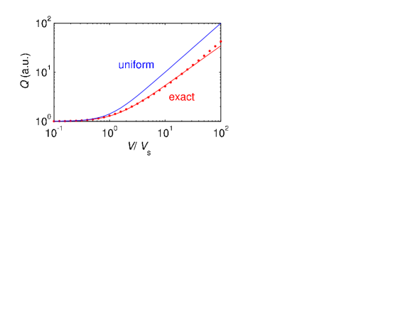
In Fig. S2 we plot (dots) versus for a resonator with = 5 , using the exact field distribution from Eqs. S1 and S3. For reference, from Eq. S2 is also plotted as the blue line. To more simply describe the results of the numerical calculations, we fit a line to the dots at the low voltage region according to
| (S4) |
where and are rescaling factors, obtained from the fits, that are also listed in Table S1. Accordingly, we use to fit the experimental data of versus (or as in Ref. S (1)) such that
| (S5) |
with , , and as fitting parameters. These fit parameters are listed in Table S2. We find that varying slightly does not affect the systematic trend of and , as shown in Fig. 3(c) in Ref. S (1).
From the fitted we obtain the saturation field for the metal surface layer as
| (S6) |
In Table S2 we list the fitted saturation fields ’s from different resonators. They are reasonably close to each other, and have a magnitude close to that of a 250 nm-thick LC pancake resonator from Fig. 1 in Ref. S (3) (taking ), especially considering possible systematic errors in the absolute calibration of the transmission (also see Refs. S (4, 5)).
is power independent and comes from coupling capacitor related loss, vortex loss, and other loss mechanisms. It should also be noted that may also be partly from the surface layer of the sapphire substrate, for which the saturation field might be significantly higher than ’s listed in Table S2. Support of this hypothesis is that also increases with increasing . We tried fitting the data with two ’s of different magnitudes to account for this effect, but it was unsuccessful as it introduced too many degrees of freedom for the limited number of data points. Singling out the substrate surface TLS contribution to will require further measurements.
| (m) | (m) | () | () | (V) | (V/m) | |
|---|---|---|---|---|---|---|
| 5 | 2 | 3.16 | 1.23 | 5.0 | 46 | |
| Al | 8 | 3.2 | 3.85 | 1.41 | 5.4 | 35 |
| 16 | 6.4 | 4.39 | 2.92 | 11.8 | 48 | |
| 5 | 2 | 2.79 | 2.82 | 6.0 | 55 | |
| Re | 8 | 3.2 | 3.33 | 5.43 | 7.8 | 51 |
| 16 | 6.4 | 5.84 | 8.41 | 10.7 | 43 |
Finally we comment on the connection between results from the power measurement (Fig. 3 in Ref. S (1)) and the temperature measurement (Fig. 2 in Ref. S (1)). It has been shown in previous studies (see references in Ref. S (1)) that a downturn in resonance frequency at temperatures below indicates the existence of surface TLS. This feature is missing in our data presumably because we use lower materials (1 K versus 10 K). At the lowest temperatures, the TLS loss mechanism is not dominant (though important) as and are comparable (see Table S2). Measurements of temperature dependence are mostly consistent with quasiparticle dissipation.
References
- S (1) H. Wang et al. “Improving the Coherence Time of Superconducting Coplanar Resonators”, arXiv:0909.0547.
- S (2) J. Gao, Ph.D. thesis, California Institute of Technology (2008).
- S (3) A. D. O’Connell et al., Appl. Phys. Lett. 92, 112903 (2008).
- S (4) J. M. Martinis et al., Phys. Rev. Lett. 95, 210503 (2005).
- S (5) J. Gao et al., Appl. Phys. Lett. 90, 102507 (2007).