Radiation Tolerance of CMOS Monolithic Active Pixel Sensors with Self-Biased Pixels 111Presented at 11th European Symposium on Semiconductor Detectors, June 7 - 11, 2009 at Wildbad Kreuth
M. Deveaux1,
S. Amar-Youcef1,
A. Besson2,
G. Claus2,
C. Colledani2,
M. Dorokhov2,
C. Dritsa1,2,3,
W. Dulinski2,
I. Fröhlich1,
M. Goffe2,
D. Grandjean2,
S. Heini2,
A. Himmi2,
C. Hu2,
K. Jaaskelainen2,
C. Müntz1,
A. Shabetai2,
J. Stroth1,3,
M. Szelezniak4,
I. Valin2 and
M. Winter2
1
Institut für Kernphysik, Johann Wolfgang Goethe-Universität, 60438 Frankfurt, Germany
2
Institut Pluridisciplinaire Hubert Curien (IPHC),
67037 Strasbourg, France
3
Gesellschaft für Schwerionenforschung mbH, 64291 Darmstadt, Germany
4
Lawrence Berkeley National Laboratory, Berceley CA 94720, U.S.A.
Abstract
CMOS Monolithic Active Pixel Sensors (MAPS) are proposed as a technology for various vertex detectors in nuclear and particle physics. We discuss the mechanisms of ionizing radiation damage on MAPS hosting the the dead time free, so-called self bias pixel. Moreover, we discuss radiation hardened sensor designs which allow operating detectors after exposing them to irradiation doses above 1 Mrad.
1 Introduction
The ability of Monolithic Active Pixel Sensors (MAPS) to provide charged particle tracking has been demonstrated with several MIMOSA222Standing for Minimum Ionizing MOS Active pixel sensor. prototypes [1, 2]. The key element of such sensors is the use of an n-well/p-epitaxial diode to collect, through thermal diffusion, the charge generated by the penetrating particles in the thin epitaxial layer located underneath the readout electronics. Tests performed with GeV/c pion beams at CERN proved excellent detection performances. A single point resolution of m and a detection efficiency close to 100%, resulting from a signal-to-noise ratio (S/N) in excess of 30, were routinely observed with various MAPS designs featuring up to 106 pixels on active areas as large as cm2.
MAPS have been proposed as sensor technology for the vertex detectors of the International Linear Collider (ILC), the STAR Heavy Flavor Tracker and the Compressed Baryonic Matter (CBM) experiment. The expected integrated radiation doses of in those application ranges from several ncm2 and few 100 krad (ILC) to up to ncm2 and (CBM). The question whether MAPS for charged particle tracking can stand these doses triggered a joint research program of the IPHC/Strasbourg, the University of Frankfurt and GSI/Darmstadt.
In this work, we will discuss the impact of ionizing radiation on MAPS pixels with a so-called self-biased on-pixel amplifier (SB-pixel) [2]. To do so, we will remind the design and readout principle of this pixel and show up the observed radiation damage effect. Hereafter, we will motivate that all effects observed can be explained as non-trivial consequences of the known radiation induced increase of leakage currents. Finally, we will discuss a radiation hardened pixel structure and show selected test results proving the higher radiation tolerance of this pixel with respect to the standard pixel design.
2 The MAPS operation principle
The sensor of MAPS is formed by a sandwich of three differently P-doped silicon layers, which are the highly doped substrate, the moderately doped epitaxial layer and a highly doped P-well layer found in standard CMOS processes. Due to build-in-voltages, free electrons created by penetrating charged particles are deflected back toward the epitaxial layer when reaching the interface to the highly doped outer layers. The diffusing charge carriers are collected from the thick, non-depleted sensor via a collection diode formed from N-well implantation penetrating the P-well layer.
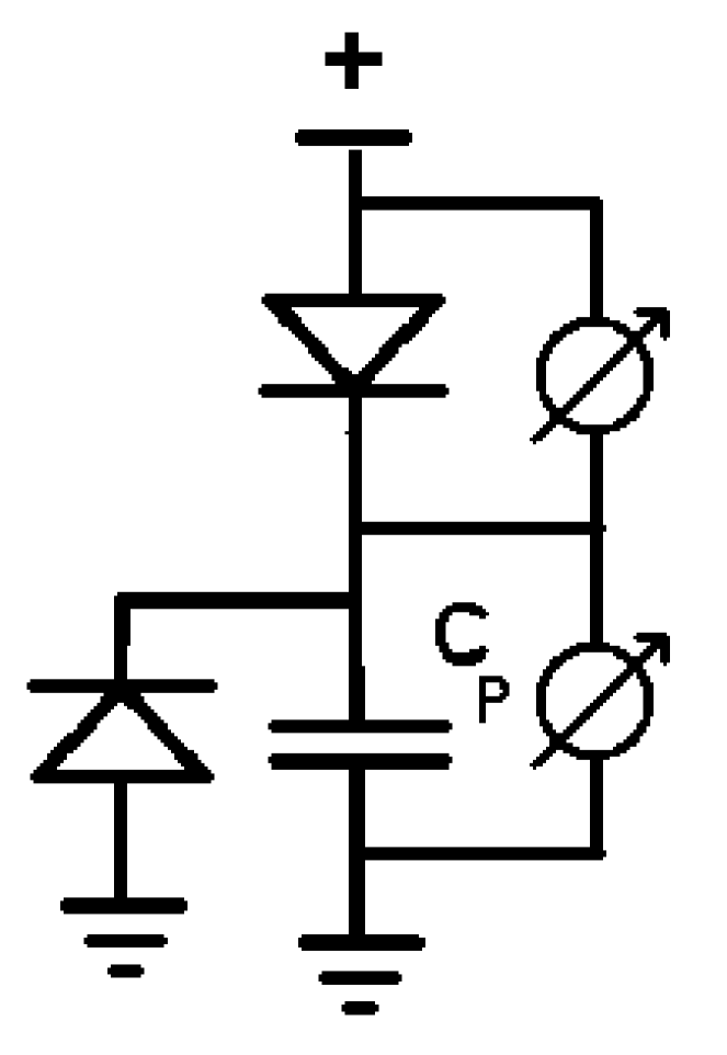
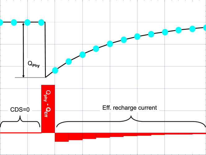
The collected charge is loaded into the parasitic capacity of the pixel amplifier displayed in figure 1(left). The corresponding voltage drop in this capacity is measured by means of a source follower. A high ohmic, forward biased diode is used clear the signal from the pixel and to compensate the leakage current of the collection diode. The clearing process has to be slow with respect to the pixel readout. Therefore, the signal charge remains for several integration cycles in the pixel. The use of Correlated Double Sampling (CDS) avoids a double counting of hits as pixels clearing a signal provide a modest negative signal after CDS. This readout cycle and the response of the SB-pixel to a hit is displayed in figure 1 (right).
3 Ionizing radiation damage in SB-pixels
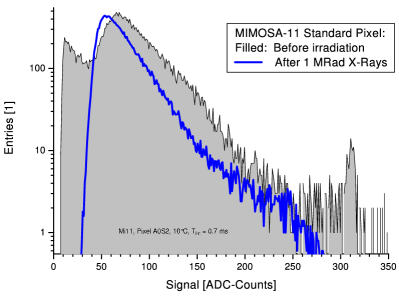
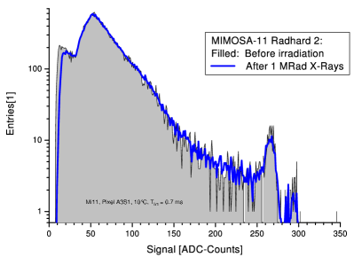
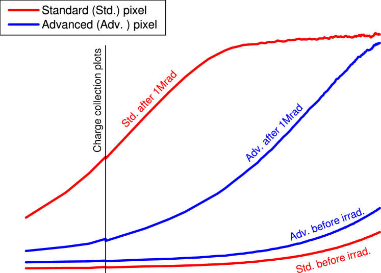
The effects of ionizing radiation on SB-pixels was studied with several generations of MIMOSA prototypes being manufactured in the AMS-0.35 m and AMS-0.35 m OPTO process. The chips were tested with an 55Fe-source, irradiated with the X-ray source of the Institute of Experimental nuclear Physics (IEKP, University of Karlsruhe) and tested again. For radiation doses of up to 1 Mrad, we observed two major effects, which could each alleviated by cooling and reducing the integration time of the sensor: a loss of gain of the pixel, which smeared out the peak corresponding to an interaction of the 55Fe-photon in the small depleted volume of the sensor (see figure 2, left); and increase of noise (see figure 3). At high temperatures, radiation doses and integration times, the noise reached a saturation level of ENC, despite (according to all our experiences) the pixel leakage currents increase further. The saturation stands therefore in contrast to the expected behavior of shot noise, which should scale with . We consider the continuous clearing of the pixel as origin for the misfit between expected and observed behavior of the pixel.
4 The relation between gain loss and leakage current
The accelerated clearing of the pixels (see figure 4) was identified as origin of their effective gain loss. In irradiated pixels, a substantial part of the signal is cleared already before it is read out.
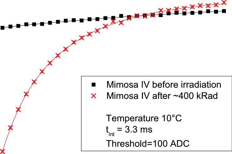
Our measurements show, that this clearing process is well described by an exponential function according to:
| (1) |
In this equation, is the remaining signal charge in the pixel capacity and is the time constant of the pixel. In order to sense the signal before it is cleared, the integration time of the pixel has fulfill (). This is usually assured by the high ohmic design of the biasing diode.
However, as we will motivate in the following, shrinks with increasing leakage current of the pixel (, see figure 1, left). To show this, we assume that the potential drop at the biasing diode is split into a contribution and where is required to drive the equivalent of the leakage current through this diode. The diode fulfills therefore:
| (2) | |||||
| (3) |
In those equations, and is the effective recharge current of the pixel capacity. From the above equations we derive:
| (4) |
Accounting for equation (2), this is equivalent to:
| (5) |
Using the leading order approximation:
| (6) |
and knowing that and , this can be translated to:
| (7) |
The solution of this differential equation fits equation (1) and thus our empiric observation. One identifies:
| (8) |
From this equation one can learn that the radiation induced increase of in MAPS [3] may crucially reduce , which explains the observed acceleration of the pixel clearing.
Note that, due to the rather rough approximation made in equation (6), equation (8) is not straight forwardly suited to predict the absolute value or temperature dependence of . This dependence was addressed by measuring333This was done by illuminating the chip with an Fe55-source and observing the clearing of the pixel. Details of the measurement protocols and additional results are discussed in [4]. as a function of temperature with SB-pixels irradiated with 400 krad X-rays. As shown in figure 5 (left), becomes by more than one order of magnitude shorter when increasing the temperature from -10 ∘C to 40 ∘C, which may be explained by the known strong increase of with increasing temperature. Cooling is therefore an effective mean to alleviate ionizing radiation damage in SB-pixels.
5 Pixels with improved radiation hardness
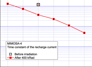
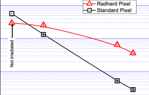
As cooling the sensors is not always feasible, we tried to alleviate the radiation induced increase of by means of modifying the collection diode of the sensor. Our study addressed two presumed sources of radiation induced leakage currents: the thermal generation of e/h-pairs via radiation induced surface defects at Si/SiO2 interfaces close the collection diode; and the appearance of conduction paths along this interface due to a radiation induced positive charge build-up in the SiO2. To suppress those sources, we surrounded the diode with thin gate SiO2, which is known to show only few radiation induced defects with respect to the thicker standard oxide [5]. Silicon guard rings were put to cut the suspected conduction paths, which were assumed to collect e/h-pairs from regions distant to the diode.
The studies were performed with several generations of chips implemented in the AMS 0.35 m - OPTO process (MIMOSA-9,-11, and -15). The design of the diode showing best tolerance to ionizing radiation was inspired by the design of an enclosed transistor [5], where the inner transistor ring is formed by the N-well implantation of the diode. The outer ring is realized with a P-diff implantation, which serves as guard ring cutting potential conduction paths along the Si/SiO2 interface of the chip. A gate (set to ground potential) was placed between both rings to remove any thick SiO2 structures from the vicinity of the collection diode.
The small ( fA) leakage currents of our SB-pixels are not accessible for direct measurements. The improved diode structure were thus benchmarked according to the noise and of the pixels. We found that previous to irradiation, the radiation hardened pixel shows slightly higher noise (see figure 3) and lower (see figure 5, right) than the standard pixel. Given the excellent performances of both designs, this disadvantage is of marginal relevance and vanishes already after a dose of 10 kRad. Hereafter, the radiation hardened pixel showed lower noise and a crucially slower time constant. As expected, the improvement in alleviates the drop in gain observed in the response of the chip to the 55Fe-source (see figure 2, right). This proves that the modified pixel reaches a higher radiation hardness that the standard one.
6 Summary and Conclusion
Within this work, the effects of ionizing radiation MAPS detectors with SB-pixels were discussed. We observed two major effects, which are an increase of shot noise and a drop in the effective gain of the pixel due to an acceleration of its clearing process. As much as the shot noise, the latter effect is caused by the known radiation induced increase of the leakage current of the pixel, which is therefore the only primary radiation damage observed for X-ray doses up to 1 Mrad. All effects can be alleviated substantially by operating the detector with moderate cooling and with small integration time.
We studied different diode structures aiming for reducing the leakage current of irradiated pixels. Best results were achieved by adding two guard rings, a pseudo-gate and a p-diff implantation, around the collection diode. Complementary to the cooling, this structure reduced the shot noise of the pixel and decelerated the clearing process by up to one order of magnitude, which substantially expands the radiation hardness of the sensors.
Acknowledgments
This work was supported by BMBF (06FY1731), GSI (F&E) and the Hessian LOEWE initiative through the Helmholtz International Center for FAIR (HIC for FAIR).
References
- [1] Yu. Gornushkin et al., “Test Results Of Monolithic Active Pixel Sensors For Charged Particle Tracking”, Nucl. Instrum. Meth. A 478, 311 (2002).
- [2] G. Deptuch et al., “Development of monolithic active pixel sensors for charged particle tracking”, Nucl. Instrum. Meth. A 511, 240 (2003).
- [3] M. Deveaux et al., “Charge collection properties of X-ray irradiated monolithic active pixel sensors”, Nucl. Instrum. Meth. A 552, 118 (2005).
- [4] M. Deveaux, “Development of fast and radiation hard Monolithic Active Pixel Sensors (MAPS) optimized for open charm meson detection with the CBM - vertex detector”, PhD thesis, Goethe University Frankfurt/ Université Louis Pasteur Strasbourg (2008).
- [5] W. Snoeys et al. “Layout techniques to enhance the radiation tolerance of standard CMOS technologies demonstrated on a pixel detector readout chip”, Nucl. Instrum. Meth. A 439 349-360 (2000).