Superconductivity in a single C60 transistor
pacs:
74.70.Wz 74.50.+r 73.63.Kv 73.63.RtSingle molecule transistors (SMTs) are currently attracting enormous attention as possible quantum information processing devices Loss:01 ; Romeike:06 ; Heersche:06 ; Jo:06 ; Grose:08 . An intrinsic limitation to the prospects of these however is associated to the presence of a small number of quantized conductance channels, each channel having a high access resistance of at best =12.9 k. When the contacting leads become superconducting, these correlations can extend throughout the whole system by the proximity effect and all contact resistance disappears. This not only lifts the resistive limitation of normal state contacts, but further paves a new way to probe electron transport through a single molecule. In this work, we demonstrate the realization of superconducting SMTs involving a single C60 fullerene molecule. The last few years have seen gate-controlled Josephson supercurrents induced in the family of low dimensional carbon structures such as flakes of two-dimensional graphene Heersche:07 and portions of one-dimensional carbon nanotubes Jarillo:06 . The present study involving a full zero-dimensionnal fullerene completes the picture.
The rapid experimental progress in SMTs has revolutionized our understanding of single-spin magnetism Heersche:06 ; Jo:06 ; Grose:08 , nano-electromechanics Park:00 ; Pasupathy:05 and Kondo correlations Park:02 ; Liang:02 ; Yu:05 ; Roch:08 . However, no experimental realization of superconductivity in a SMT has been reported so far. Superconductivity is a central paradigm to electronic phase coherence phenomena and its effects on SMTs transport properties have been extensively investigated by theory Choi:04 ; Novotny:05 ; Lee:08 . Josephson weak links relying on bottom-up quantum dot (QD) structures could recently be experimentally realized using semiconducting nanowires Doh:05 as well as carbon nanotubes Jarillo:06 ; Cleuziou:06 ; Jorgensen:06 . Superconductivity in a SMT was yet to be observed as it offers new insights into the couplings involved in single molecule junctions. Superconducting correlations have been observed in ungated junctions involving the metallofullerene Gd@C82 Kasumov:05 but the absence of supercurrents have been attributed to the destructive effect of the local magnetic moment carried by the Gd atom on the superconducting phase coherence. In this Letter, we demonstrate the first experimental realization of superconducting single fullerene molecular transistors, in a broad range of coupling strengths to the contacts, covering both the weakly coupled sequential tunneling regime, as well as the resonant tunneling regime.
SMTs are prepared following the electromigration technique Park:99 , further optimized as presented in refs. Park:02 ; Liang:02 ; Yu:05 ; Roch:08 . By extending these advances to measurements at dilution refrigeration temperatures, precise electronic spectroscopies and measurements with superconducting electrodes can be undertaken. The superconducting contacts to the molecular QD are either made of aluminum, or of gold in which superconductivity is induced by the close vicinity of an aluminum capping layer (see Methods for details). After electromigration performed at 4 K, stable devices exhibiting QD behavior are further cooled and measured at 40 mK, with an effective electron temperature of 80 mK. We show here the data on 4 out of 11 samples that were measured at low temperature and which exhibited Coulomb blockade and/or gate-modulated Kondo-like features.

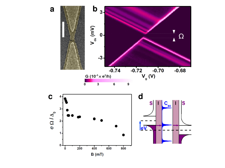
The superconducting weak coupling regime is illustrated in Figure 1b, in a device (sample A) displaying two Coulomb diamonds (CDs). In the absence of other conducting regions near the Fermi level over the experimentally accessible gate voltage window (Vg = -4.5 to +4 V), an addition energy EmeV can be inferred. This brings clear evidence for single molecular quantum dot behavior because a metallic nanoparticle would lead to a much lower addition energy, typically not exceeding some tens of meV Black:96 . At base temperature and zero magnetic field, the conducting regions of device A do not intersect the Fermi level: they are separated by a spectroscopic source-drain voltage gap of about V near the degeneracy point.
This gap, reflecting the quasiparticule spectrum of the contacting electrodes, is a typical feature of a nanostructure weakly coupled to superconducting electrodes Ralph:95 . In such devices, the current is dominated by incoherent sequential tunneling of quasi-particles of energy E (where eV is the bulk superconducting gap of aluminum). The extent of the non-conducting region is very close to 4, as expected in an S-I-S tunneling structure (Figure 1c,d). The source and drain contacts in a SMT usually have a strong geometrical asymmetry in electromigration devices (Figure 1a). In nanostructured aluminum, superconductivity can stabilize up to much higher fields than in bulk material, exceeding 3 T in nanoscaled aluminum particles Black:96 ; one therefore may expect very different critical fields in each contact. This is shown in Figure 1c: rapidly decreases from 4 to about 2 below Hc’ = 40 mT, indicative of one lead going normal, whereas superconductivity in the second lead subsists up to HT, the junction being therefore of N-QD-S type at intermediate fields.

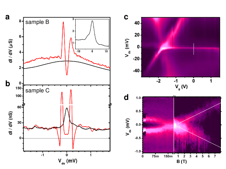
For increasing coupling to the electrodes (i.e. higher conductance, assuming constant asymmetry and number of conducting channels) co-tunneling events can occur at low bias voltage and enhance the conductance via the Kondo effect at low temperature. The increase of the QD DOS by virtue of the Kondo effect originates from quasiparticles in the contacts lying close to the Fermi level, hopping on and off the dot. The Kondo effect and the suppression of the leads’ density of states (DOS) at low energies caused by superconductivity, are therefore rather antagonistic processes. We illustrate the competition between Kondo correlations and superconductivity by two devices, B and C, with Kondo temperatures much larger and lower than Tc respectively. In the normal state of device B, a coulombian addition energy EmeV is observed to coexist with rather strong lead coupling, translating into a large Kondo resonance with TK (Figure 2c, details in the Supplementary Information). In the superconducting state of the leads, superconductivity does not suppress the Kondo resonance and the superconducting features such as the coherence peaks at V superimpose on top of it (Figure 2a). Such a behavior was predicted Glazman:89 ; Choi:04 and previously observed Buitelaar:02 ; Buizert:07 in other types of QD devices verifying . The opposite limit is illustrated by the more weakly coupled device C (Figure 2c), which similarly displayed a Coulomb blockade and Kondo resonance pattern, but with a much lower Kondo temperature TK. In the superconducting state, the Kondo peak at the Fermi level is destroyed Buitelaar:02 ; Choi:04 . Interestingly, inside this CD, corresponding to an odd occupation number, i.e. to a local magnetic moment no longer screened by the lead electrons, the differential conductance is not maximum at . Further, a sign inversion of the differential conductance is observed, which is most prominent close to the degeneracy points. This negative differential conductance, as already reported in larger superconducting QD systems Ralph:95 ; Eichler:07 ; Doh:08 , results from Fermi’s golden rule applied to the superconducting leads’ DOS, which are convoluted with the delta function-like DOS of the QD. The gradual reduction of the superconducting gap under applied magnetic field reestablishes the Kondo resonance, which is further Zeeman split above about 400 mT (Figure 2d).

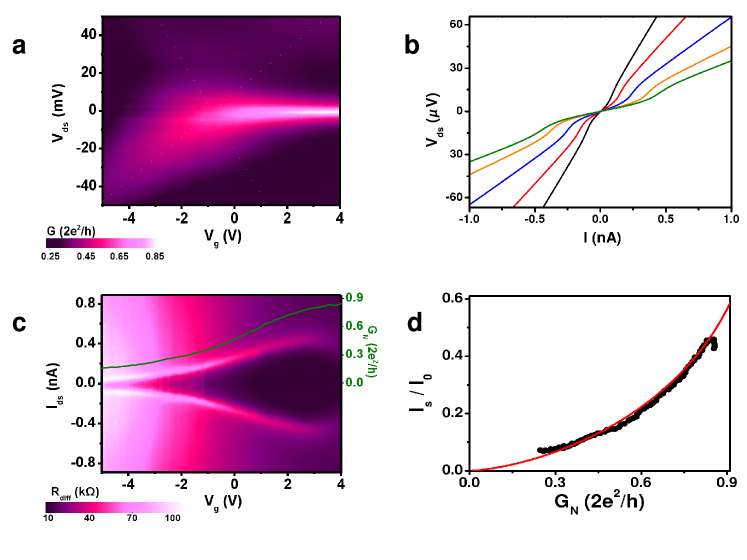
Moving on to high coupling strengths , we show that Josephson supercurrent can be observed in SMTs. In equilibrium, dissipationless transport accross a S-QD-S structure is achieved by co-tunneling of Cooper pairs. The Josephson current amplitude therefore scales with and is experimentally only accessible for relatively strong coupling to the leads. Device D illustrates the molecular junction behavior in this regime. In the normal state (Figure 3a), the differential conductance map exhibits a Kondo resonance for positive gate voltages on a ridge delimited by only faintly visible CD edges. In this regime the electrostatic on-site repulsion is largely overcome by the strong coupling to the leads. The maximum differential conductance observed here approaches the unitary limit, while the width of the Kondo resonance is associated to a large T K, as already reported in normal SMTs in the past Yu:04 ; Yu:05 . In voltage biased measurements of the superconducting state, the differential conductance around the Fermi level displays the usual coherence peaks at with eV (not shown, similar to figure 2a). For supercurrent measurements however, a current bias is better adapted. Figure 3b shows measurements for different gate voltages, showing the gate dependence of the critical current. In further detail, Figure 3c shows a differential resistance map for small bias currents. The ridge visible here defines a switching current such that . For the differential resistance is strongly reduced below . We interpret the residual resistance below as related to phase diffusion of the Josephson state along the ’tilted washboard’ potential [cite]. No hysteresis is observed here which indicates that the Josephson junction is in, or close to, the overdamped limit. The strong reduction of the switching current with respect to the ideal critical current value (equal to 6 to 20 nA here, depending on the gate voltage) is generic to small Josephson junctions, and is understood as an effect of finite temperature and environmental coupling (e.g. to phonons Novotny:05 ). In particular the critical current dependence on the normal state conductance is expected Joyez:94 ; Jarillo:06 to follow
| (1) |
in an unshunted junction hosting a single spin-degenerate conductance channel. Experimentally, this 3/2 power-law dependence was observed to hold in metallic superconducting single electron transistors Joyez:94 and in carbon nanotube junctions Jarillo:06 . The fit of the data shown in figure 3d to (1) yields nA. It is remarkable that whereas the justification of (1) strictly holds for the underdamped regime Joyez:94 , a very good agreement to experiment is still found in our device D.
In conclusion, we have shown a full characterization of C60 SMTs connected to superconducting leads, covering all coupling regimes. The data demonstrate the coexistence and competition of the effects of Coulomb repulsion, Kondo correlations and superconductivity in SMTs for various coupling strengths to the leads. In the most strongly coupled devices, the unitary conductance limit is approached in the normal state and for the first time a gate modulated superconducting current flowing through a single C60 molecule is observed. The observed transport properties are in good agreement with the expected behaviour of a quantum dot connected to superconducting leads. In contrast with previous experiments involving carbon nanotube junctions Jarillo:06 the energy spectrum is fixed by the molecular edifice itself and not by the nanoengineered portion of nanotube linking the contacting electrode. This experiment paves the way for further studies targetting at phase-sensitive measurements and the interplay of superconductivity with magnetically active molecules such as endofullerenes Grose:08 .
METHODS
The starting material for the devices are thin metallic wires with a local constriction about 100 nm wide and 20 nm thick, defined by e-beam lithography and double angle evaporation through a suspended mask, on top of a local Al/Al2O3 backgate (Figure 1a), as described in Roch:08 . C60 diluted in toluene is drop-casted on the thoroughly cleaned devices which are then immediately introduced into the sample mount thermally anchored to the mixing chamber of a dilution refrigerator. At liquid helium temperatures, the bias voltage across the wires is ramped up until the electromigration process sets on. The device resistance, which has an initial value of about 100 , increases, often stepwise, indicating the breaking up of individual 1D atomic conduction channels. As soon as the device resistance exceeds 12.9 k, the bias voltage is cancelled within microseconds. After electromigration, the junctions are further cooled down to sub-0.1 K temperatures. About 50 % of all electromigrated junctions display a tunneling transport behavior with a low bias resistance G. About 10 % among these further show a gate dependent signal, indicative of QD behavior. High bandwidth control of the electromigration process is known to strongly increase the yield for obtaining narrow tunneling junctions. Two types of superconducting electromigration junctions have been investigated : (i) all aluminum electromigration junctions and (ii) proximity superconducting Al/Au junctions. In the later, the tunnel junction is opened through a short (nm) and thin gold wire connected to nearby larger superconducting aluminum source and drain pads (for details see Supp. Info.). The method used here for nanogap formation requires to get a low impedance environment in order to keep the bandwith during electromigration high enough during conductance monitoring. This forbids the implementation of chip-resistors therefore preventing a full control of the electromagnetic environment.
References
- (1) Leuenberger, M.N. & Loss, D. Quantum computing in molecular magnets. Nature 410, 789 (2001).
- (2) Romeike, C., Wegewijs, M.R. & Schoeller, H. Spin Quantum Tunneling in Single Molecular Magnets: Fingerprints in Transport Spectroscopy of Current and Noise. Phys. Rev. Lett. 96, 196805 (2006).
- (3) Heersche, H.B., et al. Electron Transport through Single Mn12 Molecular Magnets. Phys. Rev. Lett. 96, 206801 (2006).
- (4) Jo, M.H., et al. Signatures of molecular magnetism in single-molecule transport spectroscopy. Nano Lett. 6, 2014 (2005).
- (5) Grose, J.E., et al. Tunneling Spectra of Individual Magnetic Endofullerene Molecules. Nature Mater. 7, 884 (2008).
- (6) Heersche, H.B., Jarillo-Herrero, P., Oostinga, J.B., Vandersypen, L.M.K. & Morpurgo, A.F. Bipolar supercurrent in graphene. Nature 446, 56 (2007).
- (7) Jarillo-Herrero, P., van Dam, J.A. & Kouwenhoven, L.P. Quantum supercurrent transistors in carbon nanotubes. Nature 439, 953 (2006).
- (8) Park, H., et al. Nanomechanical oscillations in a single-C60 transistor. Nature 407, 57 (2000).
- (9) Pasupathy, A.N., et al. Vibration-Assisted Electron Tunneling in C140 Transistors. Nano Lett. 5, 203 (2005).
- (10) Park, J., et al. Coulomb blockade and the Kondo effect in single-atom transistors. Nature 417, 722 (2002).
- (11) Liang, J., et al. Kondo resonance in a single-molecule transistor. Nature 417, 725 (2002).
- (12) Yu, L.H., Keane, Z.K., Ciszek, J.W., Cheng, L., Tour, J.M., Baruah, T., Pederson, M.R. & Natelson, D. Kondo Resonances and Anomalous Gate Dependence in the Electrical Conductivity of Single-Molecule Transistors. Phys. Rev. Lett. 95, 256803 (2005).
- (13) Roch, N., Florens, S., Bouchiat, V., Wernsdorfer, W. & Balestro, F. Quantum phase transition in a single-molecule quantum dot. Nature 453, 633 (2008).
- (14) Choi, M.-S., Lee, M., Kang, K. & and Belzig, W. Kondo effect and Josephson current through a quantum dot between two superconductors. Phys. Rev. B 70, 020502(R) (2004).
- (15) Novotný, T., Rossini, A. & Flensberg, K. Josephson current through a molecular transistor in a dissipative environment. Phys. Rev. B 70, 224502 (2005).
- (16) Lee, M., Jonckheere, T. & Martin, T. Josephson Effect through a Magnetic Metallofullerene Molecule. Phys. Rev. Lett. 101, 146804 (2008).
- (17) Doh, Y.-J., van Dam, J.A., Roest, A.L., Bakkers, E.P.A.M., Kouwenhoven, L.P. & De Franceschi, S. Tunable Supercurrent Through Semiconductor Nanowires. Science 309, 272 (2005).
- (18) Cleuziou, J.P., Wernsdorfer, W., Bouchiat, V., Ondarcuhu, T. & Monthioux, M. Carbon nanotube superconducting quantum interference device. Nature Nanotech. 1, 53 (2006).
- (19) Jørgensen, H.I., Grove-Rasmussen, K., Novotný, T., Flensberg, K. & Lindelof, P.E. Electron Transport in Single-Wall Carbon Nanotube Weak Links in the Fabry-Perot Regime. Phys. Rev. Lett. 96, 207003 (2006).
- (20) Kasumov, A.K., et al. Proximity effect in a superconductor-metallofullerene-superconductor molecular junction. Phys. Rev. B 72, 033414 (2005).
- (21) Park, H., Lim, A.K.L, Park, J., Alivisatos, A.P. & McEuen, P.L. Fabrication of metallic electrodes with nanometer separation by electromigration. App. Phys. Lett. 75, 301 (1999).
- (22) Black, C.T., Ralph, D.C. & Tinkham M. Spectroscopy of the Superconducting Gap in Individual Nanometer-Scale Aluminum Particles. Phys. Rev. Lett. 76, 688 (1996).
- (23) Ralph, D.C., Black, C.T. & Tinkham M. Spectroscopic measurement of discrete electronic states in single metal particles. Phys. Rev. Lett. 74, 3241 (1995).
- (24) Glazman, L.I. & Matveev, K.A. Resonant Josephson current through Kondo impurities in a tunnel barrier. Pis’ma Zh. Tekh. Fiz. 49, 570 (1988) [JETP Lett. 49, 659 (1989)].
- (25) Buitelaar, M.R., Nussbaumer, T. & Schönenberger C. Quantum Dot in the Kondo Regime Coupled to Superconductors. Phys. Rev. Lett. 89, 256801 (2002).
- (26) Buizert, C., Oiwa, A., Shibata, K., Hirakawa, K. & Tarucha, S. Kondo Universal Scaling for a Quantum Dot Coupled to Superconducting Leads. Phys. Rev. Lett. 99, 136806 (2007).
- (27) Eichler, A., et al. Even-Odd Effect in Andreev Transport through a Carbon Nanotube Quantum Dot. Phys. Rev. Lett. 99, 026601 (2007).
- (28) Doh, Y.-J., De Franceschi, S., Bakkers, E.P.A.M. & Kouwenhoven, L.P. Andreev Reflection versus Coulomb Blockade in Hybrid Semiconductor Nanowire Devices. Nano Lett. 8, 4098 (2008).
- (29) Yu, L.H. & Natelson, D. The Kondo Effect in C60 Single-Molecule Transistors. Nano Lett. 4, 79 (2004).
- (30) Joyez, P., Lafarge, P., Filipe, A., Esteve, D. & Devoret, M.H. Observation of parity-induced suppression of Josephson tunneling in the superconducting single electron transistor. Phys. Rev. Lett. 72, 2458 (1994).
Acknowledgments We would like to thank E. Eyraud, Th. Fournier and D. Lepoittevin for technical assistance, T. Martin, M. Lee, D. Feinberg, M. Deshmukh and H. Courtois for stimulating discussions. This project was funded by the French ANR/PNANO Molspintronics and ANR/JC NEMESIS.
Author Information The authors declare no competing financial interests. Correspondence should be addressed to C.B.W. (clemens.winkelmann@grenoble.cnrs.fr).