Aharonov-Bohm interference in topological insulator nanoribbons
Abstract
Topological insulators represent novel phases of quantum matter with an insulating bulk gap and gapless edges or surface states. The two-dimensional topological insulator phase was predicted in HgTe quantum wells and confirmed by transport measurements. Recently, Bi2Se3 and related materials have been proposed as three-dimensional topological insulators with a single Dirac cone on the surface and verified by angle-resolved photoemission spectroscopy experiments. Here, we show unambiguous transport evidence of topological surface states through periodic quantum interference effects in layered single-crystalline Bi2Se3 nanoribbons. Pronounced Aharonov-Bohm oscillations in the magnetoresistance clearly demonstrate the coverage of two-dimensional electrons on the entire surface, as expected from the topological nature of the surface states. The dominance of the primary oscillation and its temperature dependence demonstrate the robustness of these electronic states. Our results suggest that topological insulator nanoribbons afford novel promising materials for future spintronic devices at room temperature.
Electronic properties at the surface of a solid can be very different from those in the bulk. Dangling bonds or reconstruction of the atoms due to the inevitable loss of periodic lattice structure could result in surface states absent in the bulk energy spectrum. In most materials, details of the surface geometry and chemistry can easily alter these fragile states. Recent theoretical work, however, has predicted a new class of quantum matter with an insulating bulk gap and gapless edge or surface states: the topological insulators in two 1Bernevig ; 2Bernevig ; 3Kane and three dimensions 4Fu ; 5Moore ; 6Qi , respectively. These robust low-dimensional conducting states are topologically protected against all time-reversal-invariant perturbations, such as scattering by non-magnetic impurities, crystalline defects, and distortion of the surface itself. Experimentally, the two-dimensional (2D) topological insulator phase has been predicted and realized in HgTe quantum wells 1Bernevig ; 7Konig . The three-dimensional (3D) topological insulator phase was reported in Bi1-xSbx alloy 8Hsieh ; 9Hsieh with complicated topological surface states. 3D topological insulators with the simplest possible surface states consisting of a single Dirac cone, on the other hand, have been proposed theoretically 10Zhang in stoichiometric compounds Bi2Se3, Bi2Te3 and Sb2Te3, and topological surface states have been observed independently by angle-resolved photoemission spectroscopy (ARPES) experiments in Bi2Se3 11Xia . Recently, the bulk insulating phase has been achieved in Bi2Te3 12Chen as observed by ARPES. Among these materials, Bi2Se3, a narrow gap semiconductor for IR detectors and thermoelectric applications 13Mishra , has a simple band structure with a single Dirac cone on the surface and a large non-trivial bulk gap of 0.3eV 10Zhang ; 11Xia . These properties make Bi2Se3 ideal for the realization of interesting topological phenomena, such as the image monopole effect 6Qi ; 14Qi and Majorana fermions 15Fu , as well as future room-temperature spintronic applications.
However, the surface states in topological insulators have been mainly investigated by ARPES 8Hsieh ; 9Hsieh ; 11Xia ; 12Chen . Transport measurements, on the other hand, should be a straightforward probe to study the properties of such low-dimensional electronic states 16Fu . For instance, if conduction occurs mainly through the 2D channel, the conductance would scale with geometry of the sample surface rather than that of the bulk. Under strong magnetic fields, the characteristics of the 2D Fermi surface can be mapped out by the Shubnikov-de Haas (SdH) oscillations of the magnetoresistance 17Ando , in which the magnetoresistance varies periodically with the inverse magnetic field (). Finally, quantum interference effects associated with the surface states may occur for mesoscopic samples where the low temperature phase coherence length is comparable to the sample dimensions 18Aronov . However, despite extensive transport experiments on bulk Bi2Se3 since the 1970’s 19Kohler , there has been no report of a conducting surface layer, and the predicted topological features have not been addressed. Such a seeming discrepancy is understandable in a macroscopic bulk crystal since the residual bulk carriers due to crystal defects or thermal excitations in a small bulk gap semiconductor can easily mask the transport signatures of the 2D surface electrons.
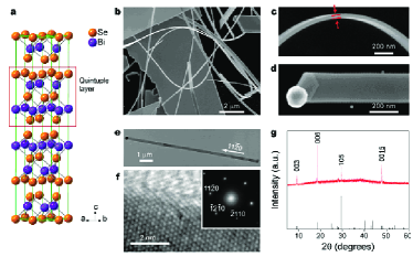
The contribution of the bulk carriers can be suppressed by reducing sample size. Quasi-1D nanoribbons, with their large surface-to-volume ratios, provide excellent geometries for probing the transport properties of surface states. In this work, single-crystalline Bi2Se3 nanoribbons are synthesized via a gold-catalyzed vapor-liquid-solid (VLS) growth 20Morales . The layered Bi2Se3 has a rhombohedral phase with the space group D53d (R-3m)21Wyckoff , and consists of planar, covalently bonded sheets linked predominantly by van der Waals interactions (Fig. 1a). Figure 1b shows a typical scanning electron microscopy (SEM) image of the as-grown Bi2Se3 nanoribbons with thicknesses of 25-100nm and widths ranging from 50nm to several micrometers. The nanoribbon has smooth sidewalls and flat surfaces (Fig. 1c). The presence of a gold nanoparticle at the end of each nanoribbon suggests the VLS growth mechanism, in which catalyst particles promote nucleation and unidirectional growth of layered structures (Figs 1d and 1e). Energy-dispersive X-ray spectroscopy (EDX) analysis reveals uniform chemical composition along the ribbon length with a Bi:Se atomic ratio of 2:3, indicating stoichiometric Bi2Se3 free of detectable impurities. The nanoribbons are single crystalline rhombohedral phase with atomically smooth edges, length along the [11-20] direction, and height parallel to the c-axis, as shown in transmission electron microscopy, the selected area electron diffraction pattern (Fig. 1f, inset), and the X-ray diffraction (XRD) pattern (Fig. 1g). By controlling the growth temperature, using Sn/Au alloy as the catalyst, or post-annealing in Se vapor, we are able to vary the electron density without changing the crystal structure. The total electron density measured by the Hall effect is between to cm-2, with an effective Hall mobility cm2/Vs extracted from the sheet resistance . Such a high electron density indicates the existence of bulk carriers in our nanoribbons, while their contribution is suppressed compared with macroscopic samples. Results reported below are only observed in samples with relatively low total density cm-2.

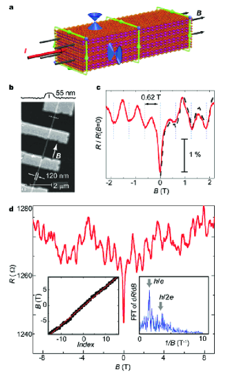
The quasi-1D narrow nanoribbons in Fig. 1e are model systems for studying the topological surface states. When an external magnetic field () is applied along the length of the nanoribbon, quantum interference effects will occur if the conduction electrons remain phase coherent after completing closed trajectories, each encircling a certain magnetic flux. For the bulk carriers, there exist various sample-specific, or more precisely, impurity-dependent loops, resulting in universal conductance fluctuations (UCF) 22Lee with aperiodic field dependence, commonly observed in small metallic and semiconducting structures. For the 2D states covering the entire surface, however, all phase coherent trajectories participating in the quantum interference enclose the same area perpendicular to the -field (Fig. 2a). The low temperature transport therefore exhibits periodic magnetoresistance oscillations, a hallmark of the well-known Aharonov-Bohm (AB) effect 23Aharonov , with a characteristic period of the external magnetic field , where is the flux quantum, the cross sectional area of the nanoribbon, the Planck’s constant and the electron charge, respectively.

To probe the quantum interference effect in the Bi2Se3 nanoribbons, we fabricated four-point probe devices by depositing Ti/Au Ohmic contacts. A representative device is shown in Fig. 2b, where the width and thickness of the ribbon are determined by SEM and AFM, respectively. The four-terminal magnetoresistance is measured in a 9-Tesla Quantum Design PPMS system with a base temperature of 2K. At low magnetic fields T, the weak anti-localization effect 24Hikami with a sharp cusp at zero field is seen in Fig. 2c, consistent with the presence of strong spin-orbit coupling in Bi2Se3. For fields 0.15T 2T, pronounced and reproducible resistance oscillations with a period of 0.62T are observed. For the AB effect, this period is associated with an area of m2, in excellent agreement with the measured cross sectional area of the nanoribbon m2 (Fig. 2b). At higher fields (Fig. 2d), the perfect periodicity deteriorates slightly, but a roughly linear relation of 0.6T per resistance minimum still holds up to 9T. As shown in the inset of Fig. 2d, the prominent oscillation and a weak second harmonic at are better seen by taking the fast Fourier transform (FFT) of the derivative d/d, a method commonly applied to separate the oscillatory part from slow-varying background 25Huber . The noisy background in the FFT spectrum and the deviation from pure periodicity at high fields are presumably due to the contribution from the bulk states, which superimpose aperiodic UCF onto the clean AB oscillations. We also note that SdH oscillations of the bulk electrons may be responsible for the slow-varying background seen in Fig. 2d. Since quantum confinement in the plane perpendicular to the field direction is not negligible, several electric sub-bands may form in our nanoribbons, and magnetic depopulation of these sub-bands would modify the usual relation at high Landau level fillings 26Berggren . Nevertheless, neither of these bulk-related effects could result in B-periodicity over the large field range in this experiment. Therefore, the AB effect in Bi2Se3 nanoribbons indisputably manifests the existence of the conducting surface states, which, based on theories and the ARPES data 10Zhang ; 11Xia , are highly exotic as opposed to the trivial surface inversion effect in certain semiconducting materials.
The observation of the AB oscillations in Bi2Se3 nanostructures provides important insights into the topological surface states. First of all, although a significant portion of the conduction is carried by the bulk states, the interaction between bulk and surface electrons does not destroy the phase coherence of the surface states. The oscillation amplitude observed in our experiment is on the order of the quantized conductance (), comparable to other quasi-1D nanostructures 25Huber and disordered metal cylinders 18Aronov . Since full revolution around the perimeter of the ribbon is required for the interference effect, our result demonstrates that the surface states not only exist on the top and bottom (0001) surfaces but also propagate coherently through the side walls of the nanoribbon. Given that the side surface is terminated with dangling bonds and adjacent quasi-2D layers are predominantly linked by van der Waals coupling, the coherent motion of the electrons through the side surface is highly nontrivial, providing further evidence for the topological robustness of the surface states. Finally, the primary oscillation period corresponds to the Aharonov-Bohm quantization, while the Altshuler-Aronov-Spivak (AAS) oscillation with period 27Altshuler ; 28Bachtold originating from weak (anti) localization is suppressed. The absence of the AAS effect, at least in the low magnetic field region, may be related to the distinct property of the topological surface states, i.e., electrons with opposite momentum have opposite spin polarization. For these states, back scattering events are forbidden for but are present for finite field strengths even if the flux of the field is an integer multiple of flux quanta. Consequently, the anti-localization behavior observed at is absent for other integer multiples of flux, leading to the suppression of the AAS effect.

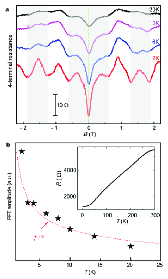
Further information about the AB effect can be obtained by the temperature evolution of the magnetoresistance oscillations. As shown in Fig. 3a, most oscillatory features persist up to 20K, beyond which the zero field resistance increases considerably (inset of Fig. 3b), presumably due to phonon scattering. Again, we take the FFT of dR/dB to analyze the T-dependence data. In Fig. 3b, the oscillation amplitude roughly scales with between 2K and 20K, where the inelastic phonon scattering is negligible. The same T-dependence was observed in mesoscopic metal rings and explained by the averaging of conduction channels in the absence of inelastic scattering 29Washburn . At high densities with weak electron-electron interaction, the phase-breaking time can be estimated from the thermal broadening of the Fermi-Dirac distribution, or . As a result, the oscillation amplitude scales with the phase coherent diffusion length , where is the diffusion constant, in accordance with the experimental data.

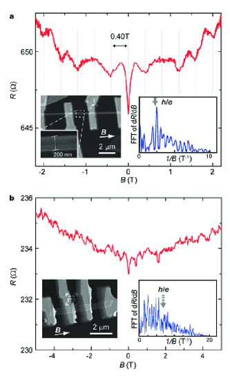
In the end, we briefly discuss the quantum interference effect in two more Bi2Se3 nanoribbon devices at 2K. For the relatively narrow ribbon in Fig. 4a, well defined resistance minima are observed at multiples of 0.4T except for weak shoulders at 0.8T. This period is better seen in the FFT plot. The inferred area from the flux quantization again matches the cross sectional area (200nm 50nm) well within the measurement error bars. On the other hand, the magnetoresistance of the wide ribbon (570nm 50nm) in Fig. 4b does not display obvious periodicity, and the characteristics of its Fourier spectrum are reminiscent of the UCF effect. In other words, neither the bulk nor the surface electrons can produce a coherent path that predominantly encloses a fixed amount of flux. Thus the phase coherent length in our nanoribbons is likely to be around 0.5m at 2K, consistent with an order-of-magnitude estimate from SdH measurements. Further experiments down to lower temperatures are expected to enhance for the observation of AB effects in wider ribbons and will be investigated in the future.
In conclusion, we have fabricated topological insulator materials in nanoribbon form, with large surface-to-volume ratios. We report the first transport measurement in this class of materials, based on the AB oscillations of the conductance associated with the topological surface states. The distribution of the AB periods provides the clear evidence to distinguish the surface conductance from the bulk, paving the way to eventually eliminate the bulk conduction.
References
- (1) B. A. Bernevig, T. L. Hughes, S. C. Zhang, Science 314, 1757 (2006).
- (2) B. A. Bernevig, S. C. Zhang, Phys. Rev. Lett. 96, 106802 (2006).
- (3) C. L. Kane, E. J. Mele, Phys. Rev. Lett. 95, 226801 (2005).
- (4) L. Fu, C. L. Kane, E. J. Mele, Phys. Rev. Lett. 98, 106803 (2007).
- (5) J. E. Moore, L. Balents, Phys. Rev. B 75, 121306 (2007).
- (6) X. L. Qi, T. L. Hughes, S. C. Zhang, Phys. Rev. B 78, 195424 (2008).
- (7) M. Konig et al., Science 318, 766 (2007).
- (8) D. Hsieh et al., Nature 452, 970 (2008).
- (9) D. Hsieh et al., Science 323, 919 (2009).
- (10) H. Zhang et al., Nat. Phys. 5, 438 (2009).
- (11) Y. Xia et al., Nat. Phys. 5, 398 (2009).
- (12) Y. L. Chen et al., Science, 325, 178 (2009).
- (13) S. K. Mishra, S. Satpathy, O. Jepsen, J. Phys. Cond. Mat. 9, 461 (1997).
- (14) X. L. Qi, R. D. Li, J. D. Zang, S. C. Zhang, Science 323, 1184 (2009).
- (15) L. Fu, C. L. Kane, Phys. Rev. Lett. 100, 096407 (2008).
- (16) L. Fu, C. L. Kane, Phys. Rev. B 76, 045302 (2007).
- (17) T. Ando, A. B. Fowler, F. Stern, Rev. Mod. Phys. 54, 437 (1982).
- (18) A. G. Aronov, Y. V. Sharvin, Rev. Mod. Phys. 59, 755 (1987).
- (19) H. Kohler, A. Fabricius, Phys. Stat. Solidi B 71, 487 (1975).
- (20) A. M. Morales, C. M. Lieber, Science 279, 208 (1998).
- (21) R. W. G. Wyckoff, Crystal Structures. (Krieger, 1986).
- (22) P. A. Lee, A. D. Stone, Phys. Rev. Lett. 55, 1622 (1985).
- (23) Y. Aharonov, D. Bohm, Phys. Rev. 115, 485 (1959).
- (24) S. Hikami, A. I. Larkin, Y. Nagaoka, Prog. Theo. Phys. 63, 707 (1980).
- (25) T. E. Huber, K. Celestine, M. J. Graf, Phys. Rev. B 67, 245317 (2003).
- (26) K. F. Berggren, T. J. Thornton, D. J. Newson, M. Pepper, Phys. Rev. Lett. 57, 1769 (1986).
- (27) B. L. Altshuler, A. G. Aronov, B. Z. Spivak, JETP Lett. 33, 94 (1981).
- (28) A. Bachtold et al., Nature 397, 673 (1999).
- (29) S. Washburn, C. P. Umbach, R. B. Laibowitz, R. A. Webb, Phys. Rev. B 32, 4789 (1985).