Conductance characteristics of current-carrying d-wave weak links
Abstract
The local quasiparticle density of states in the current-carrying d-wave superconducting structures was studied theoretically. The density of states can be accessed through the conductance of the scanning tunnelling microscope. Two particular situations were considered: the current state of the homogeneous film and the weak link between two current-carrying d-wave superconductors.
pacs:
74.50.+r, 74.78.-w, 74.78.Bz, 85.25.CpI Introduction
Unconventional superconductors exhibit different features interesting both from the fundamental point of view and for possible applications review(d-wave) . In particular, double degenerated state can be realized in d-wave Josephson junctions review(KOZ) . If the misorientation angle between the banks of the junction is taken , the energy minima of the system appear at the order parameter phase difference . These degenerate states correspond to the counter flowing currents along the junction boundary. Such characteristics make d-wave Josephson junctions interesting for applications, such as qubits dd-qubit . Our proposition was to make these qubits controllable with the externally injected along the boundary transport current KOSh04 . It was shown that the transport current and the spontaneous one do not add up – more complicated interference of the condensate wave functions takes place. This is related to the phenomena, known as the paramagnetic Meissner effect review(d-wave) .
It was demonstrated both experimentally Braunisch and theoretically Higashitani ; FRS97 that at the boundary of some high- superconductors placed in external magnetic field the current flows in the direction opposite to the diamagnetic Meissner supercurrent which screens the external magnetic field. This countercurrent is carried by the surface-induced quasiparticle states. These nonthermal quasiparticles appear because of the sign change of the order parameter along the reflected quasiparticle trajectory. Such a depairing mechanism is absent in the homogeneous situation. Note that in a homogeneous conventional superconductor at zero temperature the quasiparticles appear only when the Landau criterion is violated, at . Here is the superfluid velocity which parameterizes the current-carrying state, stands for the bulk order parameter, and is the Fermi momentum. The appearance of the countercurrent can be understood as the response of the weak link with negative self-inductance to the externally injected transport supercurrent. The state of the junction in the absence of the transport supercurrent at zero temperature is unstable at from the point of view that small deviations change the Josephson current from to its maximal value KO . The response of the Josephson junction to small transport supercurrent at produces the countercurrent Sh04 . It is similar to the equilibrium state with the persistent current in 1D normal metal ring with strong spin-orbit interaction: there is degeneracy at zero temperature and , and the response of the ring is different at or , where is the effective magnetic field which enters in the Hamiltonian through the Zeeman term (which breaks time-reversal symmetry) 1DNring . The degeneracy is lifted by small effective magnetic field so that the persistent current rapidly changes from to its maximum value. In the case of the weak link between two superconductors in the absence of the transport supercurrent there is degeneracy between and zero-energy states; both the time-reversal symmetry breaking by the surface (interface) order-parameter and the Doppler shift (due to the transport supercurrent or magnetic field) lift the degeneracy and result in the surface (interface) current Braunisch .
In recent years mesoscopic superconducting structures continue to attract attention because of the possible application as qubits, quantum detectors etc. (e.g. dd-qubit , Jtransistor ). In particular, such structures can be controlled by the transport supercurrent and the magnetic flux (through the phase difference on Josephson contact). This was in the focus of many recent publications, e.g. KOSh04 ; Rashedi04 ; Zhang04 ; Ngai05 ; Sh06 ; Lukic07 . Here we continue to study the mesoscopic current-carrying d-wave structures. Particularly, we study the impact of the transport supercurrent on the density of states in both homogeneous film and in the film which contains a weak link.
II Model and basic equations
We consider a perfect contact between two clean singlet superconductors. The external order parameter phase difference is assumed to drop at the contact plane at . The homogeneous supercurrent flows in the banks of the contact along the -axis, parallel to the boundary. The sample is assumed to be smaller than the London penetration depth so that the externally injected transport supercurrent can indeed be treated as homogeneous far from the weak link. The size of the weak link is assumed to be smaller than the coherence length. Such a system can be quantitatively described by the Eilenberger equation KO . Taking transport supercurrent into account leads to the Doppler shift of the energy variable by . The standard procedure of matching the solutions of the bulk Eilenberger equations at the boundary gives the Matsubara Green’s function at the contact at KOSh04 . Then for the component of , which defines both the current density and the density of states (see below), we obtain in the left () and right () banks of the junction:
| (1) |
| (2) |
| (3) |
Here are Matsubara frequencies, stands for the order parameter in the left (right) bank, and
| (4) |
The direction-dependent Doppler shift results in the modification of current-phase dependencies and in the appearance of the countercurrent along the boundary.
The function defines the current density, as following:
| (5) |
Here is the density of states at the Fermi level, denotes averaging over the directions of Fermi velocity , is the unit vector in the direction of .
Analytic continuation of , i.e.
| (6) |
gives the retarded Green’s function, which defines the density of states:
| (7) |
Here is the relaxation rate in the excitation spectrum of the superconductor.
The local density of states can be probed with the method of the tunnelling spectroscopy by measuring the tunnelling conductance of the contact between our superconducting structure and the normal metal scanning tunnelling microscope’s (STM) tip. At low temperature the dependence of the conductance on the bias voltage is given by the following relation Duke :
| (8) |
where is the conductance in the normal state; is the angle-dependent superconductor-insulator-normal metal barrier transmission probability. The barrier can be modelled e.g. as in Ref. FRS97 with the uniform probability within the acceptance cone , where is the polar angle and the small value of describes the thick tunnelling barrier:
| (9) |
where is the theta function.
III Conductance characteristics of the homogeneous current-carrying film
Before studying the current-carrying weak link we consider the homogeneous situation. We will consider the d-wave film as shown in the left inset in Fig. 1. The motivation behind this study is twofold: first, to demonstrate the application of the theory presented above, and second, to describe recent experimental results Ngai05 .
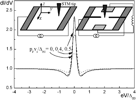
The system considered consists of the d-wave film, in which the current is injected along the -axis, and the STM normal metal tip (another STM contact is not shown in the scheme for simplicity; for details see Ngai05 ). Following the experimental work Ngai05 , we consider the -axis along the -axis and the misorientation angle between -axis and the direction of current (-axis) to be . Such problem can be described with the equations presented in the previous section as following FRS97 ; Sh06 .
Consider the specular reflection at the border, when the boundary between the current-carrying -wave superconductor and the insulator can be modelled as the contact between two superconductors with the order parameters given by and and with . Then from Eq. (3) we have the following:
| (10) |
where and . This expression is valid for any relative angle between the -axis and the normal to the boundary; in particular,
| (11) | |||||
| (12) |
The accurate dependence of the gap function can be obtained from Ref. KOSh04 with introducing as following: (which is analogous to Eq. (6)). The energy values in this paper are made dimensionless with the zero-temperature gap at zero current: .
And now with Eqs. (12) and (6-8) we plot the STM conductance for the current-carrying -wave film in Fig. (1). We obtain the suppression of the zero-bias conductance peak by the transport supercurrent, as was studied in much detail in Ref. Ngai05 . Our results are in agreement with their Fig. 1. Also the authors of Ref. Ngai05 developed the model based on phase fluctuations in the BTK formalism to explain the suppression of the zero-bias conductance peak. However, their theoretical result, Fig. 2, describes the experimental one only qualitatively, leaving several distinctions. They are the following: (i) position of the minima ( and for the experiment and the theory respectively); (ii) height of the zero-bias peak at zero transport current ( and respectively); (iii) height of the peak at maximal transport current ( and respectively); (iv) presence/absence of the minima for all curves. Our calculations, Fig. (1), demonstrate agreement with the experiment in all these features. The agreement we obtained with two fitting parameters, and .
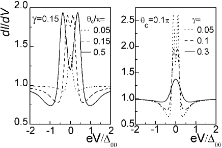
To further demonstrate the impact of the two fitting parameters of our model, and , in Fig. (2) we plot the normalized conductance fixing one of them and changing another. The figure clearly demonstrates how they change the shape of the curves: the position of the minima, splitting of the zero-bias peak etc. Note that the splitting is suppressed at small and high . This absence of the splitting was observed in the experiment Ngai05 and studied in several articles, e.g. Aubin .
IV Conductance characteristics of the current-carrying weak link
Consider now the weak link between two -wave current-carrying banks. For studying the effect of both the transport current and the phase difference on the density of states in the contact, we propose the scheme, presented in the right inset in Fig. 1. The supercurrent is injected along -axis in the superconducting film, as it was discussed in the previous section. Besides, the weak link is created by the impenetrable for electrons partition at . The small break in this partition () plays the role of the weak link in the form of the pinhole model KO ; FogYipKurk ; Sh06 . The STM tip in the scheme is positioned above the weak link to probe the density of states in it. Two more contacts along the -axis provide the order parameter phase difference along the weak link. This can be done, for example, by connecting the contacts with the inductance, as shown in the scheme, and applying magnetic flux to this inductance. Then one obtains the phase control of the contact with the relation: .
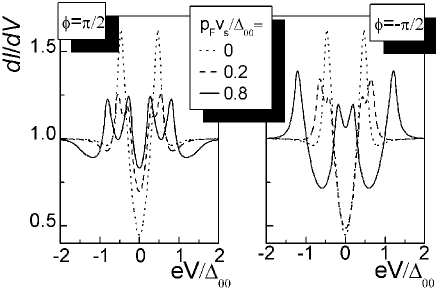
The two half-plains (for and ) play the role of the two banks of the contact, which we also call left and right superconductors. In our scheme the banks carry the transport current along the boundary, and the Josephson current along the contact is created due to the phase difference. The banks we consider to be -wave superconductors with -axis along the -axis and with the misorientation angles and . Now we can apply the equations presented in Sec. II to describe the conductance characteristics of the contact between current-carrying -wave superconductors. This is done in Fig. 3, where the normalized conductance is plotted for two values of the phase difference, for and with . The two values of the phase difference, , are particularly interesting for the application since they correspond to the double-degenerate states dd-qubit ; KOSh04 . So, the density of states is the same in the absence of the transport supercurrent in both panels in Fig. 3 with mid-gap states (at ) which create the spontaneous current along the boundary. The transport supercurrent () removes the degeneracy by significantly changing the mid-gap states (Fig. 3), which explains different dependencies of the current in the contact on the applied transport current (i.e. on ), studied in KOSh04 ; Sh04 .
V Conclusion
We have studied the density of states in the current-carrying -wave structures. Namely, we have considered, first, the homogeneous situation and, second, the superconducting film with the weak link. The former case was related to recent experimental work, while the latter is the proposition for the new one. The local density of states was assumed to be probed with the scanning tunnelling microscope. The density of states at the weak link and the current (i.e. its components through the contact and along the contact plane) are controlled by the values of and . The system is interesting because of possible applications: in the Josephson transistor with controlling parameters and governed by external magnetic flux and the transport supercurrent Jtransistor , and in solid-state qubits, based on a contact of -wave superconductors dd-qubit .
Acknowledgements.
The author is grateful to Yu.A. Kolesnichenko and A.N. Omelyanchouk for helpful discussions. This work was supported in part by the Fundamental Researches State Fund (grant number F28.2/019).References
- (1) C.C. Tsuei and J.R. Kirtley, Rev. Mod. Phys. 72, 969 (2000).
- (2) Yu.A. Kolesnichenko, A.N. Omelyanchouk, and A.M. Zagoskin, Fiz. Nizk. Temp. 30, 714 (2004) (Low Temp. Phys. 30, 535 (2004)).
- (3) A.M. Zagoskin, J. Phys.: Condens. Matter 9, L419 (1997); L.B. Ioffe et al., Nature 398, 679 (1999); A.M. Zagoskin, Turk. J. Phys. 27, 491 (2003).
- (4) Yu.A. Kolesnichenko, A.N. Omelyanchouk, and S.N. Shevchenko, Fiz. Nizk. Temp. 30, 288 (2004) (Low Temp. Phys. 30, 213 (2004)).
- (5) W. Braunisch, N. Knauf, V. Kateev, S. Neuhausen, A. Grutz, A. Koch, B. Roden, D. Khomskii, and D. Wohlleben, Phys. Rev. Lett. 68, 1908 (1992); H. Walter, W. Prusseit, R. Semerad, H. Kinder, W. Assmann, H. Huber, H. Burkhardt, D. Rainer, and J. A. Sauls, Phys. Rev. Lett. 80, 3598 (1998); E. Il’ichev, F. Tafuri, M. Grajcar, R.P.J. IJsselsteijn, J. Weber, F. Lombardi, and J.R. Kirtley, Phys. Rev. B 68, 014510 (2003).
- (6) S. Higashitani, J. Phys. Soc. Jpn. 66, 2556 (1997).
- (7) M. Fogelström, D. Rainer, and J.A. Sauls, Phys. Rev. Lett. 79, 281 (1997).
- (8) I.O. Kulik and A.N. Omelyanchouk, Fiz. Nizk. Temp. 4, 296 (1978) (Sov. J. Low Temp. Phys. 4, 142 (1978)).
- (9) Yu.A. Kolesnichenko, A.N. Omelyanchouk, and S.N. Shevchenko, Phys. Rev. B 67, 172504 (2003); S.N. Shevchenko, in Realizing Controllable Quantum States–In the Light of Quantum Computation, Proceedings of the International Symposium on Mesoscopic Superconductivity and Spintronics, Atsugi, Japan, edited by H. Takayanagi and J. Nitta, World Scientific, Singapore, p. 105 (2005); arXiv:cond-mat/0404738.
- (10) T.-Z.Qian, Y.-S. Yi, and Z.-B. Su, Phys. Rev. B 55, 4065 (1997); V.A. Cherkassky, S.N. Shevchenko, A.S. Rozhavsky, I.D. Vagner, Fiz. Nizk. Temp. 25, 725 (1999) (Low Temp. Phys. 25, 541 (1999)).
- (11) F.K. Wilhelm, G. Shön, and A.D. Zaikin, Phys. Rev. Lett. 81, 1682 (1998); E.V. Bezuglyi, V.S. Shumeiko, and G. Wendin, Phys. Rev. B 68, 134606 (2003).
- (12) G. Rashedi and Yu.A. Kolesnichenko, Phys. Rev. B 69, 024516 (2004).
- (13) D. Zhang, C.S. Ting, and C.-R. Hu, Phys. Rev. B 70, 172508 (2004).
- (14) J. Ngai, P. Morales, and J.Y.T. Wei, Phys. Rev. B 72, 054513 (2005).
- (15) S.N. Shevchenko, Phys. Rev. B 74, 172502 (2006).
- (16) V. Lukic and E.J. Nicol, Phys. Rev. B 76, 144508 (2007).
- (17) C. Duke, Tunneling in solids, Academic Press, NY (1969).
- (18) H. Aubin, L.H. Greene, S. Jian, and D.G. Hinks, Phys. Rev. Lett. 89, 177001 (2002).
- (19) M. Fogelström, S. Yip, and J. Kurkijärvi, Czech. J. Phys. 46, 1057 (1996).
- (20) G. Rashedi, J. Phys.: Condens. Matter 21, 075704 (2009).
- (21) A.N. Omelyanchouk, S.N. Shevchenko, and Yu.A. Kolesnichenko, J. Low Temp. Phys. 139, 247 (2005).