Predicted band structures of III-V semiconductors in wurtzite phase
Abstract
While non-nitride III-V semiconductors typically have a zincblende structure, they may also form wurtzite crystals under pressure or when grown as nanowhiskers. This makes electronic structure calculation difficult since the band structures of wurtzite III-V semiconductors are poorly characterized. We have calculated the electronic band structure for nine III-V semiconductors in the wurtzite phase using transferable empirical pseudopotentials including spin-orbit coupling. We find that all the materials have direct gaps. Our results differ significantly from earlier ab initio calculations, and where experimental results are available (InP, InAs and GaAs) our calculated band gaps are in good agreement. We tabulate energies, effective masses, and linear and cubic Dresselhaus zero-field spin-splitting coefficients for the zone-center states. The large zero-field spin-splitting coefficients we find may lead to new functionalities for designing devices that manipulate spin degrees of freedom.
pacs:
71.15.Dx, 71.20.-b, 71.00.00I Introduction
Semiconductor nanowhiskers (NW) have attracted a tremendous amount of interest in recent years Haraguchi et al. (1992); Hiruma et al. (1993); Ohlsson et al. (2001); Gutiérrez et al. (2001); Poole et al. (2003); Regolin et al. (2007); Jabeen et al. (2009); Colombo et al. (2008). Much of it is due to their potential application in areas such as photovoltaic cellsHu and Chen (2007); Tsakalakos et al. (2007); Czaban et al. (2009), nano-electromechanical resonator arrays Henry et al. (2007), microwave and THz detection Balocco et al. (2005); Gustavsson et al. (2008), single photon detectionRosfjord et al. (2006); Zinoni et al. (2007); Dauler et al. (2007), field-effectCui et al. (2003)Greytak et al. (2004) and single-electron transistorsThelander et al. (2003), and various other electronic and optoelectronic devices Björk et al. (2002, 2002); Panev et al. (2003); Duan et al. (2001); Samuelson et al. (2004). NWs are also interesting because 1D systems can be made using material combinations for which large lattice mismatches prohibit quantum well structures, allowing greater freedom in material combinations for device engineering.
In contrast to bulk non-nitride III-V materials which are usually zincblende (ZB), NWs predominantly crystalize in the wurtzite (WZ) phase Koguchi et al. (1992); Mattila et al. (2006); Tomioka et al. (2007). Several different theoretical explanations for this behavior have been proposed. Recent calculations suggest that the WZ phase is energetically favorable for small NW radii Akiyama et al. (2006); Galicka et al. (2008), although this does not account for all NW radii for which the WZ phase is experimentally observed. Calculations based on an empirical nucleation model indicate that WZ formation is favored for certain ranges of the interface energiesGlas et al. (2007). Ab initio calculations indicate that the WZ phase is favored due to the accumulation of electrons at the interstitial site containing the Au catalyst Haneda et al. (2008), while other calculations show that the polytype is determined by growth kineticsDubrovskii and Sibirev (2008). It should be noted that these different mechanisms are not necessarily mutually exclusive.
Theoretical understanding of the electronic and optical properties of semiconductor nanostructures is based on a knowledge of the electronic properties of bulk materials. However little is known about the electronic band structure of III-V semiconductors in WZ phase since most do not naturally occur as bulk crystals. Moreover, the NWs often contain sections of ZB material, forming heterostructures out of the differing band structures of the two polytypesHiruma et al. (1993); Xiong et al. (2006); Bao et al. (2008); Soshnikov et al. (2005). Band structures of WZ III-V semiconductors have been calculated using density functional theory (DFT) in the local density approximation (LDA)Murayama and Nakayama (1994); Yeh et al. (1994a). Since the LDA underestimates band gaps the WZ band structure can not be directly determined, and instead calculations of WZ and ZB are typically compared to obtain the differences between the two polytypes. The band structures of GaAs and InAs in WZ phase have also been calculated using the GW methodZanolli et al. (2007a), giving somewhat different results than those from the LDA. In addition to the inherent errors in ab initio band gaps, all of the above calculations neglected the spin-orbit coupling, which is known to significantly alter the valence band structure of semiconductors.
In this paper we present calculations of the bulk electronic band structures of the nine non-nitride III-V semiconductors in WZ phase using empirical pseudopotentials including spin-orbit coupling. These calculations are based on transferable model pseudopotentials assuming ideal WZ structure. The spherically symmetric ionic model potentials are first obtained by fitting the calculated bulk ZB energies to experimental energies at high symmetry points. The band structure of the WZ polytype is then obtained by transferring the model pseudopotentials to the WZ pseudopotential Hamiltonian using the appropriate crystal structure factors.
This method has been proven to be very successful in obtaining the bulk band structures of semiconductor polytypesBergstresser and Cohen (1967); Joannopoulos and Cohen (1973); Foley and Tansley (1986); Bandić and Ikonić (1995); Pugh et al. (1999); Pennington and Goldsman (2001); Fritsch et al. (2003, 2006); Cohen and Chelikowsky (1988). The anion and cation pseudopotentials are specific to each material and are only transfered between polytypes. Therefore the model potentials should be transferable between ZB and WZ polytypes due to the similarities in their crystal structures. In both structures all of the nearest neighbors and nine out of the twelve second nearest neighbors are at identical crystallographic locations Birman (1959a) while the the second nearest neighbors are equidistant.
This paper is organized as follows. In section II we outline the similarities and differences between ZB and WZ crystal structures as well as the direct correspondence between high symmetry -points in the two polytypes. In section III we describe the transferable pseudopotential method. In section IV we present the calculated band structures, their respective density of states (DOS), and effective masses. Finally, we summarize the results in section VI.
II Wurtzite vs Zincblende
II.1 Crystal Structure
The ZB crystal is formed by two interpenetrating face centered cubic (FCC) Bravais lattices (each of a different atomic species), whereas the WZ structure is constructed from two interpenetrating hexagonal close-packed (HCP) lattices. The differences between the two structures are best understood by viewing along the [111] direction (Fig. 1a,b), along which both look like stacked hexagonal layers. The atoms are identical within each layer, and the layers alternate between the anion and the cation. For the ideal WZ crystal the lattice constant is given by and the lattice constant along the -axis (axis perpendicular to the hexagon) is related to the in-plane lattice constant by . Since the WZ crystal is tetrahedral, the nearest neighbors are the same in the two polytypes. In addition, we see from Fig. 1 that nine of the twelve nearest neighbors in WZ are the same as in ZB. These structural similarities suggest that the local electronic environment will be the same in the two crystals, and therefore the crystal potentials will be nearly identical in WZ and ZB.
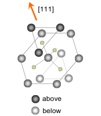
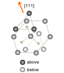
In WZ the type-1 atoms are located at and , while the type-2 atoms are located at and , where the primitive lattice vectors are , and . The parameter for the ideal WZ crystal structure, which we will assume throughout this paper. This assumption is supported by the fact that experiments show that WZ GaAs is very close to idealMcMahon and Nelmes (2005).
II.2 Band Structure
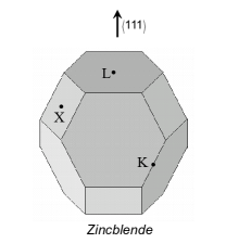
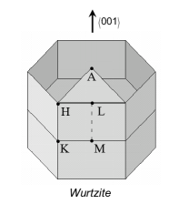
Due to the similarities of the two crystals, many of the high symmetry points in the Brillouin zones of ZB and WZ are related to each other, and an understanding of their correspondences is useful for understanding trends in the band structures of the two polytypes. Fig. 2 shows the relationships among the zone center states in WZ and the corresponding and points in ZB, both with and without spin-orbit coupling. One of the most important features is that in the empty lattice approximation the L-point in ZB is zone-folded to the -point in WZ. As a result, in the absence of spin-orbit coupling, the , and states in ZB correspond to , and respectively in WZ (Fig. 2). Because of this folding over of the -valley, indirect gap ZB materials with an valley conduction band minimum would be expected to have a direct gap in the ZB phase unless the energy of the state was significantly shifted by the crystal potential.
ind
The states at the top of the valence band in WZ also have some important differences with their ZB counterparts. In the absence of spin-orbit coupling, the hexagonal crystal field of WZ splits the -like state of ZB into a four-fold degenerate and a doubly degenerate . In terms of the -orbitals, these states are are . With the inclusion of spin-orbit coupling, splits into the heavy-hole and the light-hole. Therefore, all zone center states in WZ belong to either , , or . There are similar correspondences between the high symmetry directions of the two crystals. The symmetry line ) in ZB corresponds to the line in WZBirman (1959a).
II.3 Spin Splitting
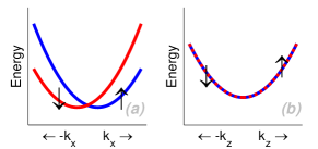
For certain individual states in crystals lacking inversion symmetry, spin-orbit coupling causes a splitting of spin-up and spin-down states which leads to ( see Fig. 3). The states at are still two-fold degenerate, resulting in a nonvanishing at the origin for certain crystallographic directions. In the case of WZ, the states remain spin-degenerate for along the -axis because at any point along the direction (), the crystallographic point group is Casella (1959). As all the irreducible representations compatible with spin () in this group are doubly-degenerateKoster et al. (1963), there is no spin-splitting along .
In WZ, the spin splitting effects near zone center can be described with an effective one band Hamiltonian Casella (1960); Hopfield and Thomas (1961); Lew Yan Voon et al. (1996)
| (1) |
where are constants. This effective Hamiltonian is invariant with respect to for all odd powers of . The coefficients of the linear and cubic Dresselhaus spin-splitting terms can be obtained by expanding Eq. 1 up to . Near the crossing, the difference in energies between the spin-split bands in Fig. 3(a) has the form Lew Yan Voon et al. (1996)
| (2) |
where and are the linear and cubic Dresselhaus spin-splitting coefficients respectively for band . These coefficient characterize the spin spin splitting, and may be determined from the computed band structure by fitting a function of the above form. While the existence of a spin splitting in a particular direction is determined by symmetry considerationsCasella (1959), the magnitude can vary considerably. Although both ZB and WZ crystals lack inversion symmetry, spin splitting effects are much more prominent in WZ due to its lower crystal symmetry Birman (1959b); Hopfield (1961); Adler (1962); K. H mmer (1978); I. Broser (1979); Koteles and Winterling (1980); Shigenari et al. (1984); Lew Yan Voon et al. (1996); Culcer et al. (2005); Wang et al. (2007); Goano et al. (2007); Fu and Wu (2008), which can be of particular use in spintronic devices.
III Method
III.1 Pseudopotentials
Our band structures are computed using the empirical pseudopotential method of Cohen and Chelikowsky Cohen and Chelikowsky (1988) with a model potential applicable to both ZB and WZ structures. Pseudopotentials exploit the fact that the electronic wave function may be separated into the sum of a rapidly oscillating part near the atomic cores and a slowly varying piece. The pseudopotential approach relies on the assumption that the core electrons are frozen and that the valence electrons move in a weak single-electron potential making the true atomic wave function orthogonal to the core states. The pseudo wave equation is then
| (3) |
where is the smoothly varying pseudo wave function, and is the pseudopotential which includes a repulsive core to partially cancel the deep potential near the atomic corePhillips and Kleinman (1959). By taking to be a local pseudopotential which is a function only of position, it may be expanded in terms of reciprocal lattice vectors, , as
| (4) | |||||
| (5) |
where labels the atom type, is the form factor, is the structure factor, is the number of atoms per unit cell of type , and is the position of atom number of type .
For binary compounds it is convenient to separate the pseudopotential into symmetric (S) and antisymmetric (A) parts as
| (6) | |||||
The symmetric and antisymmetric structure factors are given by
| (7) | |||||
| (8) |
where is the number of atoms per unit cell and for one type of atom and for the other type. The symmetric and antisymmetric form factors, and , are obtained from the sum and difference of the spherically symmetric anion and cation potentials.
There are several approaches to calculating Cohen and Chelikowsky (1988); Ehrenreich et al. (1970). In the empirical pseudopotential approach used here, and are adjusted to fit the calculated energy spectrum to experimentally determined energies at band extrema. Model potentials that yield an accurate band structure of a known polytype should reliably predict the band structure for the unknown polytype if the two crystal structures are similar. To compute the WZ band structure using pseudopotentials obtained from ZB requires and to be continuous functions that can be evaluated at any value of . A wide variety model potentials have been usedEhrenreich et al. (1970); Xia (1988); Yeh et al. (1994b); Pugh et al. (1999); Fan et al. (2006) and we use potentials of the form
| (9) | |||||
| (10) |
where , and the parameters and are obtained for each material by fitting to the ZB band structure.
III.2 Spin-Orbit Interactions
We include the spin-orbit coupling, given by
| (11) |
using the method of WeiszWeisz (1966). Eq. 11 cannot be used directly since spin-orbit coupling involve the core states which are omitted from the pseudo wave equation as a result of orthogonalization. Instead, by returning to the original Schrödinger equation we may expand in terms of the core states to obtain Weisz (1966); Saravia and Brust (1968)
| (12) |
In this way the matrix elements of for core states may be parameterized and then fit to experiment in the same way as the pseudopotential form factors. By expanding in Bloch functions, and expressing the core states in terms of its constituent atomic radial wave functions and respective spherical harmonics, Eq. 12 can be recast as Weisz (1966)
where is the derivative of the Legendre polynomial, s are the Pauli matrices, , and is the angle between and . The coefficient is given in terms of the core wave functions by
| (14) |
| (15) |
where is a normalization constant such that approaches unity in the limit goes to zero and is the principal quantum number for the core state being considered. For III-V semiconductors, it is not required to expand Eq. LABEL:SOC1 beyond since they do not have core shells filled beyond -orbitals. Expanding Eq. LABEL:SOC1 up to , the matrix elements for the spin-orbit coupling in a binary compound are
| (16) |
| (17) | |||||
| (18) | |||||
| (19) | |||||
| (20) |
where the superscript (1),(2) specifies which atom, the coefficient is an empirically adjusted parameter and is the ratio of the anion to cation spin-orbit splitting energies for a given core stateChelikowsky and Cohen (1976). The overlap integral, , is constructed from the atomic core wave functions using Eq. 15. The radial part of the core wave function, , is an approximate Hartree-Fock solution taken from Herman-Skillman tablesHerman and Skillman (1963). For Ga, In, As and Sb, terms up to in Eq. 16 are included while Al and P only go up to since they do not have valence d-shells. With the inclusion of Eq. 16 the total pseudopotential Hamiltonian becomes
| (21) |
III.3 Fitting
The pseudopotential parameters , , and in Eqs. 9 and 10 were determined by fitting the band structure obtained from the Hamiltonian of Eq. 21 to experimental energies of the band extrema of ZB materials. The Hamiltonian was evaluated in a plane wave basis with a cutoff of , and for each value of the Hamiltonian was diagonalized to give energies to be fit to the experimental target values. The fitting was accomplished by minimizing the error function
| (22) |
where the sum over ranges over the targeted energies , and are weighting factors adjusted to speed convergence. Seven energies were used as fitting parameters, (all with respect to ): . The targeted values of , , and were taken from Ref. Vurgaftman et al., 2001 while the higher transition energies, were taken from Ref. Madelung, 2004. In addition constraints were imposed to ensure the correct band ordering of valence states by forcing the third and fourth (spin-degenerate) valence band states to have symmetry. was minimized with respect to , , and using Powell’s method, with the local pseudopotential form factors from Ref. Cohen and Bergstresser, 1966 used as an initial starting point. Slightly different initial values were used as a check that the solution did not converge to a spurious local minimum since Powell’s method finds the local minimum. In those cases where the value of was large, indicating a poor fit, the weights were adjusted to climb out of the local minimum in which the algorithm was trapped, and the minimization algorithm was continued.
III.4 Transferable Pseudopotentials
Once the form factors have been determined for the ZB polytype, they may be transfered to the WZ structure by centering the spherically symmetric atomic pseudopotentials on the positions of the ions in the WZ form. The transferability depends on the similarities of the crystal structures, and for sufficiently dissimilar polytypes one would expect the method to fail. Fortunately, as discussed in section II.1 ZB and WZ are very similar, as the WZ crystal structure can be thought of as a variation of ZB with the same local structure, but a slightly different long range structure. It is important to note that all the parameters were fit independently for each material, and the pseudopotentials were transferred between polytypes with the same binary composition. Since the WZ primitive cell has four atoms (rather than the two of ZB), its structure factor contain more terms. Substituting the atomic positions in section II.1 into Eqs. 7 and 8 the WZ structure factors are
| (23) | |||
| (24) |
where () are the components of the reciprocal lattice vector .
IV Results
IV.1 Calculated III-V Zinc Blende band structures
The pseudopotential parameters determined by fitting to the zincblende band structures are given in Table 1, including the spin-orbit parameters. The accuracy of the results may be gauged by Table 2, which gives the ratio of each band energy to the experimental value to which it was fitVurgaftman et al. (2001). We see that the results agree with experiment to within for all but . Even for , the deviation from the experimental value is greater than only for InSb. We have also made a similar comparison of the effective masses and Luttinger parametersVurgaftman et al. (2001). These values differ from the energy ratios in that the masses were not fit to experimental data. The masses were determined by doing a quadratic fit to the band extremum, with the Luttinger parameters determined from
| (25) |
It should be noted that several of the masses listed in Ref. Vurgaftman et al., 2001 are either obtained theoretically or have large experimental uncertainties. For example, only theoretically calculated effective masses are available for AlP and for the valence band of AlSb. To the best of our knowledge, experimental results are not available for these compounds. In the case of GaP the conduction band effective mass is extrapolated from its ternary alloy. For InAs, there is great experimental uncertainty about the heavy and light hole masses Vurgaftman et al. (2001). Even though we have omitted nonlocal corrections not associated with spin-orbit coupling, our effective masses are in very good agreement for compounds containing lighter elements.
| Material | ||||||||||
|---|---|---|---|---|---|---|---|---|---|---|
| AlP | 0.083 | -0.579 | 0.031 | -2.586 | -0.11 | 0.9 | -0.061 | -1.178 | 0.012 | 0 |
| AlAs | 0.062 | -0.459 | 0.027 | -2.629 | -0.041 | 1.003 | -0.056 | -1.693 | ||
| AlSb | 0.06 | -0.412 | 0.032 | -2.548 | -0.09 | 0.17 | -0.051 | -2.098 | ||
| GaP | 0.085 | -0.457 | 0.04 | -2.566 | -0.351 | 5.165 | -0.205 | 0.339 | 0.385 | |
| GaAs | 0.058 | -0.467 | 0.023 | -2.583 | -0.063 | 1.091 | -0.074 | -1.298 | 0.052 | |
| GaSb | 0.042 | -0.343 | 0.022 | -2.584 | -0.009 | 0.618 | -0.043 | -2.233 | 0.056 | |
| InP | 0.049 | -0.385 | 0.027 | -2.602 | 0 | 0.847 | -0.059 | -1.654 | 0.243 | |
| InAs | 0.036 | -0.298 | 0.033 | -2.615 | -0.011 | 1.359 | -0.121 | -1.124 | 0.082 | |
| InSb | 0.022 | -0.174 | 0.023 | -2.42 | -0.012 | 1.158 | -0.082 | -1.363 | 0.085 |
| Material | |||||||||||||
|---|---|---|---|---|---|---|---|---|---|---|---|---|---|
| AlP | 1.00 | 1.00 | 1.00 | 1.00 | - | - | - | 1.03 | 0.72 | 1.06 | 0.92 | 0.99 | 0.95 |
| AlAs | 1.00 | 1.00 | 1.01 | 1.00 | 1.01 | 1.01 | 1.00 | 0.99 | 0.99 | 1.07 | 0.95 | 0.84 | 0.96 |
| AlSb | 1.00 | 1.00 | 1.00 | 1.00 | 1.00 | 1.00 | 1.00 | 0.97 | 1.04 | 1.30 | 0.67 | 0.66 | 0.70 |
| GaP | 1.00 | 1.00 | 1.00 | 1.00 | 1.00 | 1.00 | 1.00 | 0.97 | 1.00 | 1.02 | 0.96 | 1.66 | 1.20 |
| GaAs | 1.00 | 1.00 | 1.00 | 1.00 | 1.00 | 1.00 | 1.00 | 0.95 | 1.16 | 1.19 | 0.81 | 0.90 | 0.83 |
| GaSb | 1.00 | 1.00 | 1.01 | 1.00 | 1.00 | 1.00 | 1.00 | 0.94 | 1.47 | 1.56 | 0.63 | 0.61 | 0.62 |
| InP | 1.00 | 1.00 | 1.00 | 1.00 | 1.00 | 1.00 | 1.00 | 1.02 | 1.08 | 1.03 | 0.96 | 0.98 | 1.00 |
| InAs | 1.00 | 1.00 | 1.00 | 1.01 | 1.00 | 1.00 | 1.00 | 0.95 | 1.36 | 1.05 | 0.61 | 0.60 | 0.62 |
| InSb | 1.00 | 1.00 | 1.01 | 1.00 | 1.00 | 1.00 | 1.00 | 0.84 | 1.85 | 1.73 | 0.55 | 0.54 | 0.56 |
IV.2 Predicted III-V Wurtzite band structures
The calculated band structure and the corresponding density of states(DOS) for each of the nine III-V semiconductors in WZ phase are shown in Fig. 4-12. The electronic band structures are calculated in the irreducible wedge of the Brillouin zone (Fig. 1(d)). It should be noted that the band structure of WZ is more complicated than that of ZB due to it lower crystal symmetry and has roughly twice as many bands over a given energy range. The irreducible representations of the zone center states was determined by transforming the pseudo wave functions under the symmetry operations of the respective crystallographic point group.
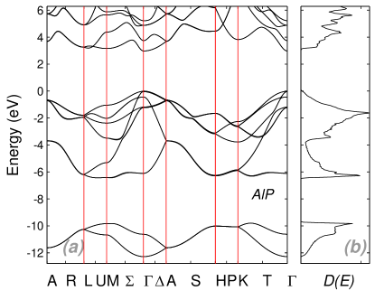
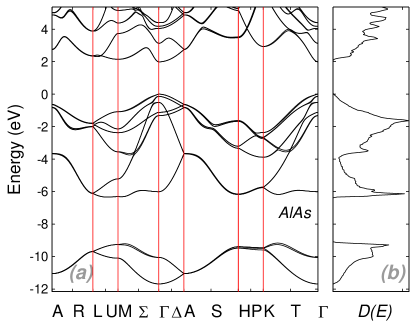
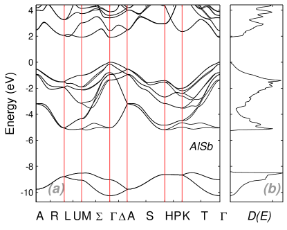
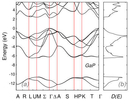
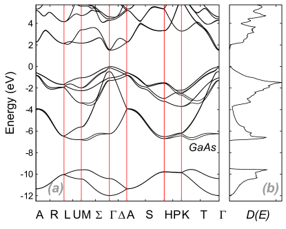
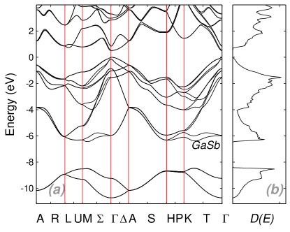
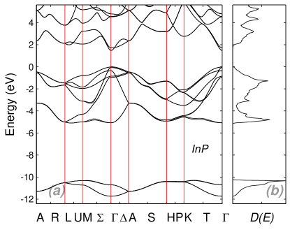
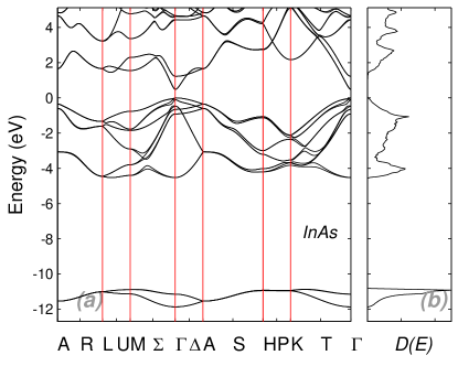
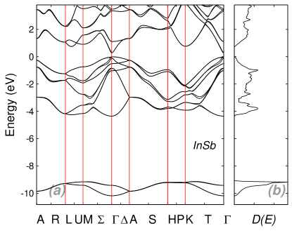
Tables 3-5 list the calculated zone center energies of the band extrema, effective masses for parallel and perpendicular to the axis, and the linear and cubic Dresselhaus spin splitting coefficients and . We calculated the Dresselhaus coefficients by fitting a function of the above form in Eq. 2 to the calculated band structures. These parameters may be used in constructing WZ Hamiltonians for nanostructure calculations Foley and Tansley (1986); Chuang and Chang (1996); Yeo et al. (1998); Sirenko et al. (1997); Xia and Li (1999); Mireles and Ulloa (2000); Rodina and Meyer (2001); Beresford (2004). We have also complied a summary (Table 6) listing the energy differences most important for nanostructures.
Foremost is the band gap and the irreducible representation of the conduction band minimum. In our calculations it is seen that all of the materials containing Al or Ga have conduction band minima in the WZ phase, whereas all of the materials containing In have conduction band minima. We also give the spin-orbit energy, , the crystal field splitting, , and the offset between the valence band edge of each polytypes. and are extracted using the quasi cubic approximation which assumes WZ to be equivalent to -strained ZB Bir and Pikus (1974); Chuang and Chang (1996), with and related to the hole energies by
| (26) |
where is a parameter relating the lattice constants, . For the ideal WZ structure assumed here, and is for an ideal WZ structure.
In ZB phase, AlP, AlAs, AlSb and GaP are indirect gap semiconductors with their conduction band minima ordered , , . Our calculations show that in all of the indirect gap ZB semiconductors become direct gap WZ materials with conduction band minima. Previous LDA calculations obtained indirect gaps for AlP and AlAs in WZ phase, with the conduction band minimum at Yeh et al. (1994a); Murayama and Nakayama (1994). Although this is not the case in our results, we do find the valley conduction band minimum only slightly above the minima (182 meV for AlP and 157 meV for AlAs). The same LDA calculations also predicted AlSb and GaP to have conduction band minima, in agreement with our resultsMurayama and Nakayama (1994). The direct gaps of AlP and AlSb in WZ phase are larger than the indirect (-valley) gaps of their respective ZB counterparts. Whereas the direct () gaps of AlAs and GaP in WZ phase are smaller than the indirect gaps of their ZB counterparts.
Although GaAs and GaSb have direct gaps in the ZB phase, for both materials the zone-folded valley in WZ is lower, giving a minimum. For WZ, GaAs has a band gap () which is only slightly smaller than that of its ZB polytype, while GaSb has a significantly smaller gap () in WZ phase. In both cases this is due to being close to . This behavior is most apparent for GaSb, hence our prediction for GaSb is consistent with that of Ref. Yeh et al., 1994a and Ref. Murayama and Nakayama, 1994. In light of recent experimental results, the case of WZ GaAs will be discussed in greater detail below. All three Indium containing compounds InP, InAs and InSb are direct gap semiconductors in WZ phase with conduction band minima and have higher band gaps than their respective direct gap ZB polytypes.
While little is known about the WZ polytypes, experimental data is available for the band gaps of GaAs, InAs and InP. Table (7) compares our calculated band gaps for these three materials to experiment and ab initio calculations. We have only tabulated their SX and GW results as they make different qualitative predictions as to whether the band gap of WZ GaAs is larger or smaller than for ZB. Note that the values listed for the ab initio methods are not listed directly in the respective references. As none of the directly obtained gaps from ab initio calculations are correct, the values are obtained from the experimental ZB gap and the calculated percentage change between the two polytypes. As can be seen, our results are in very good agreement with experiments. More importantly, they are in agreement with the experimental trends as to whether the WZ band gap is larger or smaller than the ZB gap. This is most apparent in the case of GaAs, for which ab initio calculations (except the SX methodZanolli et al. (2007b)) predict that GaAs should have a larger direct band gap in WZ phase than in ZB, in disagreement with experiment. All of the low temperature experimental results show that for GaAs the WZ phase has a smaller band gap than ZB. In addition, the experimental gaps are obtained from photoluminescence measurements on GaAs nanowires, which will be slightly larger due to confinement.
In the case of InP our results are in agreement with experiments as well as with the trends from LDA calculations. Photocurrent spectroscopy measurements on nanowires have been extrapolated in to obtain a band gap for InP of Trägaardh et al. (2007), which is higher than valules from photoluminescence measurements. The fact that the measured values are higher than our pseudopotential calculations may be du to confinement effects in the nanowire experiments. Our calculated gap for InP is also in good agreement with the calculations of Zanolli et al. Zanolli et al. (2007b).
| AlP | AlAs | AlSb | |||||||||||||||
|---|---|---|---|---|---|---|---|---|---|---|---|---|---|---|---|---|---|
| -12.368 | 1.351 | 1.365 | 0.000 | -22.061 | -11.763 | 1.307 | 1.318 | 0.000 | -28.806 | -10.299 | 1.405 | 1.424 | 0.001 | -164.203 | |||
| -10.710 | 0.550 | 1.598 | 0.001 | -0.019 | -10.131 | 0.502 | 1.512 | 0.113 | -0.143 | -9.078 | 0.629 | 1.820 | 0.021 | -0.186 | |||
| -6.195 | 0.298 | 4.002 | 0.038 | 0.115 | -6.088 | 0.280 | 3.246 | 0.004 | 0.256 | -5.090 | 0.319 | 2.357 | 0.296 | 1.485 | |||
| -1.249 | 1.655 | 0.299 | 0.074 | 23.745 | -1.341 | 1.608 | 0.257 | 0.164 | 8.293 | -1.377 | 1.611 | 0.284 | 0.577 | 16.066 | |||
| -1.200 | 1.662 | 0.296 | 0.000 | 24.557 | -1.131 | 1.658 | 0.235 | 0.000 | 9.896 | -0.955 | 1.667 | 0.202 | 0.000 | 10.236 | |||
| -0.435 | 0.145 | 1.260 | 0.047 | -11.829 | -0.518 | 0.150 | 0.837 | 0.140 | -59.309 | -0.802 | 0.237 | 0.971 | 0.095 | -234.420 | |||
| -0.044 | 0.931 | 0.253 | 0.052 | 25.634 | -0.139 | 0.478 | 0.259 | 0.236 | -7.256 | -0.156 | 0.220 | 0.373 | 0.125 | 17.954 | |||
| 0.000 | 0.972 | 0.248 | 0.000 | 25.032 | 0.000 | 0.933 | 0.216 | 0.000 | 10.703 | 0.000 | 0.959 | 0.211 | 0.000 | 11.064 | |||
| 2.969 | 1.187 | 0.170 | 0.034 | -1.069 | 1.971 | 1.081 | 0.142 | 0.027 | 0.635 | 1.891 | 1.160 | 0.157 | 0.209 | -10.332 | |||
| 3.775 | 0.182 | 0.157 | 0.003 | -17.969 | 3.153 | 0.180 | 0.141 | 0.004 | 76.350 | 2.418 | 0.163 | 0.143 | 0.005 | 14.487 | |||
| 4.822 | 0.924 | 2.729 | 0.017 | 26.128 | 3.993 | 0.883 | 4.253 | 0.104 | 6.743 | 3.384 | 1.155 | 1.549 | 0.054 | 16.784 | |||
| 4.831 | 0.923 | 2.652 | 0.000 | 28.017 | 4.133 | 0.857 | 5.281 | 0.000 | 31.568 | 3.577 | 1.149 | 3.279 | 0.000 | 23.544 | |||
| 5.193 | 2.263 | 0.409 | 0.018 | -36.548 | 4.360 | 2.806 | 0.484 | 0.219 | -67.663 | 3.872 | 3.705 | 0.551 | 0.210 | -67.883 | |||
| GaP | GaAs | GaSb | |||||||||||||||
|---|---|---|---|---|---|---|---|---|---|---|---|---|---|---|---|---|---|
| -12.942 | 1.391 | 1.400 | 0.000 | -10.751 | -12.033 | 1.339 | 1.350 | 0.000 | -28.285 | -10.757 | 1.270 | 1.288 | 0.000 | -58.903 | |||
| -11.369 | 0.615 | 1.768 | 0.076 | -0.070 | -10.452 | 0.533 | 1.520 | 0.003 | -0.089 | -9.269 | 0.452 | 1.453 | 0.028 | -0.301 | |||
| -6.313 | 0.312 | 2.362 | 0.064 | 0.003 | -6.289 | 0.291 | 12.730 | 0.188 | 0.467 | -5.992 | 0.261 | 3.827 | 0.344 | 1.577 | |||
| -1.327 | 1.577 | 0.242 | 0.105 | 18.694 | -1.291 | 1.698 | 0.242 | 0.440 | 31.168 | -1.537 | 1.535 | 0.193 | 1.137 | 25.843 | |||
| -1.233 | 1.624 | 0.238 | 0.000 | 21.321 | -1.049 | 1.745 | 0.224 | 0.000 | 42.790 | -1.030 | 1.604 | 0.131 | 0.000 | 77.808 | |||
| -0.373 | 0.118 | 1.145 | 0.068 | 26.433 | -0.475 | 0.118 | 0.434 | 0.048 | 141.143 | -0.874 | 0.149 | 0.436 | 0.147 | -141.671 | |||
| -0.050 | 0.821 | 0.210 | 0.072 | 35.712 | -0.120 | 0.200 | 0.197 | 0.067 | 67.513 | -0.142 | 0.086 | 0.192 | 0.175 | 23.793 | |||
| 0.000 | 0.941 | 0.205 | 0.000 | 29.339 | 0.000 | 1.026 | 0.134 | 0.000 | 36.419 | 0.000 | 0.833 | 0.087 | 0.000 | 73.448 | |||
| 2.251 | 1.162 | 0.143 | 0.075 | -3.725 | 1.503 | 1.050 | 0.125 | 0.212 | -12.750 | 0.509 | 0.983 | 0.096 | 0.716 | -72.842 | |||
| 2.877 | 0.153 | 0.125 | 0.006 | 53.344 | 1.588 | 0.090 | 0.082 | 0.037 | -55.218 | 0.851 | 0.064 | 0.060 | 0.034 | -33.327 | |||
| 4.395 | 1.135 | 1.665 | 0.076 | 15.714 | 4.271 | 0.861 | 1.977 | 0.355 | 62.864 | 2.824 | 0.857 | 1.225 | 0.184 | 71.733 | |||
| 4.429 | 1.233 | 1.872 | 0.000 | 9.533 | 4.417 | 0.793 | 0.722 | 0.000 | 123.206 | 2.970 | 0.785 | 0.695 | 0.000 | 57.196 | |||
| 4.940 | 1.510 | 0.608 | 0.004 | -76.564 | 4.575 | 0.974 | 0.317 | 0.337 | -282.988 | 3.284 | 0.394 | 0.470 | 0.262 | -283.959 | |||
| InP | InAs | InSb | |||||||||||||||
|---|---|---|---|---|---|---|---|---|---|---|---|---|---|---|---|---|---|
| -11.746 | 1.660 | 1.677 | 0.000 | -28.484 | -11.875 | 2.071 | 2.034 | 0.001 | -30.395 | -10.181 | 1.802 | 1.778 | 0.001 | -40.757 | |||
| -10.711 | 0.936 | 2.509 | 0.036 | -0.038 | -11.151 | 1.397 | 3.377 | 0.034 | -0.116 | -9.421 | 1.094 | 2.932 | 0.043 | -0.155 | |||
| -5.091 | 0.390 | 1.845 | 0.087 | 0.223 | -4.526 | 0.469 | 1.349 | 0.088 | 0.248 | -4.351 | 0.420 | 1.244 | 0.004 | -0.317 | |||
| -0.949 | 1.833 | 0.237 | 0.011 | 3.746 | -0.910 | 2.116 | 0.210 | 0.078 | 5.879 | -1.021 | 2.185 | 0.222 | 0.188 | 2.114 | |||
| -0.849 | 1.894 | 0.230 | 0.000 | 2.693 | -0.652 | 2.164 | 0.166 | 0.000 | 27.849 | -0.847 | 0.203 | 0.210 | 0.595 | 633.586 | |||
| -0.348 | 0.097 | 1.205 | 0.074 | 97.187 | -0.469 | 0.115 | 0.319 | 0.849 | 744.548 | -0.508 | 2.310 | 0.206 | 0.000 | 7.028 | |||
| -0.063 | 0.839 | 0.169 | 0.084 | 65.030 | -0.105 | 0.101 | 0.113 | 1.414 | 648.740 | -0.098 | 0.058 | 0.094 | 1.812 | 178.644 | |||
| 0.000 | 1.273 | 0.158 | 0.000 | 45.639 | 0.000 | 1.700 | 0.084 | 0.000 | 1107.720 | 0.000 | 2.060 | 0.066 | 0.000 | 2450.059 | |||
| 1.474 | 0.105 | 0.088 | 0.011 | -54.015 | 0.481 | 0.060 | 0.042 | 0.571 | -1143.621 | 0.287 | 0.051 | 0.035 | 1.212 | -2955.560 | |||
| 1.712 | 1.094 | 0.132 | 0.032 | -1.600 | 1.222 | 1.276 | 0.113 | 0.007 | -1.456 | 1.116 | 1.781 | 0.118 | 0.197 | -11.492 | |||
| 4.535 | 1.646 | 0.952 | 0.097 | 70.102 | 4.445 | 3.377 | 0.255 | 0.790 | -106.736 | 3.395 | 1.785 | 2.105 | 1.909 | -44.165 | |||
| 4.575 | 1.701 | 0.845 | 0.000 | 95.004 | 4.631 | 2.025 | 0.059 | 0.791 | -2927.150 | 3.513 | 0.656 | 1.635 | 1.987 | 42.178 | |||
| 4.802 | 0.804 | 0.448 | 0.158 | -98.388 | 4.662 | 2.580 | 0.052 | 0.000 | 2824.700 | 3.930 | 0.565 | 2.502 | 0.000 | 38.729 | |||
| (eV) | (eV) | (eV) | (eV) | |
|---|---|---|---|---|
| AlP | 0.070 | 0.409 | -0.1428 | |
| AlAs | 0.319 | 0.338 | -0.0841 | |
| AlSb | 0.683 | 0.276 | -0.0909 | |
| GaP | 0.082 | 0.341 | -0.0801 | |
| GaAs | 0.351 | 0.244 | -0.0632 | |
| GaSb | 0.777 | 0.239 | -0.1186 | |
| InP | 0.108 | 0.303 | -0.0646 | |
| InAs | 0.379 | 0.195 | 0.0405 | |
| InSb | 0.787 | 0.159 | 0.0872 |
| (eV) Present Calculations | (eV) Ab initio Methods | (eV) Experiment | |
|---|---|---|---|
| GaAs | 1.623[Yeh et al. (1994a), 1.6Murayama and Nakayama (1994), 1.381Zanolli et al. (2007b)a,1.811Zanolli et al. (2007b)b | 1.498Haraguchi et al. (1994),1.476Soshnikov et al. (2006),1.494Regolin et al. (2007),1.51Khorenko et al. (2004) | |
| InP | 1.5403Murayama and Nakayama (1994) | 1.44Mattila et al. (2007),1.452Reitzenstein et al. (2007),1.49Mishra et al. (2007),1.508Ding et al. (2007),1.645Trägaardh et al. (2007) | |
| InAs | 0.6424Murayama and Nakayama (1994), 0.47Zanolli et al. (2007b) | 0.54Trägaardh et al. (2007) |
The spin-orbit coupling can alter the ordering of the valence band states in different WZ semiconductors. For example, in CdS and CdSe the top three valence states are in descending order , , (referred to as normal ordering)Birman (1959b); Thomas and Hopfield (1959) while in ZnO the ordering is , , (anomalous ordering) which results from a negative spin-orbit energy. In our calculations, all materials except InSb have normal ordering. In the case of InSb the ordering of the valence band states is complicated by its very large spin-orbit splitting which forces the split-off hole bellow the next state (which comes from the ’folded over’ -like -valley states in ZB). This results in the unusual , , , ordering of valence band states in InSb.
Tables 3-5 also give the Dresselhaus coefficients for each band. As expectedLew Yan Voon et al. (1996), all states have zero linear Dresselhaus coefficients () while all and states have nonzero linear and cubic spin-splitting coefficients. Amongst the five WZ phase semiconductors with the largest spin-orbit energies (), InSb has the largest Dresselhaus coefficients, followed by GaSb, InAs, GaAs and AlSb.
V Summary
We have calculated the electronic band structure for nine III-V semiconductors in WZ phase using empirical pseudopotentials with the inclusion of spin-orbit coupling. The predicted band structures are based on the concept of transferable model potentials. Our calculations show that in WZ phase, InP, InAs and InSb have a direct gap () which is larger than the corresponding zincblende material. AlP, AlAs, AlSb, GaP, GaAs and GaSb also have direct gaps, but with conduction band minima. WZ AlP and AlAs have larger direct gaps than the indirect gaps of their ZB polytypes. The opposite trend is seen in AlSb and GaP which have smaller direct gaps than their indirect gaps in ZB phase. In WZ phase GaAs and GaSb have direct gaps which are smaller than their ZB counterparts.
Our calculations are in excellent agreement with with experimentally obtained band gaps for GaAs, InAs and InP in WZ phase. Significantly, our results agree with experiment over whether the WZ band gap is larger or smaller than the ZB gap, in contrast to ab initio methods. We have extracted the linear and cubic Dresselhaus spin-splitting coefficients and find they are generally, though not always, larger for materials with larger spin-orbit coupling. The relatively large spin-splittings may be of use for spin-dependent transport in WZ nanowires. More recently, the WZ phase of GaAs has been grown in bulkMcMahon and Nelmes (2005). More experimental measurements on such bulk WZ phase III-V semiconductors, would lead to a clearer understanding of their electronic properties.
VI Acknowledgements
We would like to acknowledge support from the University of Iowa.
References
- Haraguchi et al. (1992) K. Haraguchi, T. Katsuyama, K. Hiruma, and K. Ogawa, Appl. Phys. Lett. 60, 745 (1992).
- Hiruma et al. (1993) K. Hiruma, M. Yazawa, K. Haraguchi, K. Ogawa, T. Katsuyama, M. Koguchi, and H. Kakibayashi, J. Appl. Phys. 74, 3162 (1993).
- Ohlsson et al. (2001) B. J. Ohlsson, M. T. Björk, M. H. Magnusson, K. Deppert, L. Samuelson, and L. R. Wallenberg, Appl. Phys. Lett. 79, 3335 (2001).
- Gutiérrez et al. (2001) H. R. Gutiérrez, M. A. Cotta, and M. M. G. de Carvalho, Appl. Phys. Lett. 79, 3854 (2001).
- Poole et al. (2003) P. J. Poole, J. Lefebvre, and J. Fraser, Appl. Phys. Lett. 83, 2055 (2003).
- Regolin et al. (2007) I. Regolin, V. Khorenko, W. Prost, F. J. Tegude, D. Sudfeld, J. Kästner, G. Dumpich, K. Hitzbleck, and H. Wiggers, J. Appl. Phys. 101, 054318 (pages 5) (2007).
- Jabeen et al. (2009) F. Jabeen, S. Rubini, and F. Martelli, Microelectronics Journal 40, 442 (2009).
- Colombo et al. (2008) C. Colombo, D. Spirkoska, M. Frimmer, G. Abstreiter, and A. F. i Morral, Phys. Rev. B 77, 155326 (pages 5) (2008).
- Hu and Chen (2007) L. Hu and G. Chen, Nano Lett. 7, 3249 (2007).
- Tsakalakos et al. (2007) L. Tsakalakos, J. Balch, J. Fronheiser, B. A. Korevaar, O. Sulima, and J. Rand, Appl. Phys. Lett. 91, 233117 (pages 3) (2007).
- Czaban et al. (2009) J. A. Czaban, D. A. Thompson, and R. R. LaPierre, Nano Lett. 9, 148 (2009).
- Henry et al. (2007) T. Henry, K. Kim, Z. Ren, C. Yerino, J. Han, and H. X. Tang, Nano Lett. 7, 3315 (2007).
- Balocco et al. (2005) C. Balocco, A. M. Song, M. Aberg, A. Forchel, T. Gonzalez, J. Mateos, I. Maximov, M. Missous, A. A. Rezazadeh, J. Saijets, et al., Nano Lett. 5, 1423 (2005).
- Gustavsson et al. (2008) S. Gustavsson, I. Shorubalko, R. Leturcq, T. Ihn, K. Ensslin, and S. Schön, Phys. Rev. B 78, 035324 (pages 7) (2008).
- Rosfjord et al. (2006) K. M. Rosfjord, J. K. W. Yang, E. A. Dauler, A. J. Kerman, V. Anant, B. M. Voronov, G. N. Gol’tsman, and K. K. Berggren, Opt. Express 14, 527 (2006).
- Zinoni et al. (2007) C. Zinoni, B. Alloing, L. H. Li, F. Marsili, A. Fiore, L. Lunghi, A. Gerardino, Y. B. Vakhtomin, K. V. Smirnov, and G. N. Gol’tsman, Appl. Phys. Lett. 91, 031106 (pages 3) (2007).
- Dauler et al. (2007) E. Dauler, B. Robinson, A. Kerman, J. Yang, E. Rosfjord, V. Anant, B. Voronov, G. Gol’tsman, and K. Berggren, Applied Superconductivity, IEEE Transactions on 17, 279 (2007), ISSN 1051-8223.
- Cui et al. (2003) Y. Cui, Z. Zhong, D. Wang, W. U. Wang, and C. M. Lieber, Nano Lett. 3, 149 (2003).
- Greytak et al. (2004) A. B. Greytak, L. J. Lauhon, M. S. Gudiksen, and C. M. Lieber, Appl. Phys. Lett. 84, 4176 (2004).
- Thelander et al. (2003) C. Thelander, T. M. rtensson, M. T. Björk, B. J. Ohlsson, M. W. Larsson, L. R. Wallenberg, and L. Samuelson, Appl. Phys. Lett. 83, 2052 (2003).
- Björk et al. (2002) M. T. Björk, B. Ohlsson, T. Sass, A. Persson, C. Thelander, M. Magnusson, K. Deppert, L. R. Wallenberg, and L. Samuelson, Appl. Phys. Lett. 80, 1058 (2002).
- Björk et al. (2002) M. T. Björk, B. J. Ohlsson, C. Thelander, A. I. Persson, K. Deppert, L. R. Wallenberg, and L. Samuelson, Appl. Phys. Lett. 81, 4458 (2002).
- Panev et al. (2003) N. Panev, A. I. Persson, N. Sköld, and L. Samuelson, Appl. Phys. Lett. 83, 2238 (2003).
- Duan et al. (2001) X. Duan, Y. Huang, Y. Cui, J. Wang, and C. M. Lieber, Nature (London) 409, 66 (2001).
- Samuelson et al. (2004) L. Samuelson, C. Thelander, M. T. Bj rk, M. Borgstr m, K. Deppert, K. A. Dick, A. E. Hansen, T. M rtensson, N. Panev, A. I. Persson, et al., Physica E 25, 313 (2004), ISSN 1386-9477, proceedings of the 13th International Winterschool on New Developments in Solid State Physics - Low-Dimensional Systems.
- Koguchi et al. (1992) M. Koguchi, H. Kakibayashi, M. Yazawa, K. Hiruma, and T. Katsuyama, Jpn. J. Appl. Phys. 31, 2061 (1992).
- Mattila et al. (2006) M. Mattila, T. Hakkarainen, M. Mulot, and H. Lipsanen, Nanotechnology 17, 1580 (2006).
- Tomioka et al. (2007) K. Tomioka, J. Motohisa, S. Hara, and T. Fukui, Jpn. J. Appl. Phys. 46, L1102 (2007).
- Akiyama et al. (2006) T. Akiyama, K. Nakamura, and T. Ito, Phys. Rev. B 73, 235308 (2006).
- Galicka et al. (2008) M. Galicka, M. Bukala, R. Buczko, and P. Kacman, Journal of Physics: Condensed Matter 20, 454226 (2008).
- Glas et al. (2007) F. Glas, J.-C. Harmand, and G. Patriarche, Phys. Rev. Lett. 99, 146101 (2007).
- Haneda et al. (2008) Y. Haneda, T. Akiyama, K. Nakamura, and T. Ito, Applied Surface Science 254, 7746 (2008), ISSN 0169-4332, 9th International Conference on Atomically Controlled Surfaces, Interfaces and Nanostructures 2007 (ASCIN-9).
- Dubrovskii and Sibirev (2008) V. G. Dubrovskii and N. V. Sibirev, Phys. Rev. B 77, 035414 (2008).
- Xiong et al. (2006) Q. Xiong, J. Wang, and P. C. Eklund, Nano Lett. 6, 2736 (2006).
- Bao et al. (2008) J. Bao, D. C. Bell, F. Capasso, J. B. Wagner, T. M̴rtensson, J. Tr ?g̴rdh, and L. Samuelson, Nano Lett. 8, 836 (2008).
- Soshnikov et al. (2005) I. P. Soshnikov, G. . Cirlin, A. A. Tonkikh, Y. B. Samsonenko, V. G. Dubovskii, V. M. Ustinov, O. M. Gorbenko, D. Litvinov, and D. Gerthsen, Physics of the Solid State 47, 2213 (2005).
- Murayama and Nakayama (1994) M. Murayama and T. Nakayama, Phys. Rev. B 49, 4710 (1994).
- Yeh et al. (1994a) C.-Y. Yeh, S.-H. Wei, and A. Zunger, Phys. Rev. B 50, 2715 (1994a).
- Zanolli et al. (2007a) Z. Zanolli, M.-E. Pistol, L. E. Froberg, and L. Samuelson, J Phys-Condens Mat 19, 295219 (2007a).
- Bergstresser and Cohen (1967) T. K. Bergstresser and M. L. Cohen, Phys. Rev. 164, 1069 (1967).
- Joannopoulos and Cohen (1973) J. D. Joannopoulos and M. L. Cohen, Phys. Rev. B 8, 2733 (1973).
- Foley and Tansley (1986) C. P. Foley and T. L. Tansley, Phys. Rev. B 33, 1430 (1986).
- Bandić and Ikonić (1995) Z. Z. Bandić and Z. Ikonić, Phys. Rev. B 51, 9806 (1995).
- Pugh et al. (1999) S. K. Pugh, D. J. Dugdale, S. Brand, and R. A. Abram, J. Appl. Phys. 86, 3768 (1999).
- Pennington and Goldsman (2001) G. Pennington and N. Goldsman, Phys. Rev. B 64, 045104 (2001).
- Fritsch et al. (2003) D. Fritsch, H. Schmidt, and M. Grundmann, Phys. Rev. B 67, 235205 (2003).
- Fritsch et al. (2006) D. Fritsch, H. Schmidt, and M. Grundmann, Appl. Phys. Lett. 88, 134104 (2006).
- Cohen and Chelikowsky (1988) M. Cohen and J. R. Chelikowsky, Electronic Structure and Optical Properties of Semiconductors (Springer, Berlin, 1988).
- Birman (1959a) J. L. Birman, Phys. Rev. Lett. 2, 157 (1959a).
- McMahon and Nelmes (2005) M. I. McMahon and R. J. Nelmes, Phys. Rev. Lett. 95, 215505 (2005).
- Casella (1959) R. C. Casella, Phys. Rev. 114, 1514 (1959).
- Koster et al. (1963) G. F. Koster, J. O. Dimmock, R. G. Wheeler, and H. Statz, The Properties of the Thirty-Two Point Groups (MIT Press, 1963).
- Casella (1960) R. C. Casella, Phys. Rev. Lett. 5, 371 (1960).
- Hopfield and Thomas (1961) J. J. Hopfield and D. G. Thomas, Phys. Rev. 122, 35 (1961).
- Lew Yan Voon et al. (1996) L. C. Lew Yan Voon, M. Willatzen, M. Cardona, and N. E. Christensen, Phys. Rev. B 53, 10703 (1996).
- Birman (1959b) J. L. Birman, Phys. Rev. 114, 1490 (1959b).
- Hopfield (1961) J. J. Hopfield, J. Appl. Phys. 32, 2277 (1961).
- Adler (1962) S. L. Adler, Phys. Rev. 126, 118 (1962).
- K. H mmer (1978) M. B. K. H mmer, R. Helbig, Phys. Stat. Sol. (b) 86, 527 (1978).
- I. Broser (1979) M. R. I. Broser, Phys. Stat. Sol. (b) 95, 141 (1979).
- Koteles and Winterling (1980) E. S. Koteles and G. Winterling, Phys. Rev. Lett. 44, 948 (1980).
- Shigenari et al. (1984) T. Shigenari, X. Z. Lu, and H. Z. Cummins, Phys. Rev. B 30, 1962 (1984).
- Culcer et al. (2005) D. Culcer, Y. Yao, A. H. MacDonald, and Q. Niu, Phys. Rev. B 72, 045215 (2005).
- Wang et al. (2007) W.-T. Wang, C. L. Wu, S. F. Tsay, M. H. Gau, I. Lo, H. F. Kao, D. J. Jang, J.-C. Chiang, M.-E. Lee, Y.-C. Chang, et al., Appl. Phys. Lett. 91, 082110 (pages 3) (2007).
- Goano et al. (2007) M. Goano, F. Bertazzi, M. Penna, and E. Bellotti, J. Appl. Phys. 102, 083709 (pages 11) (2007).
- Fu and Wu (2008) J. Y. Fu and M. W. Wu, J. Appl. Phys. 104, 093712 (pages 7) (2008).
- Phillips and Kleinman (1959) J. C. Phillips and L. Kleinman, Phys. Rev. 116, 287 (1959).
- Ehrenreich et al. (1970) H. Ehrenreich, F. Seitz, and D. Turnbull, eds., Solid State Physics: Advances in Research and Application, vol. 24 (Academic Press, NY and London, 1970).
- Xia (1988) J.-B. Xia, Phys. Rev. B 38, 8358 (1988).
- Yeh et al. (1994b) C.-Y. Yeh, S. B. Zhang, and A. Zunger, Phys. Rev. B 50, 14405 (1994b).
- Fan et al. (2006) W. J. Fan, J. B. Xia, P. A. Agus, S. T. Tan, S. F. Yu, and X. W. Sun, Journal of Applied Physics 99, 013702 (pages 4) (2006).
- Weisz (1966) G. Weisz, Phys. Rev. 149, 504 (1966).
- Saravia and Brust (1968) L. R. Saravia and D. Brust, Phys. Rev. 176, 915 (1968).
- Chelikowsky and Cohen (1976) J. R. Chelikowsky and M. L. Cohen, Phys. Rev. B 14, 556 (1976).
- Herman and Skillman (1963) F. Herman and S. Skillman, Atomic Structure Calculations (Prentice-Hall, Englewood Cliffs, N. J., 1963).
- Vurgaftman et al. (2001) I. Vurgaftman, J. R. Meyer, and L. R. Ram-Mohan, J. Appl. Phys. 89, 5815 (2001).
- Madelung (2004) O. Madelung, ed., Semiconductors Data Handbook (Springer-Verlag, Berlin Heidelberg New York, 2004), ed.
- Cohen and Bergstresser (1966) M. L. Cohen and T. K. Bergstresser, Phys. Rev. 141, 789 (1966).
- Chuang and Chang (1996) S. L. Chuang and C. S. Chang, Phys. Rev. B 54, 2491 (1996).
- Yeo et al. (1998) Y. C. Yeo, T. C. Chong, and M. F. Li, Journal of Applied Physics 83, 1429 (1998).
- Sirenko et al. (1997) A. A. Sirenko, T. Ruf, M. Cardona, D. R. Yakovlev, W. Ossau, A. Waag, and G. Landwehr, Phys. Rev. B 56, 2114 (1997).
- Xia and Li (1999) J.-B. Xia and J. Li, Phys. Rev. B 60, 11540 (1999).
- Mireles and Ulloa (2000) F. Mireles and S. E. Ulloa, Phys. Rev. B 62, 2562 (2000).
- Rodina and Meyer (2001) A. V. Rodina and B. K. Meyer, Phys. Rev. B 64, 245209 (2001).
- Beresford (2004) R. Beresford, J. Appl. Phys. 95, 6216 (2004).
- Bir and Pikus (1974) G. L. Bir and G. E. Pikus, Symmetry and strain-induced effects in semiconductors (Halsted, Jerusalem, 1974).
- Zanolli et al. (2007b) Z. Zanolli, F. Fuchs, J. Furthmueller, U. von Barth, and F. Bechstedt, Physical Review B 75, 245121 (2007b).
- Trägaardh et al. (2007) J. Trägaardh, A. I. Persson, J. B. Wagner, D. Hessman, and L. Samuelson, J. Appl. Phys. 101, 123701 (2007).
- Thomas and Hopfield (1959) D. G. Thomas and J. J. Hopfield, Phys. Rev. 116, 573 (1959).
- Haraguchi et al. (1994) K. Haraguchi, T. Katsuyama, and K. Hiruma, J. Appl. Phys. 75, 4220 (1994).
- Soshnikov et al. (2006) I. Soshnikov, G. Cirlin, V. Dubrovskii, A. Veretekha, A. Gladyshev, and V. Ustinov, Physics of the Solid State 48, 786 (2006).
- Khorenko et al. (2004) V. Khorenko, I. Regolin, S. Neumann, W. Prost, F.-J. Tegude, and H. Wiggers, Appl. Phys. Lett. 85, 6407 (2004).
- Mattila et al. (2007) M. Mattila, T. Hakkarainen, H. Lipsanen, H. Jiang, and E. I. Kauppinen, Appl. Phys. Lett. 90, 033101 (pages 3) (2007).
- Reitzenstein et al. (2007) S. Reitzenstein, S. Münch, C. Hofmann, A. Forchel, S. Crankshaw, L. C. Chuang, M. Moewe, and C. Chang-Hasnain, Appl. Phys. Lett. 91, 091103 (pages 3) (2007).
- Mishra et al. (2007) A. Mishra, L. V. Titova, T. B. Hoang, H. E. Jackson, L. M. Smith, J. M. Yarrison-Rice, Y. Kim, H. J. Joyce, Q. Gao, H. H. Tan, et al., Appl. Phys. Lett. 91, 263104 (pages 3) (2007).
- Ding et al. (2007) Y. Ding, J. Motohisa, B. Hua, S. Hara, and T. Fukui, Nano Lett. 7, 3598 (2007).