For further information contact Chao-Lin Kuo, e-mail: clkuo@stanford.edu
Antenna-Coupled TES Bolometer Arrays for CMB Polarimetry
Abstract
We describe the design and performance of polarization selective antenna-coupled TES arrays that will be used in several upcoming Cosmic Microwave Background (CMB) experiments: SPIDER, BICEP-2/SPUD. The fully lithographic polarimeter arrays utilize planar phased-antennas for collimation (F/4 beam) and microstrip filters for band definition (25% bandwidth). These devices demonstrate high optical efficiency, excellent beam shapes, and well-defined spectral bands. The dual-polarization antennas provide well-matched beams and low cross polarization response, both important for high-fidelity polarization measurements. These devices have so far been developed for the 100 GHz and 150 GHz bands, two premier millimeter-wave atmospheric windows for CMB observations. In the near future, the flexible microstrip-coupled architecture can provide photon noise-limited detection for the entire frequency range of the CMBPOL mission. This paper is a summary of the progress we have made since the 2006 SPIE meeting in Orlando, FL.
keywords:
cosmic microwave background, polarization, millimeter wave instrumentation1 Introduction
The primary science goals of CMB cosmology in the next decade are the degree-scale B-mode polarization induced by a gravitational wave background and the arcminute-scale B-mode induced by weak gravitational lensing from the large scale structures. The former will provide invaluable information on Inflation and early universe, while the latter offers a sensitive and complementary probe of the dark energy and the neutrino mass. To achieve these challenging goals, the instruments will require a large number of sensitive mm-wave detectors, wide frequency coverage for astronomical foreground monitoring, and exquisite control of polarization systematics[1].
Bolometers can provide photon noise-limited sensitivity over a wide frequency range. In the past few years many groups have been working to improve the scalability of bolometric polarimeters over the existing feedhorn-coupled micromesh bolometers[2]. These various efforts were surveyed in the NASA CMB Taskforce report in 2005 [1]. On the detector end, a very promising approach is the microstrip-coupled superconducting transition edge sensors (TES), with microstrip inline filters to define science bands [3, 4, 5]. The migration from semiconductor bolometers to TES bolometers enables the readout of thousands of pixels with moderate electronics complexity. This is achieved by superconducting quantum interference device (SQUID) multiplexers [6, 7], now a mature technology. In addition, the thermally active components (the bolometers) do not scale with the wavelengths in a microstrip-coupled architecture, therefore the entire frequency range ( 30 GHz to 500 GHz) of interest in CMB science can be covered by the same technology.
Because of these advantages, microstrip-coupled TES has been the technology of choice for the majority of the bolometer groups. However, different groups approach the beam formation problem differently: hemispherical silicon lenses [3], corrugated feed arrays from stacked metal platelets [4], and metalized micromachined silicon frontend are all being pursued. The CMB polarimeter described in this paper is based on planar slot-antenna arrays [5]. The signal is summed coherently by a network of niobium microstrips to synthesize a collimated beam. The key advantage for this approach is that the detector array is completely lithographic. The only add-on piece is a thin, flat quartz wafer for anti-reflection coating. This greatly reduces the fabrication complexity and cost, and allows for very high focal-plane packing density. The monolithic arrays are immune to differential thermal contraction and misalignment.
Co-locating dual-polarization detection is another key feature of the detectors described here. Bolometric receivers heavily rely on differencing to measure polarization. It is highly advantageous to measure orthogonal polarizations simultaneously with beams that are as well-matched as possible. So far, the most successful bolometric polarization experiments all take advantage of co-locating dual-polarization bolometers [8, 9, 10].
In SPIE 2006, we reported the performance of a series of prototype planar antenna-coupled TES detectors [5]. These first generation detectors provide good beam/band definition and demonstrate the feasibility of this technology. However their performance was not adequate for CMB applications. Since then we have made a lot of progress in the design and fabrication. The major improvements are: (1) A better dual-polarization antenna design that has over 30% bandwidth and intrinsically low cross-polarization and instrumental polarization (beam mismatch); (2) A new inter-layer dielectric material (SiO2) and deposition process (voltage-biased sputtering) that allows for better step coverage of the microstrips; and finally, (3) replacing the contact masks with stepping lithography, greatly improving the overall precision and accuracy of the structures over the large array area. After these improvements, the new detectors routinely achieve high polarization efficiency (97-99%), high optical efficiency (70%), and sufficient bandwidth (30%). These characteristics are comparable or better than the polarization sensitive detectors used in BICEP[9], QUAD[10], and Planck.
This paper is organized as follows. We first describe the architecture of a dual-polarization antenna-coupled bolometer in §2. The fabrication, measured optical properties, and array performance are presented in §3. We describe several CMB polarization experiments that will be using this technology and future development plans in §4.
2 A Lithographic Polarimeter
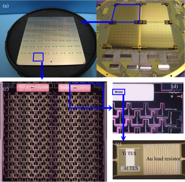
Figure 1 shows the overall structure of the focal plane arrays and the relative scales of various components. A polarimeter unit consists of an array of slot antennas, summing networks, band-defining filters, and the TES bolometers, described below.
2.1 Dual-polarization slot antennas
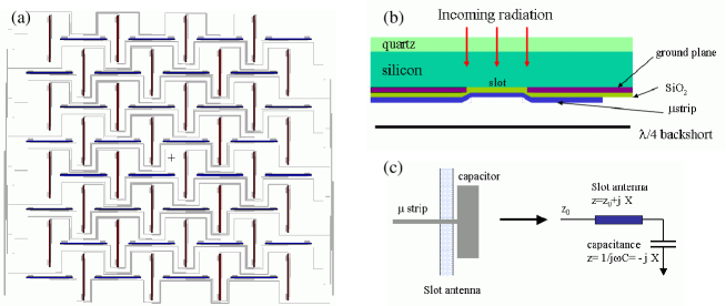
A collimated beam limits the radiation background onto the bolometer, and reduces side-lobes, stray light coupling, and susceptibility to cryogenic temperature fluctuations. Feed-coupled bolometers are especially advantageous compared to bare arrays under low background loading conditions at millimeter wave frequencies [11]. In an antenna-coupled detector, a planar array of slot antennas perform the function of beam collimation. The signals coming from the sub-antennas are combined coherently by a microstrip summing network to form a beam. The beam width is approximately given by , where is the linear dimension of the antenna and the wavelength in vacuum (Figure 2a).
Long slots in a ground plane are intrinsically polarization sensitive since microwave radiation tends to excite electric fields across the slots. Another key motivation for choosing a slot architecture is that most of the substrate remains metalized, shielding the summing network from the incoming radiation. The cross section of the antenna structure is shown in Figure 2(b). As mentioned earlier, we seek a design that provides co-locating dual-polarization detection and enough bandwidth (30%). These requirements are not easy to meet simultaneously, because periodic slot structures are intrinsically narrow banded, and usually pose significant challenge for implementaing the summing network. The first generation dual-polarization detectors reported in our previous paper [5] either produce excessive cross-polar response or span only 15-20% bandwidth.
After several iterations we arrived at the design shown schematically in Figure 2(a). The design has two sets of orthogonal slots, readout by two independent microstrip networks. Each slot is offset-fed to provide the appropriate impedance for the microstrip. This is done symmetrically on both ends of the slot to ensure low cross-polarization response. The interleaved structure allows for longer slots and sufficient gaps to accommodate the summing networks. The offset-feeding scheme produces significant reactance (), which is compensated by an appropriate coupling capacitor (Figure 2 c) to match the largely real impedance of the microstrip feed lines. Method of moment and HFSS calculations show that this antenna has over 35% bandwidth.
Dual-polarization antennas make efficient use of the focal plane real estate, and more importantly, reduce polarization artifacts associated with differencing and pointing errors [1]. From Figure 2(a) it is apparent that in our design the vertical and horizontal slots transform into each other after the device undergoes a rotation around the array center. In other words, the “dipole” components of beam mismatch vanishes [12, 1, 10] by design. The detailed antenna parameters and impedance calculation will be published elsewhere [13].
2.2 The summing networks
The signals from the sub-antennas are combined in phase by a superconducting niobium (Nb) microstrip network and transmitted to the TES. Two independent networks are required, one for each linear polarization. The sidelobe response of the antenna is determined by how the sub-antennas are excited by the summing network. If the sub-antennas are arranged in a square grid pattern and fed uniformly, the radiation pattern will exhibit minor sidelobes (at -15dB) and a four-fold symmetry. For reflector systems, it is desirable to minimize the sidelobe responses. This can be achieved by redesigning the feed network to taper the excitation pattern. In all current antenna designs, the sub-antennas are excited equally by the feed network. The minor sidelobes will be terminated at a cold stop of the planned refractor systems.
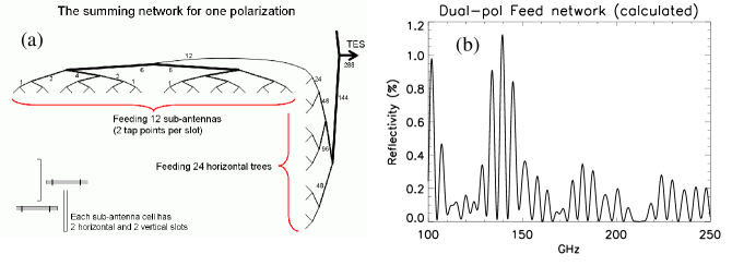
We use a combination of SuperMix library[14] and SONNET simulation software to optimize the design of the summing network. At the sub-antennas, the microstrip has to match the real part of the slot impedance. The signals from sub-antennas with the same polarization are combined by a network of T-junctions, as shown in Figure 3(a). These matched T-branches decrease the impedance downstream, since . Tapered impedance transformers between T-junctions have to be used to maintain the downstream microstrips at manageable widths.
For a given application, the geometry of the sub-antenna cell (the slot length, width, gap, etc.) is determined by the desired operating impedance, while the array size is fixed by the wavelength and the desired FHWM. These constraints prevent the use of simple binary trees and further complicates the design of the summing network. For and FWHM , the array format is usually in the -cell range. Finally, the full summing network, made of multi-level tapered microstrips and branches, has to be routed through the gaps between the slot sub-antennas and connected to the TES (Figure 2a).
The seemingly daunting design challenge is greatly simplified by the following observation. We assign a weight factor to each microstrip branch, defined to be the number of sub-antennas from which the signal on the microstrip originated, as shown in Figure 3(a). For an impedance-matched summing network, the product of the local impedance and the weight factor should only be a function of the electrical distance to the slots, and independent of the particular location of that microstrip branch. For a fixed total length and fixed end impedances, this reduces to a one-dimensional calculus of variation problem for . The well-known solution to this problem is the Klopfenstein taper [15]. For simplicity we adopt an exponential taper , and use piecewise linear microstrip transformer sections as an approximation. The reflectivity can be calculated by[15] . For our taper design the reflected power is less than 1% over a wide frequency range, see Figure 3(b). Since can be defined everywhere on the network, once a good design for is found, the local impedance on an arbitrary point on the network can be obtained by . The summing network is then laid out with the LEdit software. Following these procedures, we have corrected a design error in the feed network of a first generation antenna that has caused excessive reflections [5].
2.3 The microstrip in-line filters
In the planned CMB applications, the combination of absorptive, quasi-optical, and microstrip filters are used to reject out-of-band radiation. In particular, the microstrip filters define both the upper and lower frequency cutoff of the science bands. The choice of the frequency bands in a CMB experiment is a trade-off between sensitivity, foreground information, detector readout counts, and optical performance, all under the constraint of a fixed focal plane area. Although 30% bandwidth is possible with our antenna design, we have chosen a nominal 25% fractional bandwidth for the bandpass filters, mainly because of the bandwidth limit of the half-wave plate in the optical train.
We have developed a lumped-element 3rd order bandpass Chebyshev filter, consisting of CPW inductors and stub capacitors. This compact filter design does not include any “vias” (direct electrical contacts to the ground plane), and is fully compatible with photolithographic processes. Because of their non-resonant nature, these filters do not have fundamental harmonic leaks. The bandgap frequency (690 GHz) of niobium microstrips provides a natural high frequency cutoff for CMB experiments. In the past 3 years we have fabricated and tested more than a dozen such filters, with operating frequencies ranging between 90 and 250 GHz. Every tested filter so far shows sharp low and high frequency cutoff, high in-band transmission, and very low high frequency leaks. The challenge has been to repeatedly and reliably produce filters with the correct center frequency to one- or two- percent level, and to control the detailed shape of the transmittance. The measured spectra of the first generation devices showed higher central frequencies then the calculated values [5]. The cause was traced to the fabrication uncertainty of the dielectric thickness. This issue has been resolved, by using a 6-inch SiO2 target and better monitoring of the dielectric thickness during and after deposition. See §3.2 for the measured performance of the antennas and filters.
2.4 The TES bolometers
After the bandpass filter, the signal collected by the antenna is transmitted through the Nb microstrip, and readout by a microstrip-coupled, thermally isolated bolometer on a micro-machined silicon nitride (SiN) island. The microstrip enters the thermally isolated patch via a suspended SiN leg, and terminates in a meandering resistive microstrip (see Fig.1e). A TES film deposited on the isolated region, and readout via superconducting Nb leads, detects the heat from dissipation of electromagnetic energy in the resistor. The bolometer operates in the standard voltage bias configuration, which provides strong electrothermal feedback [16]. The principal benefits of this operating mode are linearity and rapid speed of response.
The termination resistor is made of a meander of gold open-ended microstrip. The un-absorbed EM wave is reflected at the end of the microstrip, as a result the effective length of the resistive microstrip is twice the physical length (2.2 mm). Since the characteristic impedance is largely determined by the geometry, the impedances of the superconducting and resistive microstrips are well-matched. The termination efficiency is calculated to be at 100 GHz. The advantages of this design are wide bandwidth and immunity to variations in the thickness and the resistivity of the lossy film. The same meandering microstrip can be used to terminate 30 GHz radiation with an efficiency of . A 3 mm long microstrip will absorb up to of the incoming power[5]. Another significant advantage of microstrip-coupled bolometer geometry is that the thermalization time constant is much shorter than the external (bolometer) time constant, providing excellent thermal efficiency.
The TES for the sub-orbital CMB experiments will be based on elemental titanium (Ti). It is known that the of Ti films is close to the bulk value and is fairly immune to thickness variations. To facilitate laboratory testing under high optical loading conditions, we developed a dual- TES (0.46 K and 1.2 K) made from Ti and Al films (Figure 1e). We carry out dark electrical and thermal tests of a prototype SPIDER[17] bolometer in a dilution refrigerator using a SQUID sensor (not multiplexed). We find that when biased at the Ti transition the TES exhibits white noise between 0.1 and 10 Hz, with an electrical NEP of . The natural time constant is around 20 ms, and reduces to 1 ms with electrothermal feedback [18]. The uniformity of the array parameters measured with a time-domain SQUID multiplexing system is reported in §3.4.
3 Array Fabrication and Performance
3.1 Fabrication
The antenna-coupled TES arrays are fabricated in the Microdevices Laboratory at JPL. The fabrication is accomplished using an assortment of lithography, deposition, and etching technologies. The process is quite challenging and many technical hurdles were overcome to make the process reliable. The early problems we have encountered include TES wiring shorts by the Nb residue, pinholes in the dielectric layer, microstrips peeling off under stress, and poor metal-dielectric adhesion due to HCl contamination. In the past few months we have reached the point where arrays with good yields can be reliably produced. The current process requires no wet etches, and can be carried out by patterning only the front side of the wafer.
| Material | Deposition | Patterning |
|---|---|---|
| Al | E-beam evap. | Lift-off |
| Ti | DC sputtering | ICP, Freon-12 |
| SiO2 | RF sputtering | ICP, CHF3/O2 |
| Nb | Magnetron sputtering | ICP, Cl3/BCl3 |
| Au | E-beam evap. | Lift-off |
| SiN | Grown on Si | ICP, CHF3/O2 |
| Si | NA | STS DRIE, XeF2 |
Since 2006, all lithography is performed with a Canon FPA 3000, deep ultra-violet, stepper mask aligner, allowing us to step and repeat many patterns on a 4-inch wafer. We found it necessary to use 6-inch Ti and SiO2 targets in order to achieve adequate thickness uniformity.
We start with silicon wafers that have a 1 thick layer of silicon nitride grown on the surface. The initial step is creating the Al-Ti dual- TES. After the Ti etch, we immediately dip the wafers in water to wash away any HCl that may have formed from Cl residue and moisture in the air. We find it necessary to introduce SiO2 passivation layers after the creation of the Dual-Tc TES structures, and between the Al and Ti depositions. The electrical connection between the two TESs and with the Nb wiring layer is made with etched windows on the passivation SiO2 layers.
The Nb ground plane is deposited by magnetron sputtering. Slots in the ground plane are patterned and ICP etched, then the wafers are again dipped in water. We then deposit the inter-layer dielectric (ILD) layer which separates the ground plane from a top Nb layer. The ILD is 285nm of SiO2 and is deposited by biased RF sputtering. The biasing is necessary to insure nice, smooth contours at step edges. The thickness of this layer is vital to ensuring the microstrips and filters perform as desired.
The uniformity results reported in §3.4 came from an early engineering grade wafer where a large fraction of the TESs are shorted by pinholes in the ILD. In order to solve this problem we create the ILD layer in two depositions. After the first deposition, the sample is removed, polished, ultrasounded and O2 plasma cleaned. The polishing dislodges any debris that may be loosely bound to the SiO2, opening up holes. The second SiO2 deposition fills in these holes. After the ILD has been deposited it is patterned and etched to create vias for connecting the TES’s to the top Nb layer. The top layer Nb is deposited, patterned, and etched with the same system, chamber, and parameters as the Nb ground plane layer. The top Nb layer contains the summing networks, TES DC wiring, and filters. The next step is creating the termination resistor (Au meander), which completes the electrical aspects of the TES array.
The final step is defining the thermally isolated membranes, perhaps the most challenging part of the fabrication process. The membranes are 150300 rectangles and are suspended and isolated by four, 3- wide legs, and two, 9- wide legs. The DC wiring and microstrip lines rest on the wider legs. The first step in defining the membranes is to etch the SiN in unwanted areas. The patterning for this is done with a 4 -thick photoresist. This etch exposes bare silicon in regions except those where the membrane and legs will be. After the SiN etch, a very thick ( 10 ) photoresist is patterned to define the membrane, and membrane legs. A thick resist is necessary because the exposed bare silicon is etched with an STS deep trench etcher, which cuts completely through the 500 thick wafer in 3 hours. The resist is not removed after the deep trench etching and is still thick enough to be used in the final step, a XeF2 gas etch which undercuts the silicon underneath the membrane and legs to thermally isolate the bolometers. Table 1 summarizes the fabrication methods for various layers.
3.2 Optical testing and results
At the time of writing the full receiver focal plane is still under construction and is not ready for array-level optical testing. We obtained optical data from individual detectors diced from an array. The detectors are tested in an optical testbed equipped with a closed-cycle 3He refrigerator. This is the same testbed we used to make the measurements reported in the previous SPIE paper [5]. There are however some modifications to the system. First of all, we have reconfigured the optical train to eliminate metal mesh filters at oblique angles, which may have contributed to the cross polarization signal seen earlier. In the current setup, we use thick (1.5 cm), PTFE filters [9] at 77K and 4K for thermal filtering. These filters are mounted face-on, and anti-reflection coated to minimize polarization artifacts. For some of the optical tests, we use an additional 2mm-thick carbon-loaded PTFE sheet to reduce in-band millimeter wave loading on the detectors. A quartz plate is glued (GE varnish) onto the silicon entry surface as the anti-reflection coating. In these tests the detectors are mounted in a copper box with no backshorts: the summing tree side of the detector is facing a piece of eccorsorb absorber.
The detectors are mounted in a superconducting niobium shield (with a 4.4-cm opening) during the measurements to guard the TES and the SQUID read-out against magnetic interference. For Al-Ti dual TES, the bolometers are biased at the Al transition. Some earlier devices have Mo-Au bi-layer films with 0.7K.
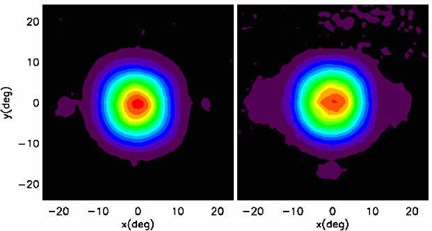
The beam pattern (angular response) of the antenna-coupled TES is measured with an optically modulated thermal source on a moving X-Y stage. Figure 4 show the measured co-polar radiation patterns for a detector pair. The beams are symmetrical, and well-matched (to level). Four minor sidelobes are visible, as predicted by physical optics models. In a refractive receiver (such as BICEP-2 and SPIDER), the sidelobes are terminated at the cold Lyot stop. The illumination of the pupil, and consequently the beam on the sky, is then determined by the mainlobes of the antenna radiation pattern. The FWHMx, FWHMy for the beams in Figure 4 are and , respectively. The center frequency for this earlier detector is 165 GHz. After scaled to the nominal frequency of 145 GHz, the FWHM should be around . Note that the dipole components of the differenced beam correspond to phase errors at the feed level and are not measurable with a thermal source. In the planned experiments, half-wave plates will be incorporated in the optics to reduce systematics associated with beam mismatch.
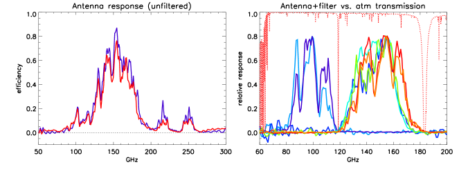
The end-to-end spectra of the devices are measured with a Fourier transform spectrometer (FTS). The normalized spectra for a pair of unfiltered dual- polarization antennas are plotted in the left panel (Figure 5a). We assume single-moded throughputs (), and correct for the effects of a Mylar beam-splitter when plotting the spectra. The observed center frequency agrees well with the design values (145GHz). The bandwidth is sufficient, but less than the predicted 39%, perhaps as a result of optical interference in the testbed, and to some degree, imperfect fabrication. The features at high frequency are caused by surface wave modes in the silicon wafer [13]. The FTS spectra in Figure 5(a) are normalized by measurements in a separate experiment, where the detectors are illuminated with a known optical power from a warm blackbody source (4.2K - 15K) [5]. Even without a backshort, the end-to-end optical efficiency is over 70% at the peak, higher than most micromesh semiconductor bolometers [8, 9, 10].
Figure 5(b) shows several representative spectra of the full antennafilter devices. The plotted spectra are not absolutely normalized, but the optical efficiency for a selected subset of the detectors are confirmed to be high as well. The design center frequencies are 96 GHz and 145 GHz, corresponding to two important atmospheric windows at mm-wavelengths. Also plotted is the atmospheric transparency at ballooning altitudes. The filter bands are within a few percent of the design values and are well-matched to the atmospheric windows. There is evidence for optical interference in the testbed and fabrication defects, which might have caused the observed structures and variations in the transmittance curves. We believe the shifts in the center frequencies between different fabrication runs are entirely due to variations in the dielectric thickness (SiO2).
We used a free-standing wire grid polarizer111MicroTech G-40L. to quantify the cross-polar response, also known as the polarization leakage. According to the manufacturer, the polarization leakage of the wire grid is between for the frequency range of GHz . Therefore the measured peak cross-polar response, 1% to 3% is entirely due to the devices. This level of polarization leakage is comparable or better than the semiconductor-based feedhorn coupled polarization sensitive detectors used in BICEP, QUAD, and Planck. The angular distribution of the cross-polar response has not been measured.
The small cross-polar response, which varies between detectors, is most likely caused by unseen shorts, breaks, or other defects in the summing networks. This should be improved with better controlled fabrication procedures. As an example, the optically measured detectors are fabricated with a single ILD deposition (§3.1) and might contain pinholes. A two-step ILD process has become part of the standard procedure and should improve the reliability of the summing networks.
3.3 Dielectric/microstrip testing
The performances of the summing networks and the filters depend on correct modeling of the dielectric and microstrip behavior. The most important parameters are the dielectric constant and loss tangent of the ILD (SiO2), and the kinetic inductance of the Nb microstrips.
We developed a series of TES devices aiming at measuring these properties. In the first test device, 2 TES are coupled to a common single polarization slot antenna through a 3-dB power divider. One of the outputs of the power divider is connected to a reference TES (TES-1) through an impedance-matching microstrip. The other output is connected to TES-2 through a microstrip that has a wider section, see Figure 6a. The reflection from the impedance discontinuities generates interference. We use the SONNET software to calculate the expected signal at TES-1 and TES-2, and compare the results with the FTS measurements. The reflected wave can travel to TES-1, but the ratio of the signals in the 2 TESs exhibits prominent interference fringes. The frequency spacing of the fringes is a direct measurement of the phase velocity of the wide microstrip section, or equivalently, the imaginary part of the propagation constant (Figure 6b). From the fringes we find that and fall along the line , where is measured in per square. This result is quite insensitive to the ILD thickness of test device, since , and thickness variation tends to cancel since it drives and in the opposite directions. The transmittance of the microstrip filter is used to break the degeneracy between and , because in our filter design the inductance is dominated by geometrical inductance. Comparing SONNET simulations of the filters and the FTS measurements, we determined that .
A second test device consists of a pair of notch filters (Figure 6 c). Convincing notch frequencies are observed at 133 GHz and 167 GHz, which agree to within 5% of the SONNET simulations. However, through its dependence on , this measurement is sensitive to the thickness variations of the ILD in the test device. We have decided to rely on the phase velocity measurements and the band-pass filters to derive the parameters, and use the notch filters only as a consistency check.
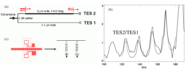
The third test device was developed to measure the loss tangent of the dielectric material SiO2. The design is similar to the test device for the phase-velocity measurements, with the wide microstrip section in Figure 6(a) replaced by a very long, meandering Nb microstrip (3.1 11.4 cm). The device is illuminated with a chopped thermal source, and the signals at TES2 and TES1 are compared. After correcting for the responsivity we obtain an attenuation constant cm-1, corresponding to a dielectric loss tangent of at 145 GHz. This translates into a negligible loss contribution from the feed network in an antenna-coupled bolometer, which typically has 2-3 cm of microstrip lines from the slots to the TES. This low loss is consistent with the measured high optical efficiency.
It is worth noting that the loss measurements are carried out at sub-Kelvin temperatures, and the modulated signal is small. This is important because the dielectric loss is a strong function of temperature and excitation power [19]. The loss tangent quoted above is representative of what we expect in a CMB experiment.
3.4 Array uniformity
We have conducted dark measurements of an antenna-couple TES array with the full SQUID multiplexing system. The TESs of the array are read out by 4 NIST SQUID multiplexer (MUX) chips, each MUX chip reading out 32 TESs. Additionally, 4 NIST “Nyquist” (NYQ) chips are used in conjunction with the MUX chips to roll off high frequency noise. The shunt(bias) resistors are fabricated on the NYQ chips. We employ time-domain multiplexing[6] to read out the array in a 4 column by 32 row format, using the Multi-Channel Electronics (MCE) system developed at University of British Columbia. The columns are defined by the 4 sets of NYQ/MUX chips, while the rows are defined by the 32 first stage SQUIDS each inductively coupled to a TES. The 4 columns (MUX chips) share the same sets of row addressing (RA) lines. And we have one pair of bias lines per NYQ chip, whereby the 32 TESs of a given column are biased in series.
The 128-element array tile is mounted on a gold-plated copper stage, cooled to a base temperature of 260mK by a 3-stage (3He/4He/3He) Helium refrigerator. It is held to the stage by beryllium-copper spring clips fixed near the corners of the array, with a thin layer of plastic shim between. Also attached to the 260mK stage is a multi-layer printed circuit board, used as the attachment point for the NYQ and MUX chips. The PCB also provides routing for the control wiring for the NYQ/MUX chips and the signal lines that connect them to the TES array. The TES signal lines are superconducting; formed on the top layer of the PCB by aluminum sputtered onto copper lines. The NYQ/MUX chip control wiring is distributed within the multiple layers of the PCB, such that the signal and return lines of the row addressing lines overlap to reduce pickup loops. Connection between control and signal wiring and the array and NYQ/MUX chips is made using 0.001” aluminum wirebonds. The NYQ/MUX chips are mounted on the PCB using an intermediary alumina carrier, which has been selected due to the similar coefficients of thermal expansion of alumina and silicon. The carriers are first attached to copper pads on the PCB using indium solder. The NYQ and MUX chips are expoxied to the carriers side-by-side. The array mounting/wiring scheme developed for this single array testbed remains unchanged in the 4-tile focal plane of the planned CMB experiments. Figure 1(b) shows the mounting of 4 arrays and NYQ/MUX chips, the PCB with aluminized traces, and the Al wire bonds.
The array tested is a SPIDER engineering grade array, with a designed TES transition of 450mK, and a thermal conductance of pW/K. Shortly after the array was mounted we discovered that many of the TESs suffer from the ILD pinholes and are shorted to the ground plane and the chassis. In addition, there is a first-stage SQUID failure and some wire bonding issues. The total number of operational TESs is 60 out of 128. The yield will greatly increase in the future, since we have identified and improved the ILD pinhole problem and the SQUID/wire bonding quality should improve with more experience. The measured mean and RMS of the TES parameters are summarized in Table 2.
| Parameter | Mean | RMS | Target |
|---|---|---|---|
| (mK) | 466 | 3.9 | 450 |
| Rn (m) | 61.9 | 10.8 | 60 |
| G450 (pW/K) | 13.6 | 1.67 | 19 |
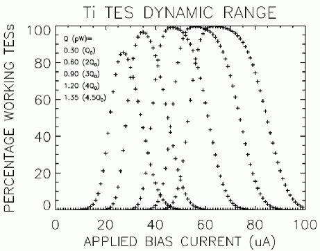
Given these mean values and their spreads, a determination can be made of the number of functional TESs a system will have under a range of optical loading, . We used a Monte Carlo simulation to calculate the effect of the mean and spread of the values detailed above in the power balance equation for a TES.
| (1) |
where is the optical power, , are the bath temperature and the transition temperature, and the bias voltage. defines the temperature dependent thermal conductance of the bolometer. The equation was solved for the TES operating resistance, and a TES was considered operational if this value was between 0.3 and 0.95 times the normal resistance for a given applied TES bias. The fraction of operational detectors was calculated for a range of applied TES biases, which yields the optimal bias point for a given . The was then stepped through 0.3, 0.6, 0.9, 1.2 and 1.35 pW, and the family of curves was plotted in Figure 7. The figure depicts the dynamic range of the TES array given varying optical loading conditions. The optical loading can increase from the nominal value of 0.3pW to 1.35pW with a loss of roughly 15% of the TESs after properly adjusting the bias.
4 Future Plans
So far we have successfully demonstrated 145 GHz and 96 GHz devices, and have obtained a design for 225 GHz. We will continue to extend the frequency coverage of this technology to both high and low frequencies, and to improve fabrication and uniformity of the TES arrays. Other direction of detector development may be a detailed study of the dielectric/microstrip properties. Such information can be used to improve the design of the summing network and on chip microstrip hybrids that can be used for simultaneous detection. The summing networks can be tapered to lower the sidelobes, or phase lagged to allow for non-telecentric optical systems.
These detectors will first be used in the upgrade of the BICEP experiment [9], “BICEP-2”, and SPIDER, a balloon-borne experiment [17]. BICEP-2 and SPIDER share common design concepts, including large throughput cold refractive telescopes that produce extremely low cross-polarization, instrument polarization, instrument loading, and beam ellipticity. The 30 cm compact optics enables detailed pre-flight/deployment characterizations, and provides an angular resolution of suitable for primordial B-mode polarization.
Despite these similarities, the two experiments are based on very different observing strategies. SPIDER is targeting very large angular scale CMB polarization, including the re-ionization bump at . It will survey 50% of the sky. To facilitate Galactic foreground removal on large angular scales, SPIDER payload consists of 6 telescopes, covering a wide frequency range (80-275 GHz) with 2000 antenna-coupled TES bolometers. On the other hand, BICEP-2 and its successor SPUD will be observing from South Pole mainly through the 2mm and 3mm atmospheric windows. With the long integration time available from the ground, it will go extremely deep on 1-2% of the sky that has minimum astronomical foregrounds.
Both experiments will be important scientific pathfinders for CMBPol, a comprehensive NASA satellite to study the CMB polarization [1]. In addition, many technical aspects discussed in this paper will be thoroughly tested. State-of-the-art photolithography can now reliably produce silicon nitride legs with extremely high aspect ratio. The NEP required by a space-borne CMB mission is now routinely achieved in the laboratory with appropriate time constant, using TES materials that have lower such as Mo/Cu or Mo-Au bi-layers. To produce bi-layers with highly controlled poses some fabrication challenge, but is definitely possible. The current SQUID MUX can multiplex up to 32 channels [6]. In the future, the microwave frequency domain SQUID MUX [20] with reflectometer readout might be able to multiplex hundreds or even thousands of detectors, with electronics at a much lower cost. We believe the antenna-coupled TES detector technology is a strong candidate for CMBPol.
Acknowledgements.
The authors acknowledge support from the JPL Research and Technology Development program, a NASA/APRA grant “Antenna-Coupled TES Bolometer Array for CMB Polarimetry” to J. Bock, and the Gordon and Betty Moore foundation.References
- [1] J. Bock, S. Church, M. Devlin, G. Hinshaw, A. Lange, A. Lee, L. Page, B. Partridge, J. Ruhl, M. Tegmark, P. Timbie, R. Weiss, B. Winstein, and M. Zaldarriaga, “Task Force on Cosmic Microwave Background Research,” astro-ph 0604101, Apr. 2006.
- [2] W. C. Jones et al., “A Polarization Sensitive Bolometric Receiver for Observations of the Cosmic Microwave Background,” in Millimeter and Submillimeter Detectors for Astronomy. Proceedings of the SPIE, Volume 4855, T. G. Phillips and J. Zmuidzinas, eds., pp. 227–238, Feb. 2003.
- [3] M. J. Myers et al., “An antenna-coupled bolometer with an integrated microstrip bandpass filter,” Applied Physics Letters 86, pp. 4103–+, Mar. 2005.
- [4] D. Chuss et al., “The Primordial Anisotropy Polarization Pathfinder Array (PAPPA): Instrument Overview And Status,” in Proceedings of the SPIE, 2006.
- [5] C. L. Kuo et al., “Antenna-coupled TES bolometers for CMB polarimetry,” in Millimeter and Submillimeter Detectors and Instrumentation for Astronomy III. Edited by Zmuidzinas, Jonas; Holland, Wayne S.; Withington, Stafford; Duncan, William D.. Proceedings of the SPIE, Volume 6275, pp. 62751M (2006)., Presented at the Society of Photo-Optical Instrumentation Engineers (SPIE) Conference 6275, astro-ph/0606366, July 2006.
- [6] P. de Korte et al., “Time-division superconducting quantum interference device multiplexer for transition-edge sensors,” Review of Scientific Instruments 74, pp. 3807–3815, Aug. 2003.
- [7] T. M. Lanting et al., “Frequency-domain multiplexed readout of transition-edge sensor arrays with a superconducting quantum interference device,” Applied Physics Letters 86, pp. 2511–+, Mar. 2005.
- [8] T. E. Montroy et al., “A Measurement of the CMB EE Spectrum from the 2003 Flight of BOOMERANG,” Astrophysical Journal 647, pp. 813–822, Aug. 2006.
- [9] K. W. Yoon et al., “The Robinson Gravitational Wave Background Telescope (BICEP): a bolometric large angular scale CMB polarimeter,” in Millimeter and Submillimeter Detectors and Instrumentation for Astronomy III. Edited by Zmuidzinas, Jonas; Holland, Wayne S.; Withington, Stafford; Duncan, William D.. Proceedings of the SPIE, Volume 6275, pp. 62751K (2006)., Presented at the Society of Photo-Optical Instrumentation Engineers (SPIE) Conference 6275, astro-ph 0606278, July 2006.
- [10] QUaD collaboration: J. Hinderks et al., “QUaD: A High-Resolution Cosmic Microwave Background Polarimeter,” astro-ph 08051990, May 2008.
- [11] M. J. Griffin, J. J. Bock, and W. K. Gear, “Relative performance of filled and feedhorn-coupled focal-plane architectures,” Applied Optics 41, pp. 6543–6554, Nov. 2002.
- [12] W. Hu, M. M. Hedman, and M. Zaldarriaga, “Benchmark parameters for CMB polarization experiments,” Physical Review D 67, pp. 043004–+, Feb. 2003.
- [13] P. Day et al. In preparation , 2008.
- [14] J. Ward, F. Rice, G. Chattopadhyay, and J. Zmuidzinas, “SuperMix: A Flexible Software Library for High-Frequency Circuit Simulation, Including SIS Mixers and Superconducting Elements,” in Proceedings of Tenth International Symposium on Space Terahertz Technology, pp. 268–281, 1999.
- [15] D. M. Pozar, Microwave Engineering, 3rd Ed., John Wiley & Sons, 2005.
- [16] K. D. Irwin, “An application of electrothermal feedback for high resolution cryogenic particle detection,” Applied Physics Letters 66, pp. 1998–2000, Apr. 1995.
- [17] T. E. Montroy et al., “SPIDER: a new balloon-borne experiment to measure CMB polarization on large angular scales,” in Ground-based and Airborne Telescopes. Edited by Stepp, Larry M.. Proceedings of the SPIE, Volume 6267, pp. 62670R (2006)., Presented at the Society of Photo-Optical Instrumentation Engineers (SPIE) Conference 6267, July 2006.
- [18] J. A. Bonetti et al., “Electrical and Thermal Characterization of Membrane-Isolated, Antenna-Coupled, TES Bolometers for the SPIDER Experiment,” Journal of Low Temperature Physics 151, pp. 138–143, Apr. 2008.
- [19] M. von Schickfus and S. Hunklinger, “Saturation of the dielectric absorption of vitreous silica at low temperatures,” Physics Letters A 64, pp. 144–146, Nov. 1977.
- [20] K. D. Irwin and K. W. Lehnert, “Microwave SQUID multiplexer,” Applied Physics Letters 85, pp. 2107–+, Sept. 2004.