Probing the momentum relaxation time of charge carriers
in ultrathin semiconductor layers
Abstract
We report on a terahertz time-domain technique for measuring the momentum relaxation time of charge carriers in ultrathin semiconductor layers. The phase sensitive modulation technique directly provides the relaxation time. Time-resolved THz experiments were performed on n-doped GaAs and show precise agreement with data obtained by electrical characterization. The technique is well suited for studying novel materials where parameters such as the charge carriers’ effective mass or the carrier density are not known a priori.
pacs:
87.50.U-, 78.47.J-, 73.50.-h, 78.66.Db, 78.20.-eI Introduction
Terahertz (THz) time-domain spectroscopy (TDS) has developed towards an alternative technique for characterizing electrical transport in condensed matter. Many studies on semiconductors demonstrate excellent agreement with the Drude model and characteristic properties such as the complex conductivity have been deduced van Exter and Grischkowsky (1990a, b). One of the most fundamental quantities which describe charge transport is the Drude momentum relaxation time . Deducing from optical data demands knowledge of further parameters, such as of the carriers’ density , the effective mass , the background permittivity , and the thickness of the sample van Exter and Grischkowsky (1990a); Schall and Jepsen (2000); Mycomment01 (2000). The latter can be deduced in time-resolved THz experiments when the optical thickness exceeds the wavelength of the radiation Duvillaret et al. (1999); Dorney et al. (2001). However, the progress in material science provides many novel materials, which are extremely thin and have unknown charge carrier densities and effective masses. Recently, terahertz spectroscopy as well as far-infrared and microwave techniques are used for characterizing modern materials Hoofman et al. (1998); Fischer et al. (2006); Parkinson et al. (2007). But these approaches require precise knowledge of material parameters or use fitting procedures.
In this work, we present an optical method for probing the Drude relaxation time without using any further parameters. In our technique we modulate the optical properties of the sample and record the differential response signal at THz frequencies. We will show that the phase of this signal directly provides the relaxation time. It is worth pointing out, that our method is not restricted to the THz band. The method can be adapted to any spectroscopic technique, which provides the optical phase of transmitted or reflected radiation.
Small modulations of the sample’s optical properties can be achieved most conveniently by electromodulation techniques similar to the method described by Allen et al. Allen Jr. et al. (1975). The fact that the modulation of the charge carrier density resembles the operation of a field-effect transistor illustrates the application potential of the technique. Currently, numerous novel materials such as nano-structures or organic semiconductors have been developed for similar devices. Many of these materials, however, are inhomogeneous, include a high density of traps and grain boundaries, or have a broadened density of electronic states. Dispersive transport and hopping dominate electrical properties and mask the fundamental carrier dynamics on microscopic scales Scher and Montroll (1975); Pollak (1977). In such cases THz modulation spectroscopy may provide an unambiguous insight into the fundamental carrier relaxation dynamics.
II Method
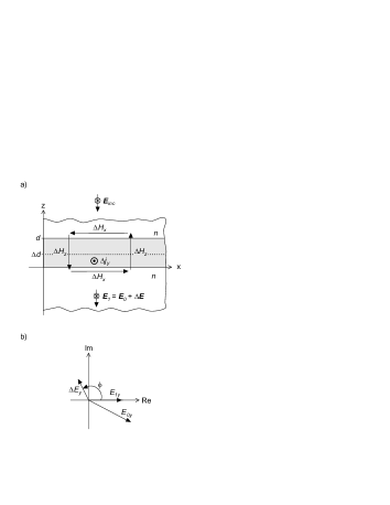
The concept of our method is illustrated in Fig. 1a). We study a thin sheet of a semiconductor, which has the thickness and contains mobile carriers. Within the small fraction the charge carrier density can be modulated, e.g. the density can be reduced to zero. A fraction of an incident THz electric field is transmitted through the doped layer, and generates a current density j which is proportional to the complex conductivity . In the following, it is convenient to discuss differential quantities such as the differential field where and are the transmitted electric fields in the case of an interaction across the entire layer and in the case the layer thickness is reduced by , respectively. The differential current density can be described by a change of the thickness
| (1) |
where we assumed the electric field to be virtually constant across the layer, which is a valid approximation for optically thin films. In order to deduce the impact of on the reflection and transmission of radiation, we consider that causes a differential magnetic field , which can be calculated by Ampere’s law:
| (2) |
In layers which are thin compared with the wavelength , the x-components of dominate the above equation whereas the z-components can be neglected. We also consider that is smaller than the skin depth. In consequence, the modulated current density does not change significantly across the depleted layer. The magnetic field causes a differential electrical field given by , where is the impedance of vacuum and is the refractive index of the surrounding medium. Using as reference provides:
| (3) |
In the Drude model the complex conductivity is
| (4) |
where is the carrier density and is the carrier’s effective mass Drude (1900); Ashcroft and Mermin (1976). Relating the imaginary part of to the real part yields the optical phase of the signal:
| (5) |
Thus, the momentum relaxation time can be directly deduced from without the use of further parameters. Figure 1b) displays the fields in the complex plane.
Alternatively, the amplitude or intensity of the signal can be analyzed in case that Dressel and Gruner (2002). In the Hagen-Rubens range (), however, the spectra become structureless because the amplitude is proportional to . In contrast, the phase is proportional to , which illustrates the strength of our technique when characterizing materials in which ultrafast scattering occurs.
III Experimental
We tested the method on a GaAs structure grown by molecular beam epitaxy (MBE). It comprises an n-doped layer grown on a semi-insulating GaAs substrate. The layer is doped at cm-3 and has a thickness of 2 m. For electronic control we fabricated a Schottky contact on top of the structure by depositing a 10 nm thick film of Cr. The second terminal is an Ohmic AuGe contact. The doped layer in the GaAs can be partially depleted from electrons by the application of a negative bias to the Schottky contact Sze (1985). In our experiments the changes of the layer thicknesses are of the order of 100 nm. This is much smaller than the skin depth of the electron gas, which is about 20 m at THz frequencies. Thus, the assumptions made in section II are justified. They can be applied to many other devices where conductive sheets are modulated, as for instance, in field-effect transistors.

In our experiments we apply time-resolved THz transmission spectroscopy. The sample is mounted in a cryostat, which allows for low-temperature measurements. A titanium-sapphire laser delivers pulses of 80 fs duration at 780 nm center wavelength and at a repetition rate of 80 MHz. About 700 mW of the laser power is used for the photoexcitation of an interdigitated THz emitter Dreyhaupt et al. (2005); Acuna et al. (2008). Parabolic mirror optics with focus the THz radiation onto the GaAs structure. The transmitted radiation is time-resolved by standard electro-optic sampling in a [110] ZnTe crystal of 1 mm thickness Wu and Zhang (1996). The setup has a bandwidth of 2.8 THz and the signal to noise ratio is about Hz1/2. We measured the field strength of the THz pulses using the procedure described in Ref. Planken et al. (2001) and deduced a peak field of 70 V/cm. The upper curve in Fig. 2 shows a THz pulse transmitted through the GaAs structure. The lower curve displays the differential signal, which we obtained by modulating the structure with a bias of -5 V. This corresponds to a change of the depletion width of about 400 nm.
IV Results and discussion
In order to prove the concept of our technique we measured the differential transmission through the GaAs structure at room temperature. The electron gas was modulated by switching the bias to the Schottky contact between 0 V and -1 V. This corresponds to a modulated layer thickness of 120 nm or to a modulated sheet density of cm-2. We recorded the THz signals and Mycomment02 (2000). After Fourier transform of the differential THz signal , the optical phase was obtained as described above. The data depicted in Fig. 3 show the expected dependence of the phase on the frequency. Using a relaxation time of 198 2 fs provides an excellent agreement with eq. (5). Additionally, the data indicate a phase of for zero frequency, which is characteristic of the Drude model.


In section II we assumed that only the lateral components of contribute to Ampere’s law whereas the perpendicular components can be neglected. We also assumed that the exciting THz field is virtually constant across the modulated layer. We validate these assumptions by measuring the THz signals in dependence on the modulation depth by increasing the modulation voltage . The results are summarized in Fig. 4. The measured phase shows no dependence on , which proves the validity of the assumptions. In contrast, the amplitude follows a square root dependence as expected for the increase of the depletion width with voltage Sze (1985). The calculation of the amplitude shows deviations for higher voltages. We attribute these differences to imperfections of the Schottky contact and to inhomogeneities of the doping profile. This illustrates the difficulties that arise in deducing transport properties from amplitude data and highlights the reliability of phase measurements.

In the case of our well-defined MBE grown structure, parameters such as the doping density and effective carrier mass are well known. Thus in this particular case, the momentum relaxation time can be extracted from four-point measurements Smits (1958). Figure 5 shows temperature resolved data. Electrical and phase measurement differ by about 3%, which illustrates that our technique provides precise data. At low temperatures, however, freeze-out of the donors may lead to a reduced electrical conductivity, which explains the differences at about 100 K. We emphasize that our approach is not advantageous in the case of homogeneous semiconductors with well known properties. In this case electrical characterization certainly is less elaborate. Besides the fact that many modern materials exhibit unknown charge carrier densities and effective masses, most of them are inhomogeneous. In such systems grain boundaries may limit electrical transport and in consequence extremely low mobilities are observed by electrical characterization. Examples are polycrystalline semiconductors, percolated networks of carbon nanotubes, and many organic substances where hopping transport is the most limiting factor. Here, THz phase analysis may open up new opportunities for measuring the Drude momentum relaxation rate.
V Conclusions
We developed a technique for directly measuring the momentum relaxation time of charge carriers using the optical phase of a differential THz signal. The modulation of the structure under investigation provides a phase signal which is proportional to . In contrast to other spectroscopical approaches, our technique is advantageous particularly in the Hagen-Rubens range. Thus, we are confident that our technique will provide new insights into many modern materials where scattering occurs on ultrafast time scales and electronic properties are not directly accessible by electronic means.
Acknowledgments
This work is partially supported by the Deutsche Forschungsgemeinschaft (DFG) through the Nanosystems Initiative Munich (NIM), and by the Deutsche Forschungsgemeinschaft (DFG), contract Ke 516/1-1. The authors acknowledge technical support by A. Guggenmos and S. Niedermaier.
References
- van Exter and Grischkowsky (1990a) M. van Exter and D. Grischkowsky, Appl. Phys. Lett. 56, 1694 (1990a).
- van Exter and Grischkowsky (1990b) M. van Exter and D. Grischkowsky, Phys. Rev. B 41, 12140 (1990b).
- Schall and Jepsen (2000) M. Schall and P. Jepsen, Optics Letters 25, 13 (2000).
- Mycomment01 (2000) In fact, the THz response scales with the sample’s plasma frequency given by carrier density effective mass and background permittivity.
- Duvillaret et al. (1999) L. Duvillaret, F. Garet, and J.-L. Coutaz, Appl. Opt. 38, 409 (1999).
- Dorney et al. (2001) T. D. Dorney, R. G. Baraniuk, and D. M. Mittleman, J. Opt. Soc. Am. A 18, 1562 (2001).
- Hoofman et al. (1998) R. J. O. M. Hoofman, M. P. de Haas, L. D. A. Siebeles, and J. M. Warman, Nature 392, 54 (1998).
- Fischer et al. (2006) M. Fischer, M. Dressel, B. Gompf, A. K. Tripathi, and J. Pflaum, Appl. Phys. Lett. 89, 182103 (2006).
- Parkinson et al. (2007) P. Parkinson, J. Lloyd-Hughes, Q. Gao, H. H. Tan, C. Jagadish, M. B. Johnston, and L. M. Herz, Nano Lett. 7, 2162 (2007).
- Allen Jr. et al. (1975) S. J. Allen Jr., D. C. Tsui, and F. DeRosa, Phys. Rev. Lett. 35, 1359 (1975).
- Dressel and Gruner (2002) M. Dressel and G. Grüner, Electrodynamics of Solids - Optical Properties of Electrons in Matter (Cambridge University Press, 2002).
- Scher and Montroll (1975) H. Scher and E. W. Montroll, Phys. Rev. B 12, 2455 (1975).
- Pollak (1977) M. Pollak, Phil. Mag. 36, 1157 (1977).
- Drude (1900) P. Drude, Annalen der Physik 10, 566 (1900).
- Ashcroft and Mermin (1976) N. Ashcroft and N. Mermin, Solid State Physics (Harcourt, 1976).
- Sze (1985) S. Sze, Semiconductor Devices (John Wiley & Sons, 1985).
- Dreyhaupt et al. (2005) A. Dreyhaupt, S. Winnerl, T. Dekorsy, and M. Helm, Appl. Phys. Lett 86, 121114 (2005).
- Acuna et al. (2008) G. P. Acuna, F. F. Buersgens, C. Lang, M. Handloser, A. Guggenmos, and R. Kersting, Electr. Lett. 44, 3 (2008).
- Wu and Zhang (1996) Q. Wu and X.-C. Zhang, Appl. Phys. Lett. 68, 1604 (1996).
- Planken et al. (2001) P. C. M. Planken, H.-K. Nienhuys, H. J. Bakker, and T. Wenckebach, J. Opt. Soc. Am. B 18, 313 (2001).
- Mycomment02 (2000) To be more specific, and were measured after passage through the GaAs-wafer and the optical detection system. This does not affect differential quantities.
- Smits (1958) F. M. Smits, The Bell System Technical Journal 37, 711 (1958).