Smooth electron waveguides in graphene
Abstract
We present exact analytical solutions for the zero-energy modes of two-dimensional massless Dirac fermions fully confined within a smooth one-dimensional potential , which provides a good fit for potential profiles of existing top-gated graphene structures. We show that there is a threshold value of the characteristic potential strength for which the first mode appears, in striking contrast to the non-relativistic case. A simple relationship between the characteristic strength and the number of modes within the potential is found. An experimental setup is proposed for the observation of these modes. The proposed geometry could be utilized in future graphene-based devices with high on/off current ratios.
pacs:
73.21.-b, 03.65.Ge, 03.65.Pm, 81.05.UwI Introduction
Klein proposed that relativistic particles do not experience exponential damping within a barrier like their non-relativistic counterparts, and that as the barrier height tends towards infinity, the transmission coefficient approaches unity.Klein This inherent property of relativistic particles makes confinement non-trivial. Carriers within graphene behave as two-dimensional (2D) massless Dirac fermions, exhibiting relativistic behavior at sub-light speedDiracFermions ; CastroNetoReview owing to their linear dispersion, which leads to many optical analogies. Lens ; LevitovParabolic ; ZBZcombined ; Beenakker_PRL_102_2009 ; Chen_APL_94_2009 Klein tunneling through p-n junction structures in graphene has been studied both theoretically LevitovParabolic ; KleinCombined ; Cheianov_Falko_PRB(R)_74_2006 ; Peeters_PRB_74_2006 ; Chaplik_JETP_84_2006 ; Peeters_APL_90_2007 ; Fogler_PRL_100_2008 ; Fogler_PRB_77_2008 ; BeenakkerRMP08 ; ChineseShape and experimentally. Transport PN ; TopGateCombined ; Kim_PRL_99_2007 ; Savchenko_NanoLett_8_2008 ; Liu_APL_92_2008 ; GG_PRL_102_2009 ; Kim_NatPhys_5_2009 Quasi-bound states were considered in order to study resonant tunneling through various sharply terminated barriers. LevitovParabolic ; Peeters_PRB_74_2006 ; Chaplik_JETP_84_2006 ; Peeters_APL_90_2007 ; ChineseShape We propose to change the geometry of the problem in order to study the propagation of fully confined modes along a smooth electrostatic potential, much like photons moving along an optical fiber.
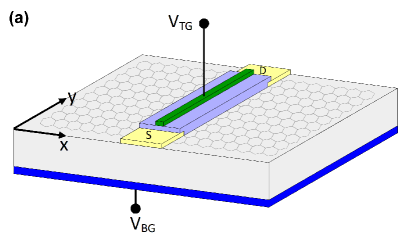
So far quasi-one-dimensional channels have been achieved within graphene nanoribbons, CastroNetoReview ; Nanoribbons ; RibbonTheoryCombined ; Efetov_PRL_98_2007 ; Peres_JPhysCondMat_21_2009 however, controlling their transport properties requires precise tailoring of edge termination,RibbonTheoryCombined currently unachievable. In this paper we claim that truly bound modes can be created within bulk graphene by top gated structures, Kim_PRL_99_2007 ; Savchenko_NanoLett_8_2008 ; Liu_APL_92_2008 ; GG_PRL_102_2009 ; Kim_NatPhys_5_2009 such as the one shown in Fig. 1(a). In an ideal graphene sheet at half-filling, the Fermi level is at the Dirac point and the density of states for a linear 2D dispersion vanishes. In realistic graphene devices the Fermi level can be set using the back gate. This is key to the realization of truly bound modes within a graphene waveguide, as zero-energy modes cannot escape into the bulk as there are no states to tunnel into. Moreover the electrostatic confinement isolates carriers from the sample edges, which are considered as a major source of intervalley scattering in clean graphene.SavchenkoSSC09
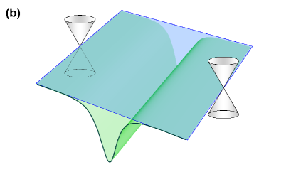
In this paper we obtain an exact analytical solution for bound modes within a smooth electrostatic potential in pristine graphene at half-filling, count the number of modes and calculate the conductance of the channel. The conductance carried by each of these modes is comparable to the minimal conductivity of a realistic disordered graphene system. DiracFermions ; Min. Con1 ; MinConTheoryCombined ; DasSarma_PNASUSA_104_2007 For the considered model potential we show that there is a threshold potential characteristic strength (the product of the potential strength with its width), for which bound modes appear. Whereas a symmetric quantum well always contains a bound mode for non-relativistic particles, we show that it is not the case for charge carriers in graphene.
II Fully confined modes in a model potential
The Hamiltonian of graphene for a two-component Dirac wavefunction in the presence of a one-dimensional potential is
| (1) |
where are the Pauli spin matrices, and are the momentum operators in the and directions respectively and m/s is the Fermi velocity in graphene. In what follows we will consider smooth confining potentials, which do not mix the two non-equivalent valleys. All our results herein can be easily reproduced for the other valley. When Eq. (1) is applied to a two-component Dirac wavefunction of the form:
where and are the wavefunctions associated with the and sublattices of graphene respectively and the free motion in the -direction is characterized by the wavevector measured with respect to the Dirac point, the following coupled first-order differential equations are obtained:
| (2) |
| (3) |
Here and energy is measured in units of .
For the treatment of confined modes within a symmetric electron waveguide, , it is convenient to consider symmetric and anti-symmetric modes. One can see from Eqs. (2-3) that and are neither even nor odd, so we transform to symmetrized functions:
The wavefunctions and satisfy the following system of coupled first-order differential equations:
| (4) |
| (5) |
For an ideal graphene sheet at half-filling the conductivity is expected to vanish due to the vanishing density of states. When the Fermi energy is at the Dirac point () there are no charge carriers within the system, so graphene is a perfect insulator. However all available experiments demonstrate non-vanishing minimal conductivity DiracFermions ; CastroNetoReview ; Min. Con1 of the order of which is thought to be due to disorder within the system CastroNetoReview ; MinConTheoryCombined ; DasSarma_PNASUSA_104_2007 ; PercolationNetwork or finite-size effects.SizeEffectCombined ; Beenakker_PRL_96_2006 In order to study confined states within and conductance along an electron waveguide it is necessary to use the back gate to fix the Fermi energy () at zero, as shown in Fig. 1(b). Note that Fig. 1(a) is just a schematic of the proposed experimental geometry and that side contacts may be needed to maintain the ‘bulk’ Fermi level at zero energy. The conductivity of the graphene sheet is a minimum and for a square sample the conductance is of the order of the conductance carried by a single mode within a waveguide. Thus the appearance of confined modes within the electron waveguide will drastically change the conductance of a graphene flake. Indeed each mode will contribute , taking into account valley and spin degeneracy. For device applications the sample should be designed in such a way that the contribution to the conductance from the confined modes is most prominent. In the ideal case, the conductivity of the channel would be the only contribution to that of the graphene sheet. When , the conductivity will be dominated by the 2D Fermi sea of electrons throughout the graphene sheet. Henceforth, we shall consider the modes for .
We shall consider truly smooth potentials, allowing us to avoid the statement of “sharp but smooth” potentials, which is commonly used to neglect intervalley mixing for the tunneling problem. KleinCombined ; Cheianov_Falko_PRB(R)_74_2006 ; Peeters_PRB_74_2006 ; Chaplik_JETP_84_2006 ; Peeters_APL_90_2007 Furthermore, we are interested in potentials that vanish at infinity and have at least two fitting parameters, characterizing their width and strength, in order to fit experimental potential profiles. TopGateCombined ; Kim_PRL_99_2007 ; Savchenko_NanoLett_8_2008 ; Liu_APL_92_2008 ; GG_PRL_102_2009 ; Kim_NatPhys_5_2009 Let us consider the following class of potentials, which satisfy the aforementioned requirements:
| (6) |
where , and are positive parameters. The negative sign in Eq. (6) reflects a potential well for electrons, and similar results can easily be obtained for holes by changing the sign of . Notably is the familiar case of the Pöschl-Teller potential, which has an analytic solution for the non-relativistic case.PoschlTeller It is shown in the Appendix that the model potential (6) with provides an excellent fit to a graphene top-gate structure.
Eliminating () reduces the system of Eqs. (4-5) to a single second order differential equation for (), which for the potential given by Eq. (6) and becomes
| (7) |
where we use the dimensionless variables , and . For , the change of variable allows Eq. (7) to be reduced to a set of hypergeometric equations yielding the following non-normalized bound solutions for :
| (8) | |||||
where in order to terminate the hypergeometric series it is necessary to satisfy , and , where is a positive integer. Though we have assumed that is positive, one can see that the structure of the solutions in Eq. (8) remains unchanged with the change of sign of , reflecting electron-hole symmetry. In order to avoid a singularity at we require that both and and obtain the condition that . It should be noted that this puts an upper limit on , the order of termination of the hypergeometric series. Notably the first mode occurs at , thus there is a lower threshold of for which bound modes appear. Hence within graphene, quantum wells are very different to the non-relativistic case; bound states are not present for any symmetric potential, they are only present for significantly strong or wide potentials, such that .
Let us consider the first mode () in Eq. (8) which appears within the electronic waveguide with increasing . In this case the hypergeometric function is unity, and the normalized wavefunctions are:
| (9) |
where is given by:
| (10) |
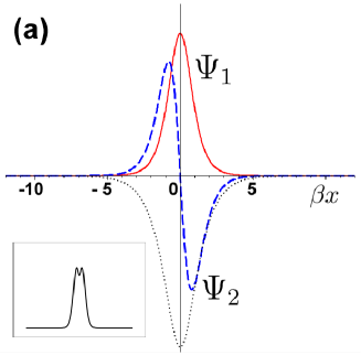
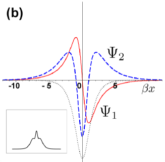
where is the Gamma function. As expected, the two functions given by Eq. (9) are of different parity, thus unlike the non-relativistic case there is an odd function corresponding to the first confined mode. This leads to a threshold in the characteristic potential strength at which the first confined mode appears; much like in the conventional quantum well, where the first odd state appears only for a sufficiently deep or wide potential well. In Fig. 2 we present , and the corresponding electron density profiles for the first and second bound modes for the case of . The shape of the confinement potential is shown for guidance within the same figure. The charge density profile for these modes differs drastically from the non-relativistic case. The first mode () has a dip in the middle of the potential well, whereas the second mode () has a maximum. This is a consequence of the complex two-component structure of the wavefunctions.
For negative values of , and switch parity such that . This means backscattering within a channel requires a change of parity of the wavefunctions in the -direction. Notably, when another non-equivalent Dirac valley is considered, one finds that there are modes of the same parity propagating in the opposite direction. However intervalley scattering requires a very short-range potential or proximity to the sample edges. Thus for smooth scattering potentials backscattering should be strongly suppressed. Such suppression should result in an increase in the mean free path of the channel compared to that of graphene. This is similar to the suppression of backscattering in carbon nanotubes,Ando where the ballistic regime is believed to persist up to room temperature with a mean free path exceeding one micrometer.CNTCombined ; Porntoi_NanoLett_7_2007 In some sense the considered waveguide can be thought of as a carbon nanotube-like structure with parameters controlled by the top gate.
Notably, our results are also applicable for the case of a one-dimensional massive particle which is confined in the same potential. This can be achieved by the substitution into Eqs. (4-5), where the gap is given by . Hence in the massless 2D case the momentum along the waveguide plays the same role as the gap in the massive one-dimensional case. Therefore, in a massive one-dimensional Dirac system (such as a narrow gap carbon nanotube) there exists a bound state in the middle of the gap for certain values of the characteristic strength of the potential.
The number of modes at a fixed value of is the integer part of herein denoted . The conductance of an ideal one-dimensional channel characterized by is found using the Landauer formula to be . By modulating the parameters of the potential, one can increase the conductance of the channel from zero in jumps of . The appearance of the first and further confined modes within the conducting channel modifies both the strength and the profile of the potential. This nonlinear screening effect Fogler_PRL_100_2008 ; Fogler_PRB_77_2008 is neglected in the above expression for and shall be a subject of future investigation.
Exact solutions for confined modes can also be found for the Pöschl-Teller potential, , which corresponds to in Eq. (7). Wavefunctions can be expressed via Heun polynomials in variable .
III Discussion and conclusions
All the results obtained in this paper have been for a specific potential. However, general conclusions can be drawn from these results for any symmetric potential. Namely, the product of the potential strength and its width dictates the number of confined modes within the channel.comment Moreover, this product has a threshold value for which the first mode appears. The width of the potential is defined by the geometry of the top gate structure, and the strength of the potential is defined by the voltage applied to the top gate. The mean free path of electrons within graphene is of the order of 100nm and sub-100nm width gates have been reported in the literature, TopGateCombined ; Kim_PRL_99_2007 ; Savchenko_NanoLett_8_2008 ; Liu_APL_92_2008 ; GG_PRL_102_2009 ; Kim_NatPhys_5_2009 making quantum effects relevant. The number of modes within such top-gated structures is governed by the strength of the potential, with new modes appearing with increasing potential strength. In a top gate structure modeled by our potential with a width at half maximum of 50nm, the first bound mode should appear for a potential strength of approximately 17 meV and further modes should appear with increasing potential strength in steps of 34 meV, which corresponds to 395 K. Therefore a noticeable change in conductivity should be observed in realistic structures even at room temperature. This is similar to the quantum Hall effect which is observed in graphene at room temperature.QHE A change of geometry, from normal transmission to propagation along a potential, allows graphene to be used as a switching device.
In summary, we show that contrary to the widespread belief, truly confined (non-leaky) modes are possible in graphene in a smooth electrostatic potential vanishing at infinity. Full confinement is possible for zero-energy modes due to the vanishing density of states at the charge neutrality point. We present exact analytical solutions for fully confined zero-energy modes in the potential , which provides a good fit (see Appendix) to experimental potential profiles in existing top gate structures. TopGateCombined ; Kim_PRL_99_2007 ; Savchenko_NanoLett_8_2008 ; Liu_APL_92_2008 ; GG_PRL_102_2009 ; Kim_NatPhys_5_2009 Within such a potential there is a threshold value of for which bound modes first appear, which is different to conventional non-relativistic systems. We found a simple relation between the number of confined modes and the characteristic potential strength . The threshold potential strength enables on/off behavior within the graphene waveguide, and suggests future device applications. The existence of bound modes within smooth potentials in graphene may provide an additional argument in favor of the mechanism for minimal conductivity, where charge puddles lead to a percolation network of conducting channels.PercolationNetwork
There are experimental challenges which need to be resolved in order to observe confined modes in graphene waveguides. These include creating narrow gates and thin dielectric layers as well as optimizing the geometry of the sample to reduce the background conductance. Our work also poses further theoretical problems, including the study of non-linear screening, many-body effects, parity changing backscattering and inter-valley scattering within the channel.
The study of quasi-one-dimensional channels within conventional semiconductor systems has lead to many interesting effects. Many problems are still outstanding, including the 0.7 anomaly in the ballistic conductance which is a subject of extensive experimental and theoretical study.1DSystem We envisage that the ability to produce quasi-one-dimensional channels within graphene will reveal new and non-trivial physics.
Acknowledgements.
We are grateful to A.V. Shytov, A.S. Mayorov, Y. Kopelevich, J.C. Inkson, D.C. Mattis and N. Hasselmann for valuable discussions and we thank ICCMP Brasília and UNICAMP for hospitality. This work was supported by EPSRC (RRH and NJR), EU projects ROBOCON (FP7-230832) and TerACaN (FP7-230778), MCT, IBEM and FINEP (Brazil).*
Appendix A Potential due to a wire above a graphene sheet
To illustrate the relevance of our model potential to realistic top-gate structures we provide a simple calculation of the potential distribution in the graphene plane for a simplified top-gate structure. Fig. 3 shows the model that we use for our estimate. We consider a wire of radius , separated by distance from a metallic substrate (i.e. doped Si) and calculate the potential profile in the graphene plane separated from the same substrate by distance . We are interested in the case when the Fermi level in graphene is at zero energy (the Dirac point), hence we assume the absence of free carriers in graphene. We also assume the absence of any dielectric layers, but the problem can be generalized in such an instance.
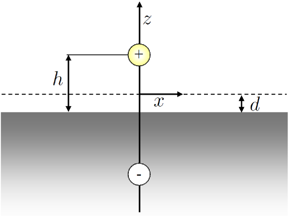
One can easily show that the potential energy for an electron in the graphene plane is given by
| (11) |
where , is the voltage applied between the top electrode and metallic substrate and is the absolute value of the electron charge. One can see that this potential behaves as:
The depth of the potential well is given by
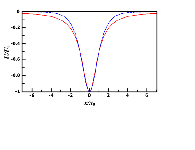
and the half width at half maximum (HWHM) is given by . In Fig. 4 we show a comparison between the potential given by Eq. (11) and the potential considered in our paper with the same HWHM and potential strength. Clearly the potential given by , provides a significantly better approximation than that of the square well potential.
References
- (1) O. Klein, Z. Phys. 53, 157 (1929).
- (2) K. S. Novoselov, A. K. Geim, S. V. Morozov, D. Jiang, M. I. Katsnelson, I. V. Grigorieva, S. V. Dubonos, and A. A. Firsov, Nature (London) 438, 197 (2005).
- (3) A. H. Castro Neto, F. Guinea, N. M. R. Peres, K. S. Novoselov, and A. K. Geim, Rev. Mod. Phys. 81, 109 (2009).
- (4) V. V. Cheianov, V. I. Fal’ko, and B. L. Altshuler, Science 315, 5816 (2007).
- (5) A. V. Shytov, M. S. Rudner, and L. S. Levitov, Phys. Rev. Lett. 101, 156804 (2008).
- (6) L. Zhao and S. F. Yelin, arXiv:0804.2225; Phys. Rev. B 81, 115441 (2010).
- (7) C. W. J. Beenakker, R. A. Sepkhanov, A. R. Akhmerov, and J. Tworzydło, Phys. Rev. Lett. 102, 146804 (2009).
- (8) F. M. Zhang, Y. He, and X. Chen, Appl. Phys. Lett. 94, 212105 (2009).
- (9) M. I. Katsnelson, K. S. Novoselov, and A. K. Geim, Nature Phys. 2, 620 (2006).
- (10) V. V. Cheianov and V. I. Fal’ko, Phys. Rev. B 74, 041403(R) (2006).
- (11) J. M. Pereira Jr., V. Mlinar, F. M. Peeters, and P. Vasilopoulos, Phys. Rev. B 74, 045424 (2006).
- (12) T. Ya. Tudorovskiy and A. V. Chaplik, JETP Lett. 84, 619 (2006).
- (13) J. M. Pereira Jr., P. Vasilopoulos, and F. M. Peeters, Appl. Phys. Lett. 90, 132122 (2007).
- (14) L. M. Zhang and M. M. Fogler, Phys. Rev. Lett. 100, 116804 (2008).
- (15) M. M. Fogler, D. S. Novikov, L. I. Glazman, and B. I. Shklovskii, Phys. Rev. B 77, 075420 (2008).
- (16) C. W. J. Beenakker, Rev. Mod. Phys. 80, 1337 (2008).
- (17) H. C. Nguyen, M. T. Hoang, and V. L. Nguyen, Phys. Rev. B 79, 035411 (2009).
- (18) J. R. Williams, L. DiCarlo, and C. M. Marcus, Science 317, 638 (2007).
- (19) B. Huard, J. A. Sulpizio, N. Stander, K. Todd, B. Yang, and D. Goldhaber-Gordon, Phys. Rev. Lett. 98, 236803 (2007).
- (20) B. Özyilmaz, P. Jarillo-Herrero, D. Efetov, D. A. Abanin, L. S. Levitov, and P. Kim, Phys. Rev. Lett. 99, 166804 (2007).
- (21) R. V. Gorbachev, A. S. Mayorov, A. K. Savchenko, D. W. Horsell, and F. Guinea, Nano Lett. 8, 1995 (2008).
- (22) G. Liu, J. Velasco Jr., W. Bao, and C. N. Lau, Appl. Phys. Lett. 92, 203103 (2008).
- (23) N. Stander, B. Huard, and D. Goldhaber-Gordon, Phys. Rev. Lett. 102, 026807 (2009).
- (24) A. F. Young and P. Kim, Nature Phys. 5, 222 (2009).
- (25) M. Y. Han, B. Özylimaz, Y. Zhang, and P. Kim, Phys. Rev. Lett. 98, 206805 (2007).
- (26) L. Brey and H. A. Fertig, Phys. Rev. B 73, 235411 (2006).
- (27) P. G. Silvestrov and K. B. Efetov, Phys. Rev. Lett. 98, 016802 (2007).
- (28) N. M. R. Peres, J. N. B. Rodrigues, T. Stauber, and J. M. B. Lopes dos Santos, J. Phys.: Condens. Matter 21, 344202 (2009).
- (29) D, W. Horsell, A. K. Savchenko, F. V. Tikhonenko, K. Kechedzhi, I. V. Lerner, and V. I. Fal ko, Solid State Commun. 149, 1041 (2009).
- (30) Y. -W. Tan, Y. Zhang, K. Bolotin, Y. Zhao, S. Adam, E. H. Hwang, S. Das Sarma, H. L. Stormer, and P. Kim, Phys. Rev. Lett. 99, 246803 (2007).
- (31) P. M. Ostrovsky, I. V. Gornyi, and A. D. Mirlin, Phys. Rev. Lett. 98, 256801 (2007).
- (32) S. Adam, E. H. Hwang, V. M. Galitski, and S. Das Sarma, Proc. Natl. Acad. Sci. USA 104, 18392 (2007).
- (33) V. V. Cheianov, V. I. Fal’ko, B. L. Altshuler, and I. L. Aleiner, Phys. Rev. Lett. 99, 176801 (2007).
- (34) M. I. Katsnelson, Eur. Phys. J. B 51, 157 (2006).
- (35) J. Tworzydło, B. Trauzettel, M. Titov, A. Rycerz, and C. W. J. Beenakker, Phys. Rev. Lett. 96, 246802 (2006).
- (36) G. Pöschl and E. Teller, Z. Phys. 83, 143 (1933).
- (37) T. Ando, T. Nakanishi and R. Saito, J. Phys. Soc. Japan 67, 2857 (1998).
- (38) M. P. Anantram and F. Léonard, Rep. Prog. Phys. 69, 507 (2006).
- (39) O. V. Kibis, M. Rosenau da Costa, and M. E. Portnoi, Nano Lett. 7, 3414 (2007) and references therein.
- (40) For example, in a finite square well of width and depth , new zero-energy states appear when , where
- (41) K. S. Novoselov, Z. Jiang, Y. Zhang, S. V. Morozov, H. L. Stormer, U. Zeitler, J. C. Maan, G. S. Boebinger, P. Kim, and A. K. Geim, Science 315, 1379 (2007).
- (42) I. A. Shelykh, M. Rosenau da Costa, and A. C. Seridonio, J. Phys.: Condens. Matter 20, 164214 (2007) and references therein.