Theory and design of quantum cascade lasers in (111) -type Si/SiGe
Abstract
Although most work towards the realization of group IV quantum cascade lasers (QCLs) has focused on valence band transitions, there are many desirable properties associated with the conduction band. We show that the commonly cited shortcomings of -type Si/SiGe heterostructures can be overcome by moving to the (111) growth direction. Specifically, a large band offset and low effective mass are achievable and subband degeneracy is preserved. We predict net gain up to lattice temperatures of 90 K in a bound-to-continuum QCL with a double-metal waveguide, and show that a Ge interdiffusion length of at least 8 Å across interfaces is tolerable.
pacs:
73.43.Cd, 73.61.Cw, 78.45.+h, 78.67.PtI Introduction
Quantum cascade lasers (QCLs) have been developed in a variety of III-V materials systems, although as yet there has been no successful demonstration in group IV. A Si/SiGe QCL would potentially reduce fabrication costs and offer a route to photonic system-on-a-chip applications.Kelsall et al. (2003)
The most common approach towards a Si/SiGe QCL uses (001) oriented -type structures,Kelsall et al. (2003) and electroluminescenceDehlinger et al. (2000); Paul et al. (2003); Lynch et al. (2002) has been demonstrated. There are however significant challenges in designing -type QCLs. The coexistence of heavy and light holes leads to fast nonradiative scattering, and strong valence band mixing causes large variations in transition energies and matrix elements with in-plane wave vector.Ikonić et al. (2001)
The high longitudinal effective mass of SiGe valleys is commonly regarded as a major obstacle to -type QCLs,Paul (2004) and recent theoretical investigations have used transitions in the and valleys instead.Han and Yu (2007); Driscoll and Paiella (2006) We have however shown previously that a (111) oriented Si/SiGe QCL using valley transition is viable.Lever et al. (2008)
In this paper, we compare the strain tensors for (001) and (111) oriented layers. We show that (111) oriented valleys offer larger usable band offsets and lower quantization effective mass than the (001) case and that complications due to subband degeneracy splitting are avoided. We summarize our calculations of the principal scattering mechanisms, current and gain, and present a bound-to-continuum QCL design in -type (111) Si/SiGe. We calculate the waveguide losses and predict net gain in our design. Finally, we investigate the effects of temperature and nonabrupt interfaces.
II Strain tensors
Lattice mismatch induces strain in thin Si1-xGex layers on a relaxed SiGe substrate, where . Layers below their critical thickness deform elastically to match the in-plane lattice constant of the substrate and strain balancing of a multilayer structure is required to achieve mechanical stability. This is achieved by selecting a substrate alloy which minimizes elastic potential energy with respect to in-plane strain.Harrison (2005) It is convenient to convert between both the interface coordinate system , where the axis is normal to the layer interfaces, and the crystallographic coordinate system . For the (001) case, , whereas for (111) systems a transformation matrix is required.Hinckley and Singh (1990)
The in-plane strain in is defined as
| (1) |
where is the lattice constant of the unstrained layer and is that of the substrate. A good approximation for lattice constant (in nm) isBublik et al. (1974)
| (2) |
Assuming isotropy over the plane, the strain tensors in for (001) and (111) oriented layers areSmirnov and Kosina (2004)
| (3) |
| (4) |
where are the elastic constants, and .
The minimum average strain energy corresponds to a substrate lattice constant,Harrison (2005)
| (5) |
where is the layer thickness, is the layer index and the elastic constants are grouped into a single term . For the (001) and (111) orientations, the elastic constants are
| (6) |
| (7) |
III Band structure

As QCLs are intersubband devices, the indirect Si1-xGex bandgap is not an obstacle. The effective mass model for SiGe-based systems however, must account for transitions occurring away from the symmetry point. The band structure is described as follows.
III.1 Unstrained valley potential
The unstrained conduction band minima in Si1-xGex with % are located in six degenerate valleys in space. Each valley lies close to an symmetry point, and has a spheroidal equipotential surface with its major axis along the associated direction.Davies (1998)
The relaxed valley potential relative to the substrate is determined from the model solid approximation.Van de Walle (1989) The difference in average valence band maximum (in eV) is
| (8) |
and the highest valence band maximum is one third of the spin-orbit splitting above this, such that
| (9) |
where is the difference in spin orbit splitting between the two materials.Van de Walle (1989)
The unstrained valley conduction band offset is therefore
| (10) |
where is the difference in indirect bandgap. To a good approximation, this is given (in eV) byWeber and Alonso (1989)
| (11) |
III.2 Strained layers
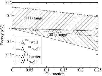
In general, two strain dependent terms are added to Eqn. 10. Firstly, hydrostatic strain, i.e. the overall volume change, shifts the potential by an amount , where is the hydrostatic conduction band deformation potential. For (001) heterostructures, the hydrostatic shift is
| (12) |
whereas for (111) heterostructures, it is
| (13) |
Secondly, uniaxial strain, i.e. the distortion from the cubic lattice form, splits the in-plane and the perpendicular valley potentials by an amount
| (14) |
where is the uniaxial deformation potential. The upper sign represents the valleys and the lower sign represents . This effect is absent in (111) heterostructures as strain is identical along each of the principal crystallographic axes.
The calculation is summarized in Fig. 1. The conduction band edge is generally shifted by hydrostatic strain, and in the (001) orientation, uniaxial strain splits the valley degeneracy. Although intervalley optical transitions are forbidden by the wave vector shift, degeneracy splitting complicates (001) QCL design by introducing nonradiative transitions. It is therefore desirable to restrict optical transitions to energies below the valley minima.
For a strain balanced QCL with barriers narrower than wells, . Fig. 2 shows that the usable energy range in the (001) orientation decreases almost linearly with from a maximum of 150 meV at =25%. The (111) orientation is therefore desirable for QCL designs as the entire offset of 150 meV may be used regardless of the substrate composition.
III.3 Effective mass
| Valley | |||
|---|---|---|---|
| =0.19 | =0.42 | 4 | |
| =0.916 | = 0.19 | 2 | |
| =0.26 | =0.36 | 6 |
The spheroidal valley approximation remains valid in strained SiGe, as the effective mass only varies slightly.Rieger and Vogl (1993) However, two separate effective masses are required: the longitudinal effective mass =0.916 for wave vectors along the major axis of a valley and the transverse effective mass =0.19 for wave vectors along the minor axes. The conduction band energy near a valley minimum is
| (15) |
where are constant effective masses for momentum in a given direction in , and is the wave vector relative to the subband minimum.
In QCLs, the quantization effective mass describes the variation of conduction band potential in the growth direction, i.e. . The density-of-states mass accounts for in-plane motion and is anisotropic with respect to the in-plane wave vector. An isotropic approximation, is commonly used however.Schenk (1996); Mizuno et al. (1993) The effective mass values are summarized in Tbl. 1.
In the (001) orientation, the major axes of all four valleys lie in-plane, so and . Conversely, the major axis of each valley points in the growth direction, so , while is isotropic and equal to .
It is slightly inaccurate to treat the subbands as being twofold degenerate in a simple effective mass approximation (EMA) as intervalley mixing splits the degeneracy in quantum confined systems.Ohkawa and Uemura (1977) We have accounted for this in symmetric systems in a modified EMA and shown that the effect may be large in narrow quantum wells.Valavanis et al. (2007) However, asymmetric structures require a computationally expensive atomistic calculation.Boykin et al. (2004); Friesen et al. (2007) As the splitting is at most a few meV in weakly confined states, the effect was neglected in the QCL simulations presented in this work.
In (111) heterostructures, the situation is much simpler. All six valleys have and identical confining potentials. Intervalley mixing is absent as each valley lies at a different value of . The subbands are therefore sixfold degenerate within the EMA.
In summary, the conduction band for (001) heterostructures is complicated by effective mass anisotropy. The subbands may conceivably be used for QCL design, but the large value severely limits the oscillator strength and hence the gain.Davies (1998) The subbands have lower , but states are weakly confined by the small band offsets and have low populations due to their high energy.
The (111) orientation however, offers both low effective mass and high band offset and shows more promise for QCL designs. The low mass allows wider wells to be used than for transitions in (001) systems. QCL designs in the (111) orientation are therefore more tolerant to deviations in layer thicknesses caused by growth errors.
IV Carrier transport model
Having established the differences in band structure and effective mass between (001) and (111) oriented heterostructures, carrier transport may now be modeled in QCL structures. Detailed quantum theoretical approaches have been used to simulate intersubband optical emissions in quantum wellsWaldmüller et al. (2004) and carrier transport in limited numbers of subbands in QCLs.Lee and Wacker (2002) They are, however, too computationally demanding for use as design tools for large multi-level QCLs.
Reasonably good agreement has been achieved between experimental results and Boltzmann or rate equation based models of bound-to-continuum THz QCLs in III–V systems.Köhler et al. (2002); Jovanovic et al. (2006) In the present work, we have therefore determined subband populations using a computationally efficient rate equation approach.Jovanovic et al. (2006) This has been described in more detail previously,Valavanis et al. (2008) although a brief summary follows.
Several intravalley scattering mechanisms are important in Si/SiGe systems. Interface roughness scattering was calculated using the correlated Gaussian roughness model,Ando et al. (1982) modified for arbitrary interface geometriesValavanis et al. (2008) and alloy disorder scattering was calculated using a point perturbation model.Quang et al. (2007); Murphy-Armando and Fahy (2006) Ionized impurity scattering was determined using a Coulombic interaction model as described by UnumaUnuma et al. (2003) with Thomas-Fermi screening,Davies (1998) while electron-electron scattering was treated as a screened Coulombic interaction as described by Smet.Smet et al. (1996) The intravalley deformation potential scattering for electron-acoustic phonon interactions was also included.
Intervalley electron-phonon scattering was determined only for the Si-Si branch of the deformation potential interaction, as the Ge fraction in quantum wells is small. The processes, which transfer electrons to the perpendicular valleys, are faster than processes which transfer electrons to the opposite valley, due to the larger number of destination states.Canali et al. (1975) Of the processes, the -LA (phonon energy = 46.3 meVDollfus (1997)) and -TO ( = 59.1 meVDollfus (1997)) interactions are rapid zero-order terms in the scattering model.Monsef et al. (2002) Scattering rates increase rapidly with transition energy, and saturate above the phonon energy.
The electron transfer rate from initial subband to final subband is the product of the average intersubband scattering rate (due to all scattering processes) and the initial subband population . Although a simple estimate of current density is proportional to the total electron transfer rate,Ikonic et al. (2004) an improved model takes account of the spatial separation of electrons. The current density is therefore
| (16) |
where is the electronic charge, is the length of a structural period and is the expectation value of the position operator.
The active region gain or absorption for each transition was calculated asJovanovic et al. (2006)
| (17) |
where is the refractive index of Si, is the permittivity of free space, and is the speed of light in vacuo. is the energy difference between the subband minima, is the signum function, is the dipole matrix element, and is the lineshape for the transition. The gain spectrum is found by summing Eqn. 17 over all transitions.
Although linewidth may be obtained directly from our scattering rate calculations,Unuma et al. (2003) or from more sophisticated models,Waldmüller et al. (2004) several important implementation issues, such as how to treat the extremely broad absorptions into weakly bound higher energy subbands, are beyond the scope of the present work. Normalized Lorentzian lineshapes centered about have been observed in THz III-V systems, with full-width at half-maximum around 2 meV at low temperatures.Köhler et al. (2002) We therefore calculated gain spectra using linewidths in the range 1.5–2.5 meV. At higher lattice temperatures, the increased scattering rates cause linewidth broadening,Waldmüller et al. (2004); Page et al. (2001) and consequently we expect our higher linewidth results to be more realistic at higher temperatures.
V QCL performance
We have described the advantages of the (111) orientation for Si/SiGe QCLs in general terms and have previously predicted net gain in a novel phonon depopulation QCL.Lever et al. (2008) In this section, we present a bound-to-continuum active region design with a double-metal waveguide and demonstrate that net gain is achievable up to 90 K. We also show that reasonable limitations in growth quality due to interdiffusion do not present a significant obstacle.
V.1 Active region design
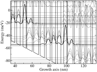
The band structure in a seven-well bound-to-continuum QCL was calculated using a single band EMA and is shown in Fig. 3 for a 7 kVcm-1 applied electric field. Non-radiative depopulation of the upper laser subband was reduced by limiting the higher energy scattering processes. Pure Si wells were used to minimize alloy disorder scattering, and a relatively low Ge composition of 40% was selected for the barriers to reduce interface roughness scattering. The optical transition energy was chosen to be significantly smaller than 46.3 meV to reduce -LA and -TO phonon emission rates.
As modulation doping of donors in Si/SiGe heterostructures may be difficult,Zhang et al. (2006) dopants were assumed to be spread evenly throughout the structure. It was also assumed that all donors were ionized at low temperatures. A donor concentration of cm-3 (sheet doping density of cm-2) caused negligible internal electric fields, while still allowing rapid depopulation of upper miniband states by Coulombic scattering.
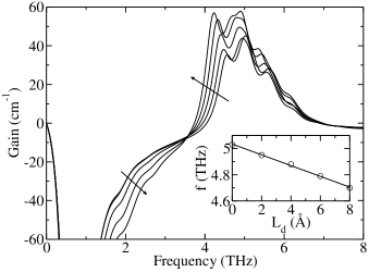
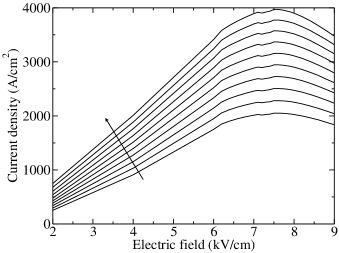
Figure 5 shows gain at frequencies around 5 THz, due to transitions from the upper laser subband to upper miniband states, for 4 K lattice temperature and 7 kVcm-1 applied electric field. Figure 4 shows that a current density of 2 kAcm-1 corresponds to these conditions, and doubles as lattice temperature increases to 100 K. An energy balance approachJovanovic et al. (2006) was used to find electron temperatures. Assuming an identical temperature in each subband, we found that electron temperatures increased from 110 to 150 K as lattice temperatures increased from 4 to 100 K.
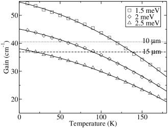
Figure 6 shows the peak gain near 5 THz as a function of lattice temperature for 1.5, 2.0 and 2.5 meV transition linewidths. As discussed in section IV, linewidth increases with temperature, and we expect the low-temperature gain to be enhanced and the high-temperature gain to be limited accordingly.
To provide a fair comparison with subbands in the (001) orientation, an equivalent (001) design was developed. Firstly, the conduction band offset was matched to that of the (111) design by setting the barrier Ge fraction to 26%. Noting that the subband energies are much smaller than the barrier energy, an infinite quantum well approximation was used to transform the layer widths and preserve subband separation,
| (18) |
This scaling also preserves the barrier transparency, i.e. the coupling between adjacent wells. Finally, the applied electric field was increased to 13.1 kVcm-1 to account for the reduced period length.
The subbands in the (001) system were at sufficiently low energy compared with the valleys, for -phonon interactions to be negligible. With the larger electric field, and with only slow -phonon interactions available to cool the electron distribution, the steady-state electron temperature was greatly increased to 290 K for a lattice temperature of 4 K. Consequently, thermal backscattering led to a much lower peak gain coefficient of 0.2 cm-1 at 6 THz, corresponding to a current density of 1.1 kAcm-1. Growth of such a structure is also expected to be challenging, as the minimum layer thickness was reduced to 4 Å.
V.2 Waveguide design
A suitable waveguide was designed using a one-dimensional simulation. The propagation constant was obtained using a transfer matrix methodAnemogiannis et al. (1999) and the complex permittivities were found using the bulk Drude model using Si/SiGe material parameters from Ref. Palankovski, 2000. The active region was modelled as bulk Si0.9Ge0.1 (to match the virtual substrate), with a doping concentration of cm-3.
Surface-plasmon configurationsKöhler et al. (2002) were found to be unsuitable, due to the low confinement factor and large waveguide losses . We therefore chose a metal-metal configuration, which has proved successful in GaAs-based THz QCLs.Williams et al. (2003) The active region was enclosed between a pair of highly doped ( cm-3), 20 nm thick Si layers, followed by the metallic layers. The optical properties of the metallic layers are given in Ref. Ordal et al., 1985.
An initial design, using gold metallic layers and a 10 m thick active region gave =50.7 cm-1 and =0.99. Assuming mirror losses of = 1 cm-1,Kohen et al. (2005) the threshold gain was determined as cm-1, which was too high to achieve lasing.
The highest temperature operation of a GaAs-based THz QCL was achieved recently by using copper instead of gold layers.Belkin et al. (2008) Incorporating this into our waveguide reduces the threshold gain to 40.5 cm-1. As shown in Fig. 6, this permits lasing up to T=58 K for a 2 meV linewidth. By increasing the active region thickness to 15 m, the threshold gain was reduced further to 36.9 cm-1, which permits lasing up to T=90 K.
V.3 Growth variations
We restricted our (111) design to layer thicknesses above 8 Å as Si/SiGe epitaxy is not as well established as in III-V systems. The thinnest barrier would ideally be thinner than this to increase the dipole matrix element between the bound subband and the upper miniband states. The requirement for thin barriers is less important in (111) heterostructures than in (001) however, as the quantization effective mass is smaller and the matrix element is larger.
Ge surface segregation has been observed in (001) heterostructures,Zhang et al. (2006) and presumably this will also be the case in (111) systems. The geometry of the thinnest layers in a QCL is expected to change considerably as a result. We have previously shown however, that a limited amount of interdiffusion is tolerable, although changes in transition energies are expected.Valavanis et al. (2008)
Figure 5 shows that gain increases slightly as a function of interdiffusion length, up to 8 Å for our QCL design. This is due to the thinnest barrier being degraded, increasing the dipole matrix element for optical transitions. The inset in the figure shows that the center of the largest gain peak correspondingly shifts from around 5 to 4.7 THz, as the upper laser subband energy decreases.Valavanis et al. (2008)
VI Conclusion
We have shown that intersubband lasing in the valleys of Si/SiGe heterostructures becomes viable in the (111) orientation. Although the conduction band offset in the (001) orientation is large, the usable energy range was shown to be superior in the (111) orientation due to the sixfold valley degeneracy. The quantization effective mass was also shown to be much smaller in (111) heterostructures, and complications due to intervalley mixing and uniaxial strain splitting are avoided.
We have presented a bound-to-continuum design for a (111) Si/SiGe QCL and investigated several options for waveguides. A surface-plasmon waveguide was shown to be inadequate, while good results were achieved for a double-metal configuration using copper metallic layers. We have shown using a self-consistent rate-equation/energy balance calculation that net gain at 5 THz is possible up to a lattice temperature of 90 K, with a low-temperature current density of 2 kAcm-1 for a 15 m thick active region.
The (111) design was found to be vastly superior to a (001) oriented equivalent, due to the phonon-mediated electron cooling and the reduced effective mass. It was also shown to be tolerant to, and indeed improve slightly, with Ge interdiffusion lengths up to 8 Å.
Acknowledgements.
This work is supported by EPSRC Doctoral Training Allowance funding and DTI-MNT contract 491: “Fast THz Cameras”.References
- Kelsall et al. (2003) R. W. Kelsall, Z. Ikonić, P. Harrison, S. A. Lynch, R. Bates, D. J. Paul, D. J. Norris, S. L. Liew, A. G. Cullis, D. J. Robbins, et al., in Towards the First Silicon Laser, edited by L. Pavesi, S. Gaponenko, and L. D. Negro (Kluwer Academic Publishers, Dordrecht, 2003), vol. 93 of NATO Science Series II: Mathematics, Physics and Chemistry, pp. 367–382.
- Dehlinger et al. (2000) G. Dehlinger, L. Diehl, U. Gennser, H. Sigg, J. Faist, K. Ensslin, D. Grutzmacher, and E. Muller, Science 290, 2277 (2000).
- Paul et al. (2003) D. Paul, S. Lynch, R. Bates, Z. Ikonić, R. Kelsall, P. Harrison, D. Norris, S. Liew, A. Cullis, D. Arnone, et al., Physica E 16, 147 (2003).
- Lynch et al. (2002) S. A. Lynch, R. Bates, D. J. Paul, D. J. Norris, A. G. Cullis, Z. Ikonic, R. W. Kelsall, P. Harrison, D. D. Arnone, and C. R. Pidgeon, Appl. Phys. Lett. 81, 1543 (2002).
- Ikonić et al. (2001) Z. Ikonić, P. Harrison, and R. W. Kelsall, Phys. Rev. B 64, 245311 (2001).
- Paul (2004) D. J. Paul, Semicond. Sci. Tech. 19, R75 (2004).
- Han and Yu (2007) G. Han and J. Yu, Semicond. Sci. Tech. 22, 769 (2007).
- Driscoll and Paiella (2006) K. Driscoll and R. Paiella, Appl. Phys. Lett. 89, 191110 (2006).
- Lever et al. (2008) L. Lever, A. Valavanis, Z. Ikonić, and R. W. Kelsall, Appl. Phys. Lett. 92, 021124 (2008).
- Harrison (2005) P. Harrison, Quantum Wells, Wires and Dots (Wiley, Chichester, 2005), 2nd ed.
- Hinckley and Singh (1990) J. M. Hinckley and J. Singh, Phys. Rev. B 42, 3546 (1990).
- Bublik et al. (1974) V. Bublik, S. Gorelik, A. Zaitsev, and A. Polyakov, Phys. Status Solidi 65, K79 (1974).
- Smirnov and Kosina (2004) S. Smirnov and H. Kosina, Solid State Electron. 48, 1325 (2004).
- Davies (1998) J. H. Davies, The Physics of Low-Dimensional Semiconductors: An Introduction (Cambridge University Press, Cambridge, 1998).
- Van de Walle (1989) C. G. Van de Walle, Phys. Rev. B 39, 1871 (1989).
- Rieger and Vogl (1993) M. M. Rieger and P. Vogl, Phys. Rev. B 48, 14276 (1993).
- Weber and Alonso (1989) J. Weber and M. I. Alonso, Phys. Rev. B 40, 5683 (1989).
- Rahman et al. (2005) A. Rahman, M. S. Lundstrom, and A. W. Ghosh, J. Appl. Phys. 97, 053702 (2005).
- Schenk (1996) A. Schenk, J. Appl. Phys. 79, 814 (1996).
- Mizuno et al. (1993) H. Mizuno, K. Taniguchi, and C. Hamaguchi, Phys. Rev. B 48, 1512 (1993).
- Ohkawa and Uemura (1977) F. J. Ohkawa and Y. Uemura, J. Phys. Soc. Jpn. 43, 907 (1977).
- Valavanis et al. (2007) A. Valavanis, Z. Ikonić, and R. W. Kelsall, Phys. Rev. B 75, 205332 (2007).
- Boykin et al. (2004) T. B. Boykin, G. Klimeck, M. Friesen, S. N. Coppersmith, P. von Allmen, F. Oyafuso, and S. Lee, Phys. Rev. B 70, 165325 (2004).
- Friesen et al. (2007) M. Friesen, S. Chutia, C. Tahan, and S. N. Coppersmith, Phys. Rev. B 75, 115318 (2007).
- Waldmüller et al. (2004) I. Waldmüller, J. Förstner, S.-C. Lee, A. Knorr, M. Woerner, K. Reimann, R. A. Kaindl, T. Elsaesser, R. Hey, and K. H. Ploog, Phys. Rev. B 69, 205307 (2004).
- Lee and Wacker (2002) S.-C. Lee and A. Wacker, Phys. Rev. B 66, 245314 (2002).
- Köhler et al. (2002) R. Köhler, A. Tredicucci, F. Beltram, H. E. Beere, E. H. Linfield, A. G. Davies, D. A. Ritchie, R. C. Iotti, and F. Rossi, Nature 417, 156 (2002).
- Jovanovic et al. (2006) V. D. Jovanovic, S. Hofling, D. Indjin, N. Vukmirovic, Z. Ikonic, P. Harrison, J. P. Reithmaier, and A. Forchel, J. Appl. Phys. 99, 103106 (2006).
- Valavanis et al. (2008) A. Valavanis, Z. Ikonić, and R. W. Kelsall, Phys. Rev. B 77, 075312 (2008).
- Ando et al. (1982) T. Ando, A. B. Fowler, and F. Stern, Rev. Mod. Phys. 54, 437 (1982).
- Quang et al. (2007) D. N. Quang, N. H. Tung, D. T. Hien, and H. A. Huy, Phys. Rev. B 75, 073305 (2007).
- Murphy-Armando and Fahy (2006) F. Murphy-Armando and S. Fahy, Phys. Rev. Lett. 97, 096606 (2006).
- Unuma et al. (2003) T. Unuma, M. Yoshita, T. Noda, H. Sakaki, and H. Akiyama, J. Appl. Phys. 93, 1586 (2003).
- Smet et al. (1996) J. H. Smet, C. G. Fonstad, and Q. Hu, J. Appl. Phys. 79, 9305 (1996).
- Canali et al. (1975) C. Canali, C. Jacoboni, F. Nava, G. Ottaviani, and A. Alberigi-Quaranta, Phys. Rev. B 12, 2265 (1975).
- Dollfus (1997) P. Dollfus, J. Appl. Phys. 82, 3911 (1997).
- Monsef et al. (2002) F. Monsef, P. Dollfus, S. Galdin, and A. Bournel, Phys. Rev. B 65, 212304 (2002).
- Ikonic et al. (2004) Z. Ikonic, P. Harrison, and R. W. Kelsall, J. Appl. Phys. 96, 6803 (2004).
- Page et al. (2001) H. Page, C. Becker, A. Robertson, G. Glastre, V. Ortiz, and C. Sirtori, Appl. Phys. Lett. 78, 3529 (2001).
- Zhang et al. (2006) J. Zhang, S. Turner, S. Chiam, R. Liu, E. Tok, A. Wee, A. Huan, I. Kelly, and C. Mulcahy, Surf. Sci. 600, 2288 (2006).
- Anemogiannis et al. (1999) E. Anemogiannis, E. Glytsis, and T. Gaylord, J. Lightwave Technol. 17, 929 (1999).
- Palankovski (2000) V. Palankovski, Ph.D. thesis, Technischen Universität Wien (2000).
- Williams et al. (2003) B. S. Williams, S. Kumar, H. Callebaut, Q. Hu, and J. L. Reno, Appl. Phys. Lett. 83, 2124 (2003).
- Ordal et al. (1985) M. A. Ordal, R. J. Bell, J. R. W. Alexander, L. L. Long, and M. R. Querry, Appl. Opt. 24, 4493 (1985).
- Kohen et al. (2005) S. Kohen, B. S. Williams, and Q. Hu, J. Appl. Phys 97, 053106 (2005).
- Belkin et al. (2008) M. A. Belkin, J. A. Fan, S. Hormoz, F. Capasso, S. P. Khanna, M. Lachab, A. G. Davies, and E. H. Linfield, Opt. Express 16, 3242 (2008).