Intersubband carrier scattering in - and -Si/SiGe quantum wells with diffuse interfaces
Abstract
Scattering rate calculations in two-dimensional Si/Si1-xGex systems have typically been restricted to rectangular Ge profiles at interfaces between layers. Real interfaces however, may exhibit diffuse Ge profiles either by design or as a limitation of the growth process. It is shown here that alloy disorder scattering dramatically increases with Ge interdiffusion in (100) and (111) -type quantum wells, but remains almost constant in (100) -type heterostructures. It is also shown that smoothing of the confining potential leads to large changes in subband energies and scattering rates and a method is presented for calculating growth process tolerances.
pacs:
73.50.Bk, 73.21.Fg, 73.63.Hs, 73.61.CwI Introduction
Two dimensional intersubband devices in the Si/Si1-xGex materials system offer a possible reduction in fabrication costs compared with more conventional III–V systems.Pavesi et al. (2003) Successful operation of resonant tunneling diodes (RTDs) has been achievable for several years,Liu et al. (1988) and electroluminescence from more complex quantum cascade structures has been observed.Dehlinger et al. (2000); Bates et al. (2003) A quantum cascade laser (QCL) has not yet been developed in Si/Si1-xGex although several designs have been proposed recently.Driscoll and Paiella (2006); Han and Yu (2007)
In order to accurately design and simulate such structures, a good understanding of intersubband carrier dynamics is required. Previous models have assumed that interfaces between layers are perfectly abrupt,Ikonic et al. (2004) while in reality, diffuse Ge profiles may result either by design, by interdiffusion during the growth process or by surface segregation of Ge atoms.Zhang et al. (2006)
The Ge interdiffusion dramatically changes the subband spacingLi et al. (1996) and the overlap between wave functions. A more accurate model of intersubband scattering rates must therefore account for these effects. In this paper, we review the models of the principal intersubband scattering rates and extend the conventional interface roughness scattering model to an arbitrary interface geometry. To determine the effect on simple intersubband systems, scattering rates were calculated as a function of subband spacing, electron temperature, and diffusion length in single quantum wells (QWs) in (100) -type and (100) and (111) -type systems.
Knowing the effect of interdiffusion on scattering rate, it is possible to estimate the robustness of device designs. By calculating intersubband scattering rates and subband spacings, design tolerance to interdiffusion may be estimated. The viability of a design may be assessed by comparing this with the capabilities of growth processes. We use the example of a coupled QW system to demonstrate the technique and predict the level of interdiffusion required to cause device failure.
II Scattering models
Carrier scattering in a two dimensional Si/Si1-xGex system may be described by a set of independent processes. The models for the Coulombic, electron–phonon, and alloy disorder interactions apply to arbitrary interface geometries, while some modification is required for interface roughness scattering. The mechanisms are summarized as follows.
II.1 Interface roughness scattering
In -confined two-dimensional heterostructures, the confining potential varies with fluctuations in interface location over the plane.Prange and Nee (1968); Penner et al. (1998) The roughness is usually assumed to have a Gaussian Fourier transform with height and correlation length , which is isotropic across the plane,Sakaki et al. (1987); Tsujino et al. (2005); Ando et al. (1982) such that
| (1) |
The commonly used expression for the resulting scattering rateUnuma et al. (2003) assumes an abrupt interface geometry. This has been accurately fitted to experimental data for structures with approximately abrupt interfaces,Califano et al. (2007) but the expression is incompatible with smooth envelope potentials. We determine the scattering rate for an arbitrary interface geometry and verify that it reduces to the specific case of an abrupt interface.
The perturbation due to a position shift in an arbitrary confining potential is assumed to be correlated over the length of a single interface. At the point assuming isotropy across the plane,
| (2) |
If the -th interface in a multilayer structure is centered about the plane and extends over the range , we define the scattering matrix element as
| (3) |
where and are the final and initial wave functions respectively and the rectangular function is defined as
| (4) |
From Fermi’s golden rule, the scattering rate isUnuma et al. (2003)
| (5) |
where is the scattering vector, and are the final and initial wave vectors respectively, is the scattering angle and is the density-of-states effective mass.
At this stage, the general result may be tested against the example of an abrupt change in envelope potential of magnitude , where the perturbating potential is
| (6) |
Under time-independent perturbation theory, the perturbation must be small, i.e. and the perturbing potential simplifies to
| (7) |
The scattering matrix element (Eqn. 3) becomes
| (8) |
in agreement with the well known expression.Unuma et al. (2003)
Returning now to the general expression for scattering rate (Eqn. 5), we determine the total scattering rate for a structure with layers, numbered . The integral over simplifies to a regular modified cylindrical Bessel function of zeroth order, .Gradshteyn and Ryzhik (2000) By assuming roughness profiles are uncorrelated over separate interfaces, the total rate is found as a summation,
| (9) |
where the Heaviside step function, permits a nonzero rate only for real final wave vectors. The new matrix element is
| (10) |
where .
The new model was fitted to the experimental data described in detail in our previous paper.Califano et al. (2007) The parameters, {=1.4 Å, =50 Å} accurately fit the measurements and are very similar to our previous theoretical values,Califano et al. (2007) and to other recent data.Huan and Hai (2007); Tsujino et al. (2005) The slight difference in fitting parameters arises from numerical approximations in the perturbing potentials: the perturbation for arbitrary interface geometries (Eqn. 2) uses a Taylor series expansion, whereas the solution for abrupt interfaces (Eqn. 7) uses the Dirac function limit of the narrow rectangular function.
II.2 Alloy disorder scattering
A standard scattering model for alloy disorder scattering,Quang et al. (2007); Murphy-Armando and Fahy (2006) has been modified slightly to permit variable alloy composition, . The resulting scattering potential becomes
| (11) |
where is the in-plane lattice constant and is commonly approximated as the difference in conduction band potentials between Si and Ge. As for a pure Si layer, the integral domain in abrupt interface systems is restricted to the barriers in -type systems or the wells in -type systems. In a diffuse system however, the Ge content is always nonzero and the integral domain extends over the entire structure.
II.3 Carrier–phonon scattering
Wells in -type heterostructures contain similar fractions of Si and Ge. Hole–phonon scattering via the deformation potential interaction was therefore calculated for the Si–Si, Si–Ge, and Ge–Ge branches of the nonpolar optical mode.Ikonić et al. (2001); Ikonic et al. (2004) In -type heterostructures however, the Ge fraction in the wells is small and only the Si–Si branch was considered. Intravalley deformation potential scattering for the acoustic mode was included for both - and -type heterostructures.
In -type, Si-rich systems, scattering between conduction band valleys is described by either processes, which transfer electrons to the opposite valley in reciprocal space or processes which transfer electrons to the four perpendicular valleys.Canali et al. (1975) -LO, -LA, and -TO interactions are permitted in a zero-order model, whereas -LA, -TA, and -TA interactions are permitted only as first-order processes Monsef et al. (2002) and are somewhat slower. The interactions are characterized by a deformation potential and a frequency, , which for intervalley interactions is nonzero. The scattering rates increase rapidly with subband separation, until they saturate at .
II.4 Coulombic interactions
Ionized impurity scattering and carrier–carrier scattering rates were calculated as Coulombic interactions between either a carrier and a dopant ion or a pair of carriers. The expression for ionized impurity scattering given by Unuma,Unuma et al. (2003) was modified to incorporate static screening in the Thomas-Fermi approximation.Davies (1998) Carrier–carrier scattering rates were calculated using the screened Coulombic interaction model described by Smet et. al.Smet et al. (1996) Both rates are fastest for transitions between energetically similar states. Doping was set as 1 cm-3 throughout each structure we considered, as modulation doping is difficult to achieve in SiGe heterostructures.Zhang et al. (2006) We also assume that all dopants are ionized at low temperatures. The sheet doping density was calculated as the product of the total volume doping and the length of the structure.
II.5 Average rates
As justified previously,Jovanovic et al. (2006) all subband electron temperatures were set to a single average value, , assumed to be different from the lattice temperature, which was taken as =4 K in our calculations. The average scattering rate from the second to first subband, was calculated as
| (12) |
where intrasubband scattering was assumed to be much faster than intersubband. The initial distribution of electrons is therefore an equilibrium Fermi-Dirac function, using the quasi-Fermi level for the subband, where is the initial wave vector. The assumption has also been made that the destination states are always unoccupied, which is reasonable at low doping levels.
III Diffuse quantum wells
Annealing of an abrupt structure, with the Ge fraction in layer provides a simple model of a diffuse system. The abrupt-interface structure is embedded between infinitely thick barriers with composition . The composition profile after annealing isLi et al. (1996)
| (13) | |||||
where the -th layer boundaries are and , and is the diffusion length.
In the calculations presented below, we have assumed that the composition profiles are symmetrical for the left and right interfaces of a QW. This corresponds to the case where interdiffusion dominates over surface segregation. If Ge segregation effects are strong, then the interface profiles will be asymmetric, although the effect on scattering is expected to be similar.
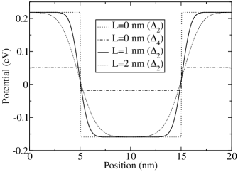
A 10 nm (100) -type QW between two 5 nm Si0.5Ge0.5 barriers is shown in fig. 1, with the in-plane lattice constant set to achieve strain balance. As increases, the bottom of the well narrows and the top widens. The effect on scattering in (100) - and -type and in (111) -type systems is discussed in depth in the following sections.
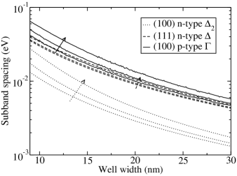
Interdiffusion increases the separation of low energy subbands as shown in Fig. 2. As scattering rates depend on subband separation, interdiffusion affects scattering in two possible ways:
-
1.
A direct effect due to the change in interface geometry.
-
2.
An indirect effect due to the change in subband spacing.
Throughout this section, we adjust the width of QWs to correct the interdiffusion effect on subband separation. The calculated change in scattering rates is therefore due only to the change in interface geometry. In section IV, the total effect is determined by varying interdiffusion without correcting the subband separations.
III.1 (100) -type single QW
In Si1-xGex alloys with %, the conduction band has six minima near the Brillouin zone edge in the directions.Paul (2004) The valleys are almost parabolic, and a single band effective mass approximation (EMA) accurately models electron confinement.Harrison (2005)
The valleys have ellipsoidal equipotential surfaces with their major axes along the cubic unit cell edge directions. Two separate effective masses are defined for electrons with wave vectors near the minima: the longitudinal mass, and the transverse mass, .Rieger and Vogl (1993) Quantum confinement in the direction in strained (100) systems yields four degenerate subbands with quantization effective mass, and two subbands with . As shown in fig. 1, the conduction band edge is at a relatively high energy and it can be assumed to have a negligible electron population. The following discussion therefore considers only scattering between subbands and omits -phonon emission processes.
A more precise double valley EMA models states with as a combination of basis states from the two valleys. In confined systems, the phase difference between reflected basis components splits the degeneracy of the subbands. We have previously shown however, that the splitting is quite small for QWs wider than 2–3 nm and it is therefore omitted in this work.Valavanis et al. (2007)
The width of a Si QW between a pair of Si0.5Ge0.5 barriers (as in fig. 1) was adjusted for =10 meV for a given diffusion length. Scattering rates were then calculated as a function of and are shown in fig. 3.
All mechanisms except alloy disorder scattering were found to be almost independent of diffusion length and their rates are only plotted for the abrupt interface system, for simplicity. For all diffusion lengths, Coulombic interactions and interface roughness rates were relatively large. As interdiffusion increases however, the alloy disorder rate increases very rapidly, from 5 s-1 for =0 nm to 1.1 s-1 for =2 nm. As described previously, this is due to alloy disorder scattering being permitted in the well region of diffuse structures, where the electron probability is large.
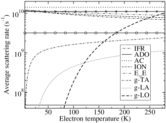
The electron temperature dependence of the average alloy disorder and intravalley acoustic phonon scattering rate is shown to be weak in fig. 3, as the scattering potentials depend neither on the initial wave vector nor explicitly on the electron temperature. The interface roughness scattering however depends on the initial wave vector and hence the average rate is affected by the temperature dependent distribution of electrons in the subband. The screening of the Coulombic interactions is also affected by electron temperature, explaining the gradual decrease in average rate. Finally, the intervalley phonon emissions are affected very strongly by electron temperature because the subband spacing is lower than for each of the permitted phonons.Dollfus (1997) The average scattering rate therefore depends on the number of electrons with sufficient initial kinetic energy to scatter into a state within the lower subband.
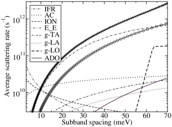
In pump–probe experiments, which are often used to determine scattering lifetimes, the carrier temperature, is elevated above the lattice temperature, and decays over time. We have previously shown however, that good agreement with experimental data is achievable by assuming 20 K.Califano et al. (2007) In fig. 4, we show the average intersubband scattering rate as a function of subband separation at 4 K, =24 K.
For =0 nm and subband spacing closer than 10 meV, ionized impurity and electron–electron scattering dominate, while at spacings between 10 meV and 55 meV, interface roughness and intravalley acoustic phonon scattering are fastest. As the subband spacing becomes comparable to the energy of the -LO phonons, the emission rate exceeds the intravalley acoustic phonon scattering rate. Alloy disorder scattering is again shown to increase significantly with interdiffusion and becomes dominant for subband spacing above 10 meV and =2 nm.
III.2 (111) -type single QW
Several important changes are introduced by moving to the (111) orientation. Electron confinement is now determined using an oblique cross-section of the ellipsoidal equipotential surface in -space, which is identical in all six valleys. The quantization effective mass isRahman et al. (2005)
| (14) |
compared with =0.916 for the valleys in (100) systems. The density-of-states effective mass isRahman et al. (2005)
| (15) |
compared with =0.19 for the valleys in (100) systems.
The uniaxial strain splitting exhibited in (100) is absent in (111) systems, while the hydrostatic strain induced shift in conduction band potential is given by
| (16) |
where are elastic constants, are deformation potentials, and is the in-plane strain as opposed to
| (17) |
for (100) systems.Smirnov and Kosina (2004) For a strain symmetrized 10 nm Si QW between two 5 nm Si0.5Ge0.5 barriers, the conduction band offset is around 150 meV, compared with around 380 meV for the offset in (100) as shown in fig. 1 As the valley degeneracy is not split, the population of subbands in each valley is equal and -phonon processes are no longer negligible. Fig. 5 shows the average intersubband scattering rates in a (111) -type Si QW between two 5 nm Si0.5Ge0.5 barriers with =24 K as a function of subband separation.
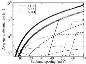
The Coulombic interactions and the intravalley- and -phonon interactions are almost unchanged compared with the (100) case. From eqn. 9, it can be deduced that the reduced conduction band offset reduces the interface roughness scattering rate in (111) systems slightly. More significantly, a larger well width is required to achieve an equivalent subband splitting and hence a smaller proportion of the wave functions extend over the interface region. The scattering matrix element is therefore smaller than in the (100) case. The alloy disorder scattering is also slightly increased by the change in density-of-states effective mass.
The zero-order -phonon emission processes become large at and in structures with abrupt interfaces represent the dominant mechanisms. -phonon interactions have four destination valleys and therefore dominate over -phonons, which have only a single destination.
III.3 (100) -type single QW
The band structure for hole transitions is highly nonparabolic and state contributions from the light hole (LH), heavy hole (HH), and spin split-off (SO) bands are all significant at nonzero in-plane wave vectors. The single band EMA is therefore inadequate and the 66 solution described previously,Ikonic et al. (2004) was used to account for the multiband effects.
As Si/SiGe forms type II heterointerfaces, the well and barrier compositions of the structure used for -type systems were reversed. The resulting HH band offset was 350 meV. The well width was adjusted to give a 10 meV separation between the two lowest HH states at . Fig. 6 shows the average intersubband scattering rates for the system as a function of hole temperature, .
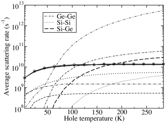
The results differ considerably from those of the -type systems considered previously. As increases, the hole distribution spreads over a larger range of in-plane wave vector and HH states acquire a larger LH contribution. This affects both the scattering matrix element and the effective density of states, resulting in an increase in all rates.
The carrier–carrier scattering rate depends on the overlap between initial and final states for a pair of carriers and is strongly dependent on the in-plane wave vector of the involved states and hence on hole distribution over . The dependence is therefore extremely strong and carrier carrier scattering dominates above =65 K in this system. Below this temperature, alloy disorder scattering is dominant.
In contrast with -type systems, alloy disorder scattering in -type systems is very weakly dependent on interdiffusion. This is because the magnitudes of wave functions are largest in the center of the QW, where the Ge fraction is barely affected by the interdiffusion.
IV Growth process tolerance
We have so far considered the effect of interdiffusion on intersubband transitions of known energies. Interdiffusion due to growth processes however changes the subband separation as well as the scattering rates. There are therefore important implications for fabrication of intersubband devices such as RTDs and QCLs. The following method uses both these effects to estimate the tolerance of a device design to undesired interdiffusion.
A (100) -type double QW system with two coupled Si wells of width 5 nm and 3 nm, separated by a 1 nm Si0.5Ge0.5 barrier provides a relatively simple example similar to that used in our previous pump–probe investigation of intersubband transition lifetimes in -type materials.Califano et al. (2007) The system was surrounded by a pair of 5 nm thick Si0.5Ge0.5 barriers as before. For simplicity, the symmetric approximation for interdiffusion was preserved and the temperatures were fixed at =4 K and =24 K. The scattering rates and subband separation are plotted in fig. 7.
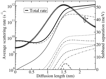
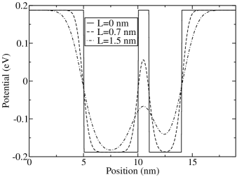
In the nominal structure, the layers are defined precisely, restricting alloy disorder scattering to the barrier regions. The separating barrier is thick enough for the coupling to be very weak between states. The subband separation of 17.5 meV is too low for phonon emission to be significant, although large enough (and the matrix element small enough) for Coulombic interactions to be negligible. The dominant rate is therefore interface roughness scattering, which is also slowed by the small overlap between states. As the interdiffusion increases, the device behavior varies and can be characterised by the following operating regimes, which are illustrated in fig. 8.
-
1.
Uncoupled wells ( nm): When interdiffusion is small, extra Ge in the wells increases alloy disorder scattering. The overlap of states is decreased as the bottom of the barrier becomes thicker. The other scattering rates therefore decrease slightly. Conversely, the bottoms of the wells narrow and subband spacing is increased.
-
2.
Weakly coupled wells ( nm): For moderate interdiffusion, the barrier potential is substantially reduced, while the subband spacing is increased further. As the second subband minimum approaches the barrier potential, the overlap between states increases rapidly. All scattering rates therefore begin to rise extremely rapidly.
-
3.
Single well ( nm): For large interdiffusion, the second subband energy exceeds the barrier potential and the character of the system changes from that of a double QW to a single QW with a small central perturbation. The perturbation diminishes as interdiffusion increases and the subband separation decreases towards the value for a wide, single well. The effect on scattering is slightly more complex than the previous regimes.
The first-order electron–phonon rates remain almost constant as the effect of the increased overlap is countered by the decrease in subband separation. The -LO phonon emission however, decreases sharply due to its high frequency and zero-order character. Coulombic interactions continue to increase as the overlap between states increases and the subband separation decreases. Interface roughness scattering slows as the barrier potential diminishes and alloy disorder scattering continues to increase as the Ge content in the single well rises.
The total rate in fig. 7 remains almost constant at diffusion lengths below 1 nm, although the subband spacing varies considerably above 0.25 nm. A multiple QW device such as a QCL might therefore operate successfully with 1 nm interdiffusion if changes in transition energy are acceptable. Above this tolerance however, there are catastrophic changes in the device and both transition energies and lifetimes will be severely affected. This method may readily be applied to a wide variety of intersubband device designs as an estimator of robustness.
V Conclusion
We have simulated annealed interfaces to model real systems more accurately than the rectangular well approximation. The study of carrier dynamics has thus been extended to systems with diffuse interfaces (either by design or via the growth process). Intersubband scattering rates have been investigated as functions of subband separation and electron temperature in (100) -type and (100) and (111) -type diffuse QWs.
We have shown that for any given subband separation and electron temperature, the alloy disorder scattering increases rapidly with diffusion length in -type systems as Ge content in the well region increases. The alloy disorder scattering is a relatively minor effect in systems with abrupt interfaces, while in diffuse systems, it can become the dominant mechanism. In -type systems however, the effect is negligible as the Ge content in the center of the well remains large.
In the case of Ge interdiffusion introduced during growth, this implies that very simple -type system designs may be adjusted to preserve subband separations and carrier dynamic behavior if the achievable diffusion length is known. In -type systems however, the carrier dynamics may be strongly affected even when the design is adjusted to preserve subband separations.
The robustness of an example double (100) -type QW design was examined by considering the combined effect of Ge interdiffusion on both the subband separation and scattering rates. It was shown that a tolerance of 0.25 nm preserved the subband separation, while a less restrictive tolerance of 1 nm preserved the scattering rates.
As group IV heterostructure epitaxy is less developed than that of III–V systems, we propose that future designs of complex devices such as QCLs in the Si/SiGe materials system should be tested for their robustness using this method before attempting growth.
Acknowledgements.
This work is supported by EPSRC Doctoral Training Allowance funding. The authors are grateful to Marco Califano and Leon Lever, University of Leeds for useful discussions.References
- Pavesi et al. (2003) L. Pavesi, S. Gaponenko, and L. D. Negro, eds., Towards the First Silicon Laser (NATO Science Series II: Mathematics, Physics and Chemistry — Vol. 93) (Kluwer Academic Publishers, Dordrecht, 2003).
- Liu et al. (1988) H. C. Liu, D. Landheer, M. Buchanan, and D. C. Houghton, Appl. Phys. Lett. 52, 1809 (1988).
- Dehlinger et al. (2000) G. Dehlinger, L. Diehl, U. Gennser, H. Sigg, J. Faist, K. Ensslin, D. Grutzmacher, and E. Muller, Science 290, 2277 (2000).
- Bates et al. (2003) R. Bates, S. Lynch, D. Paul, Z. Ikonić, R. Kelsall, P. Harrison, S. Liew, D. Norris, A. Cullis, W. Tribe, et al., Appl. Phys. Lett. 83, 4092 (2003).
- Driscoll and Paiella (2006) K. Driscoll and R. Paiella, Appl. Phys. Lett. 89, 191110 (2006).
- Han and Yu (2007) G. Han and J. Yu, Semicond. Sci. Tech. 22, 769 (2007).
- Ikonic et al. (2004) Z. Ikonic, P. Harrison, and R. W. Kelsall, J. Appl. Phys. 96, 6803 (2004).
- Zhang et al. (2006) J. Zhang, S. Turner, S. Chiam, R. Liu, E. Tok, A. Wee, A. Huan, I. Kelly, and C. Mulcahy, Surf. Sci. 600, 2288 (2006).
- Li et al. (1996) E. H. Li, B. L. Weiss, and K.-S. Chan, IEEE J. Quantum. Electron. 32, 1399 (1996).
- Prange and Nee (1968) R. E. Prange and T.-W. Nee, Phys. Rev. 168, 779 (1968).
- Penner et al. (1998) U. Penner, H. Rücker, and I. N. Yassievich, Semicond. Sci. Tech. 13, 709 (1998).
- Sakaki et al. (1987) H. Sakaki, T. Noda, K. Hirakawa, M. Tanaka, and T. Matsusue, Appl. Phys. Lett. 51, 1934 (1987).
- Tsujino et al. (2005) S. Tsujino, A. Borak, E. Müller, M. Scheinert, C. V. Falub, H. Sigg, D. Grützmacher, M. Giovannini, and J. Faist, Appl. Phys. Lett. 86, 062113 (2005).
- Ando et al. (1982) T. Ando, A. B. Fowler, and F. Stern, Rev. Mod. Phys. 54, 437 (1982).
- Unuma et al. (2003) T. Unuma, M. Yoshita, T. Noda, H. Sakaki, and H. Akiyama, J. Appl. Phys. 93, 1586 (2003).
- Califano et al. (2007) M. Califano, N. Q. Vinh, P. J. Phillips, Z. Ikonic, R. W. Kelsall, P. Harrison, C. R. Pidgeon, B. N. Murdin, D. J. Paul, P. Townsend, et al., Phys. Rev. B 75, 045338 (2007).
- Gradshteyn and Ryzhik (2000) I. Gradshteyn and I. Ryzhik, Table of Integrals, Series, and Products (Academic Press, San Diego, 2000), sixth ed.
- Huan and Hai (2007) T. D. Huan and N. P. Hai, Phys. Status Solidi B 244, 2100 (2007).
- Quang et al. (2007) D. N. Quang, N. H. Tung, D. T. Hien, and H. A. Huy, Phys. Rev. B 75, 073305 (2007).
- Murphy-Armando and Fahy (2006) F. Murphy-Armando and S. Fahy, Phys. Rev. Lett. 97, 096606 (2006).
- Ikonić et al. (2001) Z. Ikonić, P. Harrison, and R. W. Kelsall, Phys. Rev. B 64, 245311 (2001).
- Canali et al. (1975) C. Canali, C. Jacoboni, F. Nava, G. Ottaviani, and A. Alberigi-Quaranta, Phys. Rev. B 12, 2265 (1975).
- Monsef et al. (2002) F. Monsef, P. Dollfus, S. Galdin, and A. Bournel, Phys. Rev. B 65, 212304 (2002).
- Davies (1998) J. H. Davies, The Physics of Low-Dimensional Semiconductors: An Introduction (Cambridge University Press, Cambridge, 1998).
- Smet et al. (1996) J. H. Smet, C. G. Fonstad, and Q. Hu, J. Appl. Phys. 79, 9305 (1996).
- Jovanovic et al. (2006) V. D. Jovanovic, S. Hofling, D. Indjin, N. Vukmirovic, Z. Ikonic, P. Harrison, J. P. Reithmaier, and A. Forchel, J. Appl. Phys. 99, 103106 (2006).
- Paul (2004) D. J. Paul, Semicond. Sci. Tech. 19, R75 (2004).
- Harrison (2005) P. Harrison, Quantum Wells, Wires and Dots (Wiley, Chichester, 2005), 2nd ed.
- Rieger and Vogl (1993) M. M. Rieger and P. Vogl, Phys. Rev. B 48, 14276 (1993).
- Valavanis et al. (2007) A. Valavanis, Z. Ikonić, and R. W. Kelsall, Phys. Rev. B 75, 205332 (2007).
- Dollfus (1997) P. Dollfus, J. Appl. Phys. 82, 3911 (1997).
- Rahman et al. (2005) A. Rahman, M. S. Lundstrom, and A. W. Ghosh, J. Appl. Phys. 97, 053702 (2005).
- Smirnov and Kosina (2004) S. Smirnov and H. Kosina, Solid State Electron. 48, 1325 (2004).