Nanoscale polarization switching mechanisms in multiferroic BiFeO3 thin films
Abstract
Ferroelectric switching in BiFeO3 multiferroic thin films with intrinsic “stripe-like” and “bubble-like” polydomain configurations was studied by piezoresponse force microscopy. Using the local electric field applied by a scanning probe microscope tip, we observe reversal of both out-of-plane and in-plane components of the polarization, with the final domain state depending on the tip sweeping direction. In “bubble-like” samples, complete control of the polarization is achieved, with in-plane polarization change mediated and stabilized by out-of-plane polarization reversal. In “stripe-like” samples the intrinsic domain structure influences polarization switching and in-plane reversal may occur without out-of-plane change. The observed switching behaviour can be well correlated with the radial and vertical components of the highly inhomogeneous electric field applied by the tip.
The co-existence of ferroelectric and antiferromagnetic ordering at room temperature in BiFeO3 (BFO) has made this material the focus of intense research, both aimed at understanding its fundamental properties, and at exploiting them in multifunctional device applications (see for instance Catalan09 ; Bibes08 and references therein). Magnetoelectric coupling between the orders, allowing the rotation of the antiferromagnetic ordering via the application of electric field, has been demonstrated in both thin films Zhao06 and bulk single crystals Lebeugle08 , although the bulk magnetoelectric coefficient has been determined to be extremely small Popov93 . The magnetoelectric effect was subsequently used to control the exchange bias BeaEB and to electrically control the magnetization of metallic layers magnetically coupled to BFO Chu08 . In spite of these application-oriented advances, open questions remain about the mechanism behind the observed magnetoelectric coupling, and especially about its effects at the nanoscale, the proposed regime for future device implementation. Extensive quantitative studies have been rendered challenging in part by the complex ferroelectric structure of BFO, with eight equivalent variants of polarization giving rise to nanoscale domains separated by three different types of domain walls (71, 109 and 180∘ Zhao06 ), some of which themselves present additional functionalities, such as conduction Seidel09 , absent from the parent material. Moreover, in epitaxial thin films, different intrinsic ferroelectric domain configurations can be observed, in which some of the eight polarization variants appear to be suppressed depending on the growth conditions, the bottom electrode, the substrate and substrate miscut, ranging from monodomain, to “stripe-like” and “mosaic-like” polydomain Chu07 and to “bubble-like” polydomain Catalan08 . For fundamental insight into the mechanisms behind magnetoelectric coupling in BFO thin films, and for their use in technological applications, nanoscale control of the ferroelectric domain structure and understanding of local ferroelectric switching mechanisms is thus of key importance. Macroscopic polarization switching has been studied using parallel electrodes to apply homogenous out-of-plane Gruverman05 or in-plane electric fields Shafer07 , albeit separately. To be able to both switch the polarization and to measure all its components, it is also possible to use liquid electrodes Rodriguez07 . Another option to study full polarization switching and to avoid leakage is to use the metallic tip of an atomic force microscope as an electrode Zavaliche05APL . In this configuration, a local, intense, but highly inhomogeneous field is generated with both a vertical component allowing out-of-plane switching, and a horizontal component with approximately radial symmetry due to the tip shape. After switching, piezoresponse force microscopy (PFM) can be used to fully characterize the polarization, allowing access to nanoscale switching mechanisms.
In this letter, we present a detailed PFM study of the polarization switching mechanisms that occur in BFO thin films under a biased atomic force microscope tip. In the case of “bubble-like” BFO films, we observe switching of the in-plane polarization only when associated with out-of-plane polarization reversal. In the case of “stripe-like” BFO films, the in-plane component of the polarization may switch independently. In both cases the radial electric field of the tip, as well as its sweep direction, strongly influence the polarization switching. In “bubble-like” samples, these mechanisms may allow a complete control of both components of the polarization without in-plane electrodes.
For these studies, we used 50–70 nm thick BFO films deposited on (001)-oriented SrTiO3 (STO) substrates by pulsed laser deposition BeaAPL2 (giving “bubble-like” films) and rf magnetron sputtering (“stripe-like”), on top of 25-35 nm thick SrRuO3, used as a bottom electrode. The high crystalline quality of the samples has been confirmed by X-ray diffraction (see Beaphilmag for the 70nm “bubble-like” sample, similar results being obtained for the 50 nm “stripe-like” film). The rms roughnesses of the presented films are 2nm in the “bubble-like’ case and 0.4nm in the “stripe-like” case. Ferroelectric domain writing and PFM measurements were performed using a Nanoscope V Dimension (20kHz, 3-4V ac, NCS18/Cr-Au from masch). In these films, we wrote domain structures by applying a voltage (equivalent to a nominal field of around 170MV/m in both presented samples) to the conductive tip while sweeping it in the desired pattern. Because the polarization in BFO lies close to the 111 directions, and thus presents both out-of-plane and in-plane components in these (001) oriented films, the written regions are then measured by both vertical and lateral PFM (VPFM and LPFM, respectively). When discussing PFM images, we mean PFM phase image, unless otherwise stated.
We first studied “bubble-like” polydomain BFO films presenting all eight variants of the polarization in the as-grown regions, in which VPFM and LPFM show an intrinsic domain structure somewhat correlated with surface morphology (Catalan08 and Fig. 1e). On such film, we prepolarized wide horizontal lines with alternating positive and negative voltage on a 3x3m2 area.
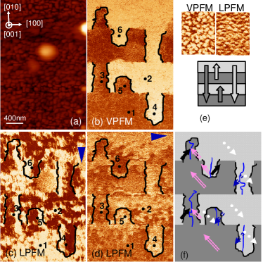
Subsequently, narrower vertical lines were written with positive or negative voltage while sweeping the tip either along [010] or [00] (Fig. 1e). The domains written with negative voltage (“up” polarization, regions 1, 3, 5) show a dark VPFM contrast (Fig. 1b), while the positive-voltage-written domains are bright (regions 2, 4, 6). As expected, when a vertical line written with negative (resp. positive) voltage crosses a region prepolarized with positive (resp. negative) voltage, the out-of-plane polarization component is reversed, while when it crosses a negatively (resp. positively) prepolarized region no change in the VPFM contrast is observed.
In the LPFM images (Fig. 1c and d), we observe that the in-plane configuration of the polarization has also been clearly modified as compared to the as-grown film (Fig. 1e). In negatively prepolarized rectangles (region 1), the LPFM signal of Fig. 1c presents a bright contrast indicating an in-plane component along [00], while for the positively prepolarized rectangles (region 2), a predominant dark contrast is obtained with a certain amount of bright regions, giving a predominant component along [100]. In these rectangles, the LPFM signal along the [010] direction (Fig. 1d) shows a bright contrast after a positive applied voltage (region 2) and a dark contrast after a negative applied voltage (region 1). In the negatively polarized rectangles, we thus obtain a monodomain configuration 111The as-grown configuration of this film being preferentially “down” (Fig. 1e), in the positively prepolarized rectangles, the in-plane configuration was not fully controlled due to the need for an accompanying out-of-plane switching.
During the vertical tip sweeps, the in-plane component of the polarization was similarly modified, but only in the specific regions in which the out-of-plane polarization component was also reversed during writing (outlined in black in Fig. 1b-d). In these regions, for the cantilever oriented along the vertical lines (Fig. 1c), a characteristic pattern is observed: a dark LPFM contrast on the right of the cantilever and a bright one on its left for the negative-voltage-written lines (regions 3, 5) while the reverse is true for lines written with a positive voltage (regions 4, 6). This pattern correlates with the horizontal component of the electric field perpendicular to the cantilever axis. The in-plane polarization switching is thus assisted by the out-of-plane polarization switching in this range of fields and reproduces the horizontal electric field distribution.
Imaging the in-plane domain structure of the vertical lines with the cantilever rotated by 90∘ (Fig. 1d), we again observe that the only regions where the in-plane component of the polarization has been modified are the regions where the out-of-plane component of the polarization has also been reversed (again, outlined in black). In these measurements, however, the LPFM contrast not only depends on the polarity of the applied voltage but also varies as a function of the tip sweeping direction during writing. For a negative voltage, where the tip moved along [00] (region 3), a dark contrast is observed whereas where the tip moved along [010], the contrast is bright (region 5). For a positive voltage, the opposite is observed: where the tip moved along [00], the contrast is bright (region 4) and when the tip moved along [010], the contrast is dark (region 6). In Fig. 1f, we have summarized both out-of-plane (bright or light gray) and in-plane polarization orientations (arrows) in the written regions.
We then carried out similar measurement on “stripe-like” films, as shown in Fig. 2.
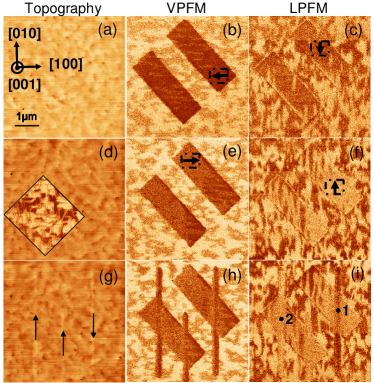
In this case, the as-grown film presents only the four “down” polarization components (ie. bright contrast in VPFM images of Fig. 2b, e, h), with stripe-like features as observed in the LPFM image in inset of Fig. 2d. We note that the VPFM contrast is not homogeneously bright in the as-grown region, but presents clear structure, with faintly darker regions corresponding to a noisier phase and to a decrease in VPFM amplitude (data not shown). This may be attributed to a buckling of the cantilever in response to an in-plane piezoresponse along the cantilever axis Peter06 ; Shafer07 . Contrary to the “bubble-like” film 222In the “bubble-like” film, the roughness was higher, probably making the buckling signal more difficult to access., in the case of a “stripe-like” film, only one VPFM image and one LPFM image are thus necessary to reconstruct the total polarization configuration.
On this sample, we have written two sets of two rectangles with negative voltage by sweeping the tip with its slow scan axis along either [0] (Fig. 2a-c) or [110] (Fig. 2d-f). In both cases, the out-of-plane polarization has been switched in these regions, as checked by a measurement made with the cantilever rotated by 90∘ to distinguish deflection from buckling contributions (not shown).
Considering the in-plane signals, we see that in the LPFM images (Fig. 2c and f) the written regions are not fully monodomain, but rather present a predominant contrast with a few stripes corresponding to the opposite in-plane polarization orientation. Similarly, in these regions, the VPFM signal is not homogeneous due to the buckling contribution, and is composed in Fig. 2b (resp. Fig. 2e) of a predominant dark (resp. faintly brighter) contrast with a few stripes presenting the opposite contrast, ie. faintly brighter (resp. dark). Comparing the sets of measurements of Fig. 2b-c and e-f, we clearly see that these predominant contrasts are opposite, thus revealing opposite in-plane component of the polarization both along [100] (see boxes and arrows in Fig. 2b and e) and [010] directions (see boxes and arrows in Fig. 2c and f). To summarize, the predominant resulting in-plane configuration is reversed when the slow scan axis during writing was along [110] or [0], in agreement with the conclusions obtained for the “bubble-like” film.
As for the “bubble-like” film, we then wrote vertical lines with negative tip voltage, sweeping along the directions indicated in Fig. 2g, and measured the resulting domain pattern (Fig. 2g-i). Strikingly, and unlike what we observe in the “bubble-like” film, the in-plane component of the polarization has been modified even when the out-of-plane polarization was not switched. This can be seen in particular in Fig. 2i, where a dark (region 1) or bright (region 2) line appears in the previously written rectangle. Also, the in-plane contrast of the written lines along [100] (from buckling signal in Fig. 2h) is similar to that obtained for the negative-voltage-written lines in the “bubble-like” film, ie. directed towards the tip. Along the [010] direction (from LPFM in Fig. 2i), the contrast depends on the sweeping direction: a bright contrast is obtained for the tip sweeping along [010] (region 2) and a dark contrast for the [00] direction (region 1).
To understand the observed switching of the in-plane polarization components, we need to consider the electric field generated by the AFM tip.
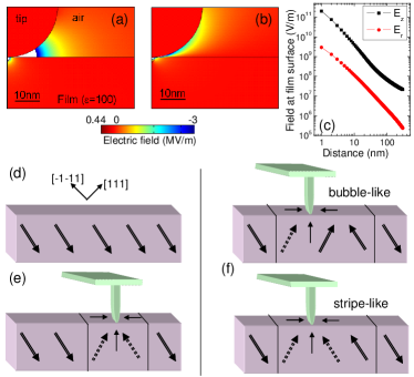
Using COMSOL Multiphysics, we modeled a tip with a realistic shape in contact with a 200nm-thick insulating film presenting a dielectric constant of 100 on top of a metal electrode. As expected, this electric field is highly inhomogeneous with both a vertical component Ez (Fig. 3a) and a radially-symmetric horizontal component Er (Fig. 3b). On the film surface, as plotted in Fig. 3c, both vertical and horizontal components of the electric field decrease as the inverse of the distance from the tip. However their magnitudes are very different, the horizontal field being two orders of magnitude smaller than the vertical field. In fact, simply considering the electric field profile, switching the in-plane polarization using the AFM tip would appear to be significantly more difficult than switching the out-of-plane polarization.
Coherently with this picture, we previously observed that in (111)-oriented films presenting two purely out-of-plane polarization variants, the application of an electric field through the tip results only in the purely out-of-plane variant BeaAPL111 , in agreement with other experiments Seidel09 . In that case where a purely out-of-plane polarization is possible, the in-plane field is thus too small to rotate the polarization in a strongly in-plane direction, and a purely out-of-plane polarization is stabilized during switching. On the other hand, in the case of (001)-oriented films, all variants of the polarization have equivalent in-plane components. The small in-plane field of the AFM tip thus renders these variants inequivalent, and could lead to stabilization of a modified in-plane polarization component.
To summarize these observations, we propose a switching mechanism for the polarization in a monodomain BFO thin film under a biased tip, as presented in Fig. 3d-f. These figures give a schematic representation of a negatively polarized tip sweeping towards the left. First, for both types of samples, the polarization initially oriented along [11] (Fig. 3d) is switched underneath the tip: on the left of the tip, the polarization is now oriented along [111] while on its right, it is oriented along [1] (Fig. 3e), following the vertical and horizontal local electric field. Then, in a “bubble-like” film, as the tip sweeps leftwards (Fig. 3f, upper part), switching will continue only on the left of the cantilever: the region on its right being already “up”, neither the out-of-plane nor the in-plane component of the polarization will change, in agreement with experimental observations. In the switching region, the horizontal field of the tip is directed right, and the polarization will now point in the [111] direction. In the end, the in-plane component of the polarization will thus present a thin stripe with polarization oriented along [1] in the initial switching region and then along [111] for the rest of the area swept by the tip. For a “stripe-like” film, when the tip sweeps leftwards (Fig. 3f, lower part), both in-plane and out-of-plane components of the polarization may be switched: the region on the right of the tip in the [1] direction, while on its left in the [111] direction. Obviously, in both types of samples, if the tip sweep direction or voltage are changed, the final in-plane component of the polarization will be affected. In this representation of switching, we therefore expect the final in-plane component of the polarization to be oppositely directed for the same writing pattern for the two different types of film. This expectation is borne out experimentally: for negative voltage, in the “bubble-like” films, the predominant in-plane component of the polarization is opposite to the sweeping direction (see regions 1, 3, 5 of Fig. 1) while in the “stripe-like” films, it is along the sweeping direction (see boxes and arrows in Fig. 2).
To conclude, we have shown the possibility of a full control over the 111-oriented polarization direction of “bubble-like” (001)-BFO thin films by using a biased sweeping AFM tip. In “stripe-like” films, an incomplete in-plane switching and non-monodomain regions are obtained, depending on pre-existing domain structure. In these latter films, the final stable domain structure imaged by PFM could in fact be the result of a more complex switching path exploring the eight variant configurations BalkePFM09 . The switching mechanism in the two types of films appears to be different, with in-plane switching occurring more easily and independently of out-of-plane switching in the “stripe-like” films. This suggests that the coercive fields for in-plane and out-of-plane components of the polarization could be different in the two cases, which could be linked to surface morphology, type of domain walls or pinning defects. Different behavior depending on the as-grown domain and domain wall configuration of the BFO thin films was already observed for instance in exchange biased ferromagnetic/BFO bilayers MartinEB08 . Finally, the polarization control in “bubble-like” films demonstrated in this work, allowing desired domains and domain walls in BFO thin films to be defined using small in-plane fields, can be very useful in future devices and for fundamental studies of magnetoelectric coupling mechanisms at the nanoscale.
Acknowledgements.
The authors thank J.-M. Triscone, K. Bouzehouane and S. Fusil for helpful discussions. Technical support by M. Lopes and E. Jacquet is acknowledged. This work was supported by the Swiss National Science Foundation through the NCCR MaNEP and Division II, by the European Commission STREP project MaCoMuFi. H.B. is supported by a Bourse d’Excellence from the University of Geneva.References
- (1) G. Catalan and J.F. Scott, Adv. Mater., 21, 2463 (2009).
- (2) M. Bibes and B. Barthélémy, Nat. Mater., 7 (2008).
- (3) T. Zhao, A. Scholl, F. Zavaliche, K. Lee, M. Barry, A. Doran, M.P. Cruz, Y.H. Chu, C. Ederer, N.A. Spaldin, R.R. Das, D.M. Kim, S.H. Baek, C.B. Eom, and R. Ramesh, Nat. Mater., 5, 823 (2006).
- (4) D. Lebeugle, D. Colson, A. Forget, M. Viret, A.M. Bataille, and A. Gukasov, Phys. Rev. Lett., 100, 227602 (2008).
- (5) Yu.F. Popov, A.K. Zvezdin, G.P. Vorob’ev, A.M. Kadomtseva, V.A. Murashev, and D.N. Rakov, JETP Letters, 57(1), 69 (1993).
- (6) H. Béa, M. Bibes, F. Ott, B. Dupé, X.-H. Zhu, S. Petit, S. Fusil, C. Deranlot, K. Bouzehouane, and A. Barthélémy, Phys. Rev. Lett., 100, 017204 (2008).
- (7) Y.-H. Chu, L.M. Martin, M. B. Holcomb, M. Gajek, S.-J. Han, Q. He, N. Balke, C.H. Yang, D. Lee, W. Hu, Q. Zhan, P.-L. Yang, A. Fraile-Rodríguez, A. Scholl, S.X. Wang, and R. Ramesh, Nat. Mater., 7, 478 (2008).
- (8) J. Seidel, L. W. Martin, Q. He, Q. Zhan, Y.-H. Chu, A. Rother, M. E. Hawkridge, P. Maksymovych, P. Yu, M. Gajek, N. Balke, S. V. Kalinin, S. Gemming, F. Wang, G. Catalan, J. F. Scott, N. A. Spaldin, J. Orenstein, and R. Ramesh, Nat. Mater., 8, 229 (2009).
- (9) Y.-H. Chu, M. P. Cruz, C.-H. Yang, L. W. Martin, P.-L. Yang, J.-X. Zhang, K. Lee, P. Yu, L.-Q. Chen, and R. Ramesh, Adv. Mat., 19, 2662 (2007).
- (10) A. Gruverman, B.J. Rodriguez, C. Dehoff, J.D. Waldrep, A.I. Kingon, R.J. Nemanich, and J.S. Cross, Appl. Phys. Lett., 87, 082902 (2005).
- (11) P. Shafer, F. Zavaliche, Y.-H. Chu, P.-L. Yang, M. P. Cruz, and R. Ramesh, Appl. Phys. Lett., 90, 202909 (2007).
- (12) B. J. Rodriguez, S. Jesse, A. P. Baddorf, S. H. Kim, and S.V. Kalinin, Phys. Rev. Lett., 98, 247603 (2007).
- (13) F. Zavaliche, R.R. Das, D.M. Kim, C.B. Eom, S.Y. Yang, P. Shafer, and R. Ramesh, Appl. Phys. Lett., 87, 182912 (2005).
- (14) H. Béa, M. Bibes, M. Sirena, G. Herranz, K. Bouzehouane, E. Jacquet, S. Fusil, P. Paruch, M. Dawber, J.-P. Contour, and A. Barthélémy, Appl. Phys. Lett., 88, 06252 (2006).
- (15) H. Béa, M. Bibes, S. Petit, J. Kreisel, and A. Barthélémy, Philos. Mag. Lett., 87(3-4), 165 (2007).
- (16) G. Catalan, H. Béa, S. Fusil, M. Bibes, P. Paruch, A. Barthélémy, and J.F. Scott, Phys. Rev. Lett., 100, 027602 (2008).
- (17) F. Peter, A. Rdiger, and R. Waser, Rev. Sci. Instr., 77, 036103 (2006).
- (18) H. Béa, M. Bibes, X.-H. Zhu, S. Fusil, K. Bouzehouane, S. Petit, J. Kreisel, and A. Barthélémy, Appl. Phys. Lett., 93, 072901 (2008).
- (19) N. Balke, ”Deterministic control of polarization switching in multiferroic materials”, International Symposium PFM - 2009 Aveiro, Portugal (2009).
- (20) L.W. Martin, Y.-H. Chu, M.B. Holcomb, M. Huijben, P. Yu, S.-J. Han, D. Lee, S.X. Wang, and R. Ramesh, Nanolett., 8, 2050 (2008).