AC transport in graphene-based Fabry-Pérot devices
Abstract
We report on a theoretical study of the effects of time-dependent fields on electronic transport through graphene nanoribbon devices. The Fabry-Pérot interference pattern is modified by an ac gating in a way that depends strongly on the shape of the graphene edges. While for armchair edges the patterns are found to be regular and can be controlled very efficiently by tuning the ac field, samples with zigzag edges exhibit a much more complex interference pattern due to their peculiar electronic structure. These studies highlight the main role played by geometric details of graphene nanoribbons within the coherent transport regime. We also extend our analysis to noise power response, identifying under which conditions it is possible to minimize the current fluctuations as well as exploring scaling properties of noise with length and width of the systems.
pacs:
73.23.-b, 72.10.-d, 73.63.-b, 05.60.GgTime-dependent fields (such as a time-dependent gate voltage or laser) Platero2004 ; Kohler2005 ; Buettiker2000 allow for novel electronic transport phenomena beyond the realm of static fields. Prominent examples include quantum charge pumping Thouless1983 ; Altshuler1999 ; Switkes1999 ; Prada2009 and coherent destruction of tunneling Grossmann1991 . Crucial to these phenomena is the interplay between quantum interference and photon-assisted processes. An equally relevant role is played by the electronic structure of the material constituting the device.

Carbon based materials such as carbon nanotubes (CNTs) Charlier2007 , graphene Novoselov1999 and graphene nanoribbons Han2007 constitute a promising test ground for these studies due to their outstanding electrical propertiesCharlier2007 ; CastroNeto2009 which are at the center of many promising applications as sensors Kibis2007 , switches delValle2007 and interconnects Coiffic2007 . Here, our focus is in graphene nanoribbons, where, thanks to low resistance contacts, Fabry-Pérot (FP) quantum interference patterns were observed miao2007 . Such low temperature experiments expand previous studies showing similar phenomena for CNT devices Liang2001 . For this last case, besides the conductance properties, the current noise Blanter2000 has also been experimentally probed in the FP regime Wu2007 ; Herrmann2007 ; YoungKim2007 .
Our contribution complements other recent studies of driven transport in nanotubes Orellana2007 ; Oroszlany2009 , the effects of electromagnetic irradiation in both single layer Trauzettel2007 ; Syzranov2008 ; Rodriguez08 ; Shafranjuk2008 ; Oka2009 ; Rivera2009 ; Danneau2008 and bilayer graphene Shafranjuk2009 ; Wright2009 ; Abergel2009 , and quantum pumping in graphene Prada2009 . In contrast to 2d graphene, in graphene nanoribbons the edges play a decisive role as will be shown later. On the other hand, studies focusing on AC response of graphene materials usually resort to a Dirac equation and a linear band approximation, something that does not always hold for graphene nanoribbons. Indeed, whenever higher energy bands play an important role or when the influence of the edges, and/or disorder Cresti2008 ; Long2008 or doping Biel2009 influences the electronic structure, these approximations need to be removed.
In this paper we study the effects of ac gating on the conductance and noise of graphene nanoribbons in the FP regime. In particular, we show that the interplay between the ac field parameters (field intensity and frequency) and the typical energy scales of the ribbon/nanotube (such as level spacing- and position of van Hove singularities) can lead to strong modifications on the conductance and current noise. In contrast to CNTs Torres2009 (where the results were independent on the helicity), the shape of the edges of the graphene nanoribbons turns out to have a dramatic effect on the interference pattern. Here, two paradigmatic situations are considered: armchair edges (AGNR) and zizag edges (ZGNR), see scheme in Fig.1. For the former, the situation coincides with the one of CNTs: the interference patterns observed in static conditions can be either suppressed, exhibit a revival or show an ac-intensity independent behavior by tuning the field intensity and frequency, while the current noise vanishes whenever the frequency is commensurate with twice the mean level spacing (quantum wagon-wheel or stroboscopic effect). We also extend this investigation to zigzag-edge nanoribbons and we demonstrate that the topological shape of the edges strongly determines the behavior of the patterns. In the following we briefly present the theoretical framework used for our calculations, then our results and finally our conclusions.
I Methodology
In this section the general formalism used in our calculations is outlined. The Hamiltonian of our system is written as:
| (1) |
where the sublabels L, R and C represent the contributions from the isolated left, right and central parts, respectively, and T corresponds to the connection between the leads and the central scattering region. In the standard tight-binding real space basis each one of those terms can be written in terms of quantum operators as
| (2) |
where () is the electron creation (annihilation) operator at site and or . The elements and are the on-site energy and the nearest neighbor hopping term, respectively. The parameter eV corresponds to the typical carbon-carbon hopping element and it is chosen to be our energy unit. The time dependence is introduced by adding a time dependent component to the on-site energies of atoms located in the scattering region to simulate the presence of an AC gate plate. Thus, where the AC parameters are , the amplitude of the potential and , the frequency. The bias voltage is assumed to be equally distributed among the two contacts as required to quasi-ballistic transport and a gate voltage is applied to the central region () which shifts the energy levels.
The contact term is given by
| (3) |
and we simulate quasi-transparent coupling between the electrodes and the sample Krompiewski2002 using . Our non-interacting model requires screening by a metallic substrate or by the surrounding gate that lessens electron-electron interactions. When these interactions come into play effects beyond our present scope may emerge Guigou2007 ; BinheWu2009 .
Additional ingredients beyond the stationary theory have to be considered for the treatment of quantum driven systems. A general framework valid for noninteracting systems is the use of a Floquet approach Camalet2003 ; Kohler2005 , which can also be combined with Green’s function formalism FoaTorres2005 . Within this formalism, the DC component of the current can be written as Kohler2005
| (4) |
being the electronic transmission of carriers coming from right to left leads which might absorb or emit photons depending if or , respectively. This means that an electron with initial energy has a certain probability of being scattered to a final energy state of .
Assuming an homogeneous driving as well as a weak energy dependence of the self-energy due to the electrodes, both spatial and time dependencies of the Floquet states can be factorized and the transport properties can be calculated within simple Tien-Gordon theoryTien1963 . Then, the average current over time can be computed as
| (5) |
where is the transmission in the absence of the driving field. For the case of a harmonic AC field, the coefficients correspond to Bessel functions of the first kind, . In turns, the transmission function is written in terms of Green functions (GF) according to the standard trace formula. On the other hand, the noise power (zero frequency component of the current-current correlation function) can be derived for such homogenous driven systemKohler2005 ,
| (6) | ||||
where are the retarded Green function between layers and . The elements are given in terms of the self-energy of the corresponding electrode [ with ] being the retarded surface Green function of the lead .
More general situations where the time-dependent potential is space-dependent could be solved by using the full Floquet theory Moskalets2002 ; Camalet2003 , methods resorting to equations of motion Agarwal2007 ; Jin2008 , density functional theory Kurth2005 or the Keldysh formalism Pastawski1992 ; Jauho1994 ; Arrachea2005b . However, even for homogeneous gating, the approach described above can be heavily demanding in terms of computational cost depending on the size of the system (matrices of dimension where is the number of atoms along one layer of the ribbon need to be invert at each step of the decimation procedure). While this is indeed the case for the ZGNRs, for AGNRs the problem can be sensibly reduced thanks to a change of basis transformation which is introduced in detail in Appendix A.
Based on the tools introduced before we are able to investigate how the quantum transport properties of GNRs are affected by the AC field. These results are presented in the next session and help to sketch a panorama of of the response of both armchair and zigzag nanoribbons to such perturbation. Our numerical analysis and interpretations are also supported by analytical expressions detailed on the appendix.
II
Results
II.1 Direct Current conditions
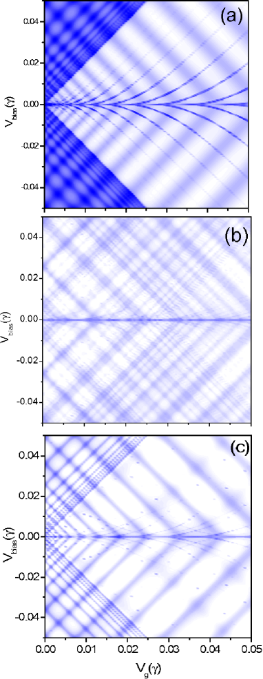
As previously mentioned, FP patterns can be generated in electron waveguide systems with the aid of time independent gate and bias voltages. The quasi-transparent contacts between the leads and the conductor confines the electronic wave functions as in light resonant cavity in which coherent propagation modes can interfere destructively or constructively generating an interference pattern. In this sense, an oscillatory behavior of the electronic transmission is observed while tuning the external voltages and the shape of this pattern is strictly dependent on the electronic structure of the system. Depending on the atomic details of their edges, graphene nanoribbons can reveal remarkable differences on their band structures and therefore generate distinct patterns as can be seen directly from Fig. 4. On the upper panel, we present the FP pattern for an AGNR system and underneath it is shown the picture for a ZGNR.
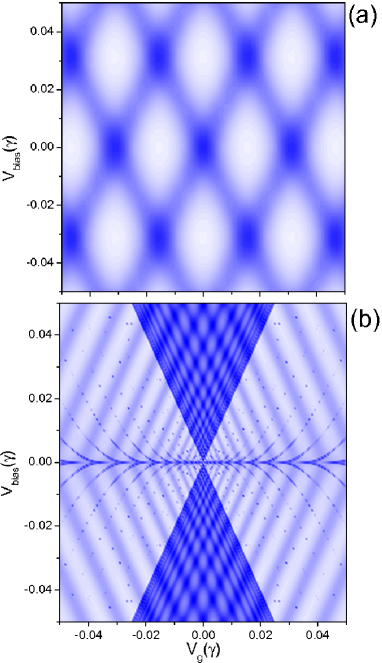
Firstly, we focus on Fig 4(a) obtained for an AGNR. The low energy linear dispersion of AGNRs guarantees a regular energy spacing level scale, , when the system is brought to near-perfect ohmic regime. The gate potential shifts the regularly spaced energy levels while the bias voltage opens the energy window in which the electronic transmission might take place depending whether the electronic states interfere destructively or constructively. Scanning the system through the simultaneously variation of those two control parameters, the FP panels are drawn with their characteristic diamonds filling the whole energy range. The size of the diamonds is given by and it is possible to show that , being Å and the length of the conductor. The well-defined diamond structures are therefore a manifestation of the discretization of the linear dispersion of AGNRs and, for this reason, it is straightforward to infer that metallic carbon nanotubes also reveal similar patterns. In this sense, we conclude that such regular behavior is strictly associated with systems presenting a uniform electronic structure characterized by a well defined level spacing.
Richer panels as shown in Fig. 4(b) are obtained just changing the geometry of the nanoribbons to zigzag-edge structures. It is clear from the schematic band structure shown in Fig. 1(b) that discretization of the energy levels won’t be regular since the energy dispersion is highly non linear nearby the flat band. It is only possible to define a characteristic energy spacing far from the charge neutrality point. From the picture, three main patterns can be distinguished : (i) one background oscillation superposed to a (ii) thinner structure restrained in a cone-shaped and (iii) small emerging lines around associated with the flat state. The characteristic FP diamonds are only formed inside the cone corresponding to the region where . Due to the non-linear dispersion, the diamonds come in distinct sizes and evolves to the limit of large level spacing as the area of the cone increases. We have to mention that the thinner oscillations revealed mainly in the linear response regime (iii) can be easily suppressed by temperature since their energy scale is much smaller than . For ribbons of length the thin structure could be washed out already at temperatures of about . Therefore, we expect to observe FP oscillations only at high bias as observed experimentally by F. Miao et. al.miao2007 . Finally, although we are coping with the same material, the microscopic details of the system strongly dictate the shape of the electronic transmission patterns. We now investigate how these coherent transport patterns are modified under the presence of AC gate potentials.
II.2 Alternate Current conditions
As advanced earlier, the FP conductance patterns can be fully controlled with the aid of AC potentials. Two extra parameters will be used to tune the transport properties of the ribbons: (i) the amplitude of the AC potential () and (ii) the frequency (). Fig. 3 shows the linear conductance at zero bias calculated for the AGNR structure as a function the intensity of the AC potential. On the right (left) panel, the conductance of the ribbon is initially set in a minimum (maximum) value. Different lines correspond to different frequency values. We can see that the electronic transmission oscillates and damps to an average value, , for two of the chosen frequencies. This value coincides approximately with the conductance in the static situation (null AC). For , no oscillations in the transport response is verified, remaining almost constant in the whole range. Two completely distinct responses can be highlighted from this figure as the frequency is changed: an oscillatory and a constant one (when the frequency matches with the energy level spacing). The system demonstrates to be strongly sensitive to frequency variations.
To better understand some of these features, it is effective to appeal to the adiabatic limit in which is the smallest energy-scale of the system (). Therefore, the period of the AC oscillation is long enough so that the system can be considered instantenously as static. Within this approximation, the conductance is given by and, from Eq. 5, the transmission can be expanded in Taylor series around . Using the identity and having in mind that the transmission function follows a periodic dependence as , we obtain
| (7) |
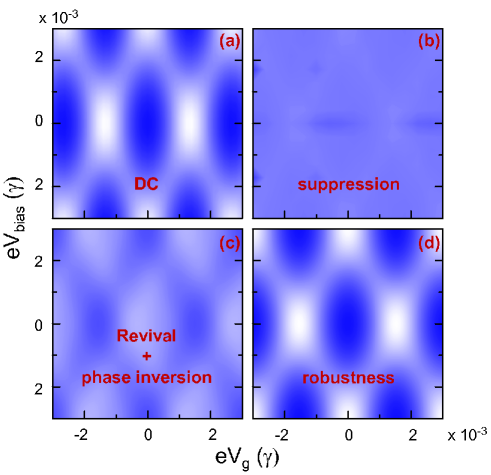
It can be noticed that remains unaffected by the AC potential while the amplitude is modulated by a factor of . Therefore, the oscillatory contribution is canceled whenever , i.e., the argument is a root of . In the following, we investigate how the whole interference patterns is affected choosing certain values of and which result in special transport conditions on those curves. For instance, we select the following AC parameters: (a) (only DC components), first (b) minimum and (c) maximum conductance and (d) constant transmission on the curve .
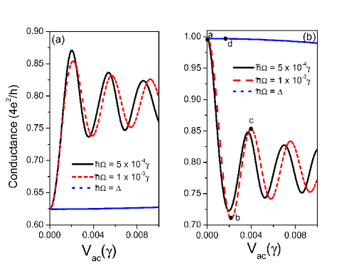
The panels 4 show how the full FP interference patterns of an AGNR interferometer change under the influence of an AC driven field being its intensity and frequency values marked on Fig. 3 by the letters (a), (b), (c) and (d). The diagram (a) corresponds to the DC pattern already addressed on the previous section. These characteristic oscillations are entirely suppressed when the AC field is driven to the minimum point (b) followed by a partial revival and a phase inversion when the perturbation is led to situation (c). Finally, an identical DC FP diagram is recovered when , and this reflects in a robustness feature of the system. Therefore, depending on how the AC parameters are tuned, it is possible to invert the phase of the oscillations, to suppress or to recover them. This can be interpreted as a manifestation of wagon-wheel condition in the quantum domain as found for carbon nanotubes Torres2009 . We now demonstrate that AGNR also displays such quantum effect.
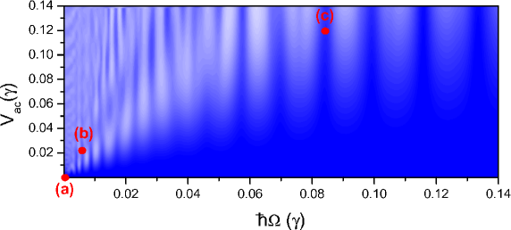
The overall behavior of the FP oscillations in AGNRs is displayed in the contour plots of Fig. 5 together with noise power results (). Blue corresponds to maximum values of conductance (noise) and white to minimum values. At low frequency, the results of Fig. 5-upper panel are in agreement with those given by the adiabatic theory and become independent of . On the other hand, at high frequencies [], deviations from the adiabatic regime are expected and the suppression of the oscillations is revealed for higher values of . Very well defined regions matching with multiples of the energy spacing level can be also identified from the plots. As previously stated, whenever being an integer, the patterns are insensitive to the AC field even under variations of .
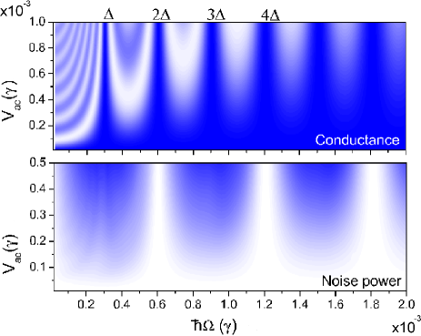
In contrast with the conductance, we find that the noise power (Fig. 5-lower panel) does not behave as in the static case whenever the whagon-wheel condition is met. In fact, the suppression of the noise takes place when the frequency is commensurate with an even multiple of the level spacing. This is a consequence of the fact that the noise under AC fields is highly sensitive to the phase of the transmission amplitude which changes by over each resonance. In between these minima, there are local maxima whose intensity is proportional to . Summarizing, the noise recovers the static response whenever being an integer. This behaviour is the same as the one found for and in particular for metallic nanotubesTorres2009 where this effect was interpreted as a manifestation of the wagon-wheel condition in which the static noise behaviour requires a doubling of the stroboscopic frequency. This occurrence may result in important technological applications since it is possible to combine high transmission states with low current noise.
Under DC conditions, ZGNR already presented richer interference patterns mainly due to its non-linear dispersion around the flat state. Combining this highly dense spectrum nearby the Fermi energy with the application of an external AC driven field, high order photonic transitions might take place resulting in a even more complicated pattern, specially in the low frequency range. This can be seen in the AC contour-plot of Fig. 6 which shows the conductance as a function of the parameters of the driving field. As the frequency increases, a more regular pattern emerges, showing the same equally spaced segments associated with a characteristic energy level spacing. A characteristic frequency determining the crossover to the regular FP patterns can be estimated from the plot. In the following, we present the whole FP-diagrams [Figs. 7(a) and (b)] when the driving field lies on the particular points (a) and (b) marked on the contour-plot. The complexity of diagram 7(a) obtained at adiabatic regime is remarkable while the robustness is evidenced once more in Fig. 7(b). These thinner structures can also be eliminated by temperature in a experimental procedure and for this reason we expect that this oscillations can only be observed at high frequency limit.
II.3 Scaling of the current noise with the ribbons length and width
Geometric aspects such as width and length of the nanoribbon can affect significantly the AC transport properties. For simplicity, we restricted this investigation to AGNRs due to their more regular responses and hence they seem to suite better to applications in electronic nanodevices. Increasing the sample length reduces the level spacing and then the noise is suppressed whenever the wagon-wheel condition is met. We find that the lower limit for the frequencies required to achieve this effect is in the order of . As for the scaling with the width, we observed a ten percent increase in the current noise for widths of about nm for THz frequencies. This small effect is observed as a result of the onset of a contribution due to higher subbands. This occurs when inelastic processes can produce excitations that allow to tunnel over the gap of the corresponding massive subband, thereby representing a contribution to the noise from electrons deep in the Fermi sea.
III Conclusions
By combining a tight-binding model with a Floquet solution we have solved for the electronic transport properties of ac-gated graphene nanoribbons in the Fabry-Perot regime. In contrast to carbon nanotubes, the interference pattern for nanoribbons depends strongly on the shape of the edges. For armchair edges, the results coincide with those obtained for nanotubes and a detailed derivation of both current and noise properties was presented. The time-dependent field can be tuned such that the Fabry-Perot oscillations become smoother, invert their phase, recover the original DC features or even suppress them. Moreover, whenever is an even multiple of the mean level spacing it is possible to achieve states of high conductance with low current noise (quantum wagon-wheel effect). These calculations for armchair edges greatly benefitted from a mode decomposition which allows a drastic reduction of the computational time (see Appendix IV). On the other hand, for zigzag-edges the non-linear energy dispersion nearby the flat band causes significant changes on the interference patterns making reasonably easy to distinguish between these two graphene edge structures. Regular Fabry-Perot oscillations are only visible at high bias/gate potentials.
Our work is a first step towards the understanding of the interplay between quantum interference and ac driving in graphene systems. Further research aimed at the study of quantum pumping in these systems is in progress.
Acknowledgments. This work was supported by the Alexander von Humboldt Foundation, by the European Union project “Carbon nanotube devices at the quantum limit” (CARDEQ) under contract No. IST-021285-2. Computing time provided by the ZIH at the Dresden University of Technology is also acknowledged. We acknowledge Dr. Miriam del Valle for the valuable discussions.
IV Appendix A: Eigenchannel/Mode decomposition for graphene nanoribbons
Solving brute force the Hamiltonian to obtain the transport properties of pristine graphene (armchair edge) nanoribbons, even by using a decimation procedure, is computationally very expensive. In the following we detail a way to substantially reduce the calculation size of the problem along the lines of previous work carried out for nanotubes Mingo2001 and also for graphene Zhao2009 . The eigenchannel or mode decomposition scheme proposed below is based on a very simple idea: rewriting the Hamiltonian in a basis that privileges the eigenstates in the direction perpendicular to the transport direction.
In an AGNRS, layers of A-type and B-type atoms alternate along the transport direction. Considering the interaction between the atoms in these layers, the Hamiltonian can be written in the block form:
| (8) |
where is the block corresponding to atoms in the layer and and are the ones connecting layers of different type. While has a canonical form, , the matrix can be written as:
| (9) |
Note that for the case of carbon nanotubes the top right matrix element, , is equal to . As argued below, this introduces a major difference between the (zig-zag) CNT and the (armchair) GNR cases: the lack of this periodic boundary condition breaks the translational symmetry along the axis perpendicular to the transport direction.
The case of zigzag CNTs. In this case the matrix can be diagonalized, i.e., there is a () matrix such that has a diagonal form. Since commutes with and the change of basis transformation:
gives a block tri-diagonal representation of the Hamiltonian. Each of these blocks correspond to an independent mode that can be represented by a tight-binding chain with alternating hoppings and ().
The case of armchair GNRs. In contrast to the case of zigzag tubes, the matrix [Eq. (9)] cannot be diagonalized. Therefore, a different strategy is necessary. Inspired by the geometrical arrangement of the A and B sublattices, an alternative basis transformation can be adopted:
where the arrangement of the matrices and is periodically repeated with a four layer periodicity (same as the lattice). The matrix elements of and are chosen to satisfy hard boundary conditions:
| (10) |
| (11) |
Interestingly, the blocks of the transformed Hamiltonian are all diagonal. Indeed, the blocks proportional to the identity matrix remain invariant ( ), while Therefore, the graphene armchair nanoribbon can be represented as independent one dimensional chains with alternating hoppings and being .
V Appendix B: Analytical results for the current noise at the wagon-wheel condition
Here we show that for a driven system with a constant level spacing, the current noise vanishes whenever the frequency is commensurate with twice the level spacing. We call this modified wagon-wheel or stroboscopic condition, the quantum wagon-wheel condition.
In the following let us consider a single mode. Then, for perfectly homogeneous driving the noise power (zero frequency component of the current-current correlation function) can be written according to Eq. (4) Kohler2005 .
In our case, the above expression is the contribution from only one of the modes in the mode decomposition scheme. However, close to the charge neutrality point, only two modes contribute. Furthermore, due to symmetry reasons, their contribution is the same.
Further analysis of the Green functions reveals that for a system with a constant level spacing the local Green function is periodic with a period equal to the level spacing In contrast, (whose phase determines the transmission phase shift which changes by through each resonance) has a period of . These two facts combined with the use of the identity gives as in the static case. It is interesting to notice that although the conductance at and are the same, the noise vanishes only in the latter case. This gives interesting prospects for achieving maximum interference amplitude with minimum noise in a driven system, much in consonance with Ref. strass2005 .
A similar behavior is expected whenever the identity is approximately fulfilled. This is the case for example when giving rise to the features observed in Fig. 5 in the vicinity of (odd ) and small .
References
- (1) G. Platero and R. Aguado, Phys. Rep. 395, 1 (2004).
- (2) S. Kohler, J. Lehmann, and P. Hänggi, Phys. Rep. 406, 379 (2005).
- (3) M. Büttiker, J. Low Temp. Phys., 118, 519 (2000).
- (4) D. J. Thouless, Phys. Rev. B 27, 6083 (1983).
- (5) B. L. Altshuler and L. I. Glazman, Science 283, 1864 (1999).
- (6) M. Switkes et al., Science 283, 1905 (1999); B. Kaestner et al., Phys. Rev. B 77, 153301 (2008).
- (7) E. Prada, P. San-Jose, and H. Schomerus, arXiv:0907.1568v1 (unpublished)
- (8) F. Grossmann et al., Phys. Rev. Lett. 67, 516 (1991).
- (9) J.-C. Charlier, X. Blase, and S. Roche, Rev. Mod. Phys. 79, 677 (2007); R. Saito, G. Dresselhaus, and M.S. Dresselhaus, Physical Properties of Carbon Nanotubes (Imperial College Press, London, 1998).
- (10) K. S. Novoselov et al., Science 306, 666 (2004).
- (11) M.Y. Han, B. Özyilmaz, Y. Zhang, and P. Kim, Phys. Rev. Lett. 98, 206805 (2007).
- (12) A.H. Castro Neto, F. Guinea, N.M.R. Peres, K.S. Novoselov, and A.K. Geim, Rev. Mod. Phys. 81, 109 (2009)
- (13) C. G. Rocha, A. Wall, M. S. Ferreira, EPL 82, 27004 (2008); O. V. Kibis, M. Rosenau da Costa, and M. E. Portnoi, Nano Letters 7, 3414 (2007).
- (14) M. del Valle, R. Gutierrez, C. Tejedor and G. Cuniberti, Nat. Nanotech. 2, 176 (2007).
- (15) J. C. Coiffic et al., Appl. Phys. Lett. 91, 252107 (2007).
- (16) F. Miao, et al. Science 317, 1530 (2007).
- (17) W. Liang et al., Nature 411, 665 (2001).
- (18) For a review on noise in mesoscopic conductors see Ya. M. Blanter and M. Büttiker, Phys. Rep. 336, 1 (2000).
- (19) F. Wu et al., Phys. Rev. Lett. 99, 156803 (2007).
- (20) L. G. Herrmann et al. Phys. Rev. Lett. 99, 156804 (2007)
- (21) Na Young Kim et al., Phys. Rev. Lett. 99, 036802 (2007).
- (22) P. A. Orellana and M. Pacheco, Phys. Rev. B 75, 115427 (2007).
- (23) L. Oroszlany, V. Zolyomi, and C. J. Lambert, arXiv:0902.0753 (unpublished).
- (24) B. Trauzettel, Y. M. Blanter, and A. F. Morpurgo, Phys. Rev. B 75, 035305 (2007).
- (25) S. V. Syzranov, M. V. Fistul, and K. B. Efetov, Phys. Rev. B 78, 045407 (2008).
- (26) F. J. López-Rodríguez and G. G. Naumis, Phys. Rev. B 78 201406 (2008).
- (27) S. E. Shafranjuk,J. of Phys.: Cond. Matt. 21, 015301(2009).
- (28) T. Oka and H. Aoki, Phys. Rev. B 79, 081406(R) (2009).
- (29) P. H. Rivera, A. L. C. Pereira, and P. A. Schulz, Phys. Rev. B 79, 205406 (2009).
- (30) R. Danneau, et al., Phys. Rev. Lett. 100, 196802 (2008).
- (31) S. E. Shafranjuk, arXiv:0809.4474.
- (32) A. R. Wright, J. C. Cao, C. Zhang, arxiv:0905.4304v1.
- (33) D. S. L. Abergel, T. Chakraborty, arxiv:0905.4522v1.
- (34) A. Cresti et al., Nano Research 1, 361 (2008).
- (35) Wen Long, Qing-feng Sun, and Jian Wang, Phys. Rev. Lett. 101, 166806 (2008)
- (36) B. Biel, X. Blase, F. Triozon, and Stephan Roche, Phys. Rev. Lett. 102, 096803 (2009)
- (37) L. E. F. Foa Torres, and G. Cuniberti, Appl. Phys. Lett. 94, 222103 (2009).
- (38) S. Krompiewski, J. Martinek, and J. Barnas, Phys. Rev. B 66, 073412 (2002).
- (39) M. Guigou, et al., , Phys. Rev. B 76, 045104 (2007).
- (40) B. H. Wu and J. C. Cao, arxiv:0906.5266v1 (unpublished).
- (41) S. Camalet, J. Lehmann, S. Kohler, and P. Hänggi, Phys. Rev. Lett. 90, 210602 (2003).
- (42) L. E. F. Foa Torres, Phys. Rev. B 72, 245339 (2005).
- (43) P. K. Tien and J. P. Gordon, Phys. Rev. 129, 647 (1963)
- (44) M. Moskalets and M. Büttiker, Phys. Rev. B 66, 205320 (2002).
- (45) A. Agarwal and D. Sen, J. Phys. Cond. Matt. 19, 046205 (2007).
- (46) Jinshuang Jin, Xiao Zheng, and YiJing Yan, J. Chem. Phys. 128, 234703 (2008); X. Zheng, J. Luo, J. Jin, and Y. Yan, J. Chem. Phys. 130, 124508 (2009).
- (47) G. Stefanucci, S. Kurth, A. Rubio, and E. K. Gross, Phys. Rev. B 77, 075339 (2008).
- (48) H. M. Pastawski, Phys. Rev. B 46, 4053 (1992).
- (49) A.-P. Jauho, N. S. Wingreen, and Y. Meir, Phys. Rev. B 50, 5528 (1994).
- (50) L. Arrachea, Phys. Rev. B 72, 125349 (2005).
- (51) M. Strass, P. Hänggi, and S. Kohler, Phys. Rev. Lett. 95, 130601 (2005)
- (52) N. Mingo, Liu Yang, Jie Han, and M. P. Anantram, Phys. Status Solidi B 226, 79 (2001).
- (53) P. Zhao et al., J. Appl. Phys. 105, 034503 (2009)