Cluster Imaging
with a Direct Detection CMOS Pixel Sensor
in Transmission Electron Microscopy
Abstract
A cluster imaging technique for Transmission Electron Microscopy with a direct detection CMOS pixel sensor is presented. Charge centre-of-gravity reconstruction for individual electron clusters improves the spatial resolution and thus the point spread function. Data collected with a CMOS sensor with 9.59.5 m2 pixels show an improvement of a factor of two in point spread function to 2.7 m at 300 keV and of a factor of three in the image contrast, compared to traditional bright field illumination.
keywords:
Monolithic active pixel sensor, Transmission Electron Microscopy;, , ,
1 Introduction
The use of radiation-tolerant CMOS active pixel sensors (APS) [1, 2] for direct detection in Transmission Electron Microscopy (TEM), opens new opportunities for fast imaging with high sensitivity [3, 4, 5, 6, 7]. One of the key figures of merit for a TEM imaging sensor is the point spread function (PSF), which affects both the imaging resolving capabilities of the sensor and the absolute image contrast [8]. The PSF of a pixellated APS used in direct detection depends on several parameters of which the most important are the pixel size, the electron multiple scattering in the sensor and the charge carrier diffusion in the active layer. This letter discusses the PSF achieved using an APS in two different regimes.
In traditional bright field illumination, the electron flux is such that each pixel is illuminated by one or more electrons per acquisition frame. In this regime the point spread function has a contribution from the lateral charge spread due to charge carrier diffusion in the active volume. Since the epitaxial layer of a CMOS APS is nearly field-free, charge carriers reach the collection diode through thermal diffusion, with collection times of . The typical cluster size for a CMOS APS with 10 m pixels is 4-5 pixels for 300 keV electrons and about 45 % of the charge is collected on the central pixel of the cluster. With bright field illumination, at high rate, the signal recorded on each individual pixel is the superposition of the charge directly deposited by a particle below the pixel area with that collected from nearby pixels through diffusion, multiple scattering and backscattering from the bulk Si. If the electron rate is kept low enough so that individual electron clusters can be reconstructed, a new regime of operation becomes available. The electron impact position is reconstructed by calculating the centre-of-gravity of the observed pulse heights on the pixels in the cluster. For pixel detectors with pixel pitch this technique makes it possible to obtain an point resolution in tracking applications for accelerator particle physics. The same technique can now be adopted for imaging, provided electron fluxes are low enough so that the detector occupancy is 0.05, and individual clusters can easily be resolved. Under these conditions the PSF is expected to depend only on the detector pixel size and cluster S/N (determining the single point resolution) and on multiple scattering. The image is reconstructed by combining a large number of frames, each giving 2-5 m accuracy for 0.01-0.05 % of the field of view, provided the frame rate is much faster than the dynamics being observed on the sample. In this paper we refer to this technique as “cluster imaging”.
2 Cluster Imaging Tests
The principle of cluster imaging for TEM has been tested using the TEAM1k CMOS monolithic pixel sensor, developed as part of the the multi-institutional TEAM (Transmission Electron Aberration-corrected Microscope) project [9]. The TEAM1k sensor and its performance will be discussed in details in a forthcoming paper on this Journal [10]. The chip is produced in the AMS 0.35 m CMOS-OPTO process and has a 1,0241,024 pixel imaging area with pixels arrayed on a 9.5 m pitch. The detector employed in this test has been back-thinned to 50 m and mounted on a carrier circuit board which is cut out below its active area to minimise back-scattering effects. A 75 m-diameter Au wire is mounted along the pixel rows on top of the sensor at a distance of 2 mm above its surface. Tests have been conducted with the sensor installed at the bottom of a FEI Titan microscope column at the National Center for Electron Microscopy (NCEM).
The energy deposited by electrons in the sensor active layer and the lateral charge spread are simulated with the Geant-4 program [12] using the low-energy electromagnetic physics models [13]. The CMOS pixel sensor is modelled according to the detailed geometric structure of oxide, metal interconnect and silicon layers. Electrons are incident perpendicular to the detector plane and tracked through it. Charge collection in the sensor is simulated with PixelSim, a dedicated digitisation module [14]. The simulation has the diffusion parameter , used to determine the width of the charge carrier cloud, free. Its value is extracted from data by a fit to the pixel multiplicity in the clusters of 300 keV electrons, where multiple scattering is lower. We find = (14.5) m, which is compatible with the value obtained for 1.5 GeV s in a prototype sensor with 2020 m2 pixels produced in the same CMOS process [11]. The response to single electrons is characterised in terms of the cluster size. We operate with a flux of 50 mm-2 frame-1 which allows us to resolve individual electrons. Electron hits are reconstructed as clusters of pixels. A clustering algorithm with two thresholds is used [7]. First the detector is scanned for “seed” pixels with pulse height values over S/N threshold set to 3.5. Seeds are sorted according to their pulse heights and the surrounding neighbouring pixels are added to the cluster, if their S/N exceeds 2.5.
 |
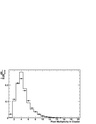 |
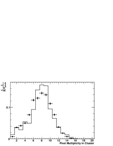
The pixel multiplicity at different electron energies is shown in Figure 1. The agreement of the tuned PixelSim simulation with data is good and we observe an increase of multiplicity at lower energies, as expected from the increased multiple scattering and energy deposition. The electron point of impact is determined from the position of the pixels in the cluster weighted by their pulse height. The average cluster S/N in data is 17 at 300 keV and 42 at 80 keV, due to the increase of the electron energy loss. The electron position of impact is computed as the centre-of-gravity of the charge recorded in the cluster. The Geant-4 + PixelSim simulation, which correctly reproduces the cluster signal pulse height and pixel multiplicity, predicts a point resolution for this reconstruction method of (6.750.15) m and (2.800.04) m for 80 keV and 300 keV electrons, respectively. As the energy decreases, multiple scattering in the inactive layers above the epitaxial layer increases, degrading the PSF. Better position resolution is obtained in particle physics applications, as the particles are more energetic.
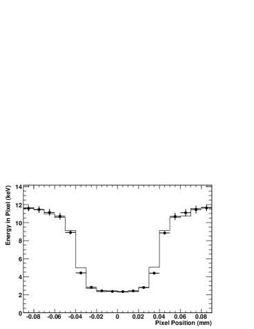
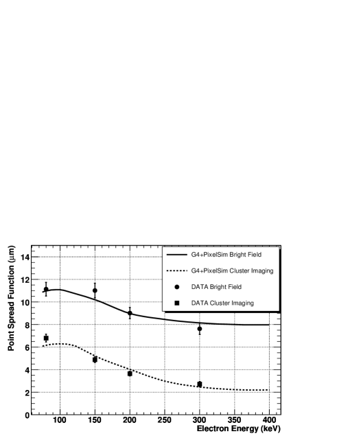
We compare the cluster imaging technique to bright field illumination, using the same detector, as a function of the electron energy. The PSF is measured on data along one coordinate from the image projected onto the sensor by the thin Au wire as discussed in [7]. Since the Au wire has well-defined edges, the profile of the deposited energy in the pixels, measured across the wire in bright field illumination allows us to study the lateral charge spread due to scattering and diffusion along the projected image of the edges. The electron flux is approximately 5103 e- mm-2 frame-1. The line spread function (LSF) is extracted by parameterising the measured pulse height on pixel rows across the wire image with a box function smeared by a LSF Gaussian term. The average pulse height level for pixels away from the wire region and the contrast ratio to the response below the wire are fixed to those observed in data and the LSF value is obtained by a simple 1-parameter fit with the Gaussian width as free parameter. At 300 keV, we measure a LSF value of (7.60.5) m which becomes (11.10.6) m at 80 keV, where the uncertainty include statistics and systematics from the result stability across the columns of a sector.
 |
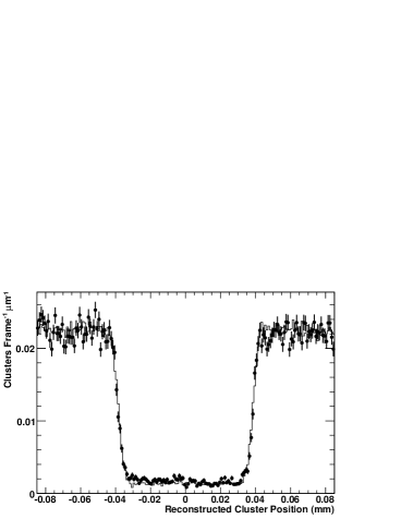 |
For cluster imaging, the electron flux is reduced to 50 e- mm-2 frame-1 and 20000 subsequent frames are acquired at each energy. Figure 2 shows the image of the wire obtained in the two regimes. With cluster imaging, due to the continuous spatial sampling, the information is no longer discretised by the pixel pitch as it is with bright field illumination. Charge diffusion, which limits the PSF in bright field illumination, now rather improves the cluster resolution by spreading the charge on more pixels and the relevant parameter for PSF becomes the ratio of pixel pitch to signal-to-background, which determines the cluster spatial resolution. We also observe that the image contrast improves by a factor of three for cluster imaging compared to bright field illumination, as it is apparent in Figure 2. The LSF is extracted by a fit, as discussed above. We measure (2.720.25) m at 300 keV, (3.650.20) m at 200 keV and (6.800.35) m at 80 keV. These results show that cluster imaging improves the point spread function by a factor of two compared to traditional bright field illumination, for the TEAM1k detector parameters. We perform the study on simulation describing the detector and wire geometry, for both operation regimes and compare the results to the measured LSF values. Results are summarised in Figure 3. Simulation reproduces well the data both in absolute terms and in the observed scaling with the electron energy. We also note that the cluster imaging LSF closely follows the simulation predictions for single point resolution.
3 Conclusions
The TEAM CMOS APS has demonstrated a PSF for direct detection under bright field illumination comparable to its pixel size. Image reconstruction by clustering at the impact point of individual electrons at low flux allows to reduce the PSF down to (2.720.25) m and improves the image contrast. In order to practically exploit this method in TEM it is necessary to ensure that the sensor can be read out at a rate of several hundred frames s-1 and cluster reconstruction can be performed in real time.
Acknowledgements
This work was supported by the Director, Office of Science, of the U.S. Department of Energy under Contract No.DE-AC02-05CH11231. The TEAM Project is supported by the Department of Energy, Office of Science, Basic Energy Sciences.
References
- [1] E.R. Fossum, IEEE Trans. Electron. Devices 44 (1997) 1689.
- [2] R. Turchetta et al., Nucl. Instrum. and Meth. A 458 (2001) 677.
- [3] A.-C. Milazzo et al, Ultramicroscopy 104 (2005) 152.
- [4] G. Deptuch et al., Ultramicroscopy 107 (2007) 674.
- [5] P. Denes et al. Nucl. Instrum. Meth. A 579 (2007) 891.
- [6] G.Y. Fan et al., Ultramicroscopy 70 (1998) 113.
- [7] M. Battaglia et al., Nucl. Instr. Meth. A 598 (2009) 642 [arXiv:0811.2833 [physics.ins-det]].
- [8] A. Thust, Phys. Rev. Lett. 102 (2009) 220801.
- [9] U. Dahmen, Microscopy and Microanalysis 13 (2) (2007) 1150.
- [10] M. Battaglia et al., to be submitted to Nucl. Instr. Meth. A.
- [11] M. Battaglia et al., Nucl. Instr. Meth. A 605 (2009) 350 [arXiv:0904.0552 [physics.ins-det]].
- [12] S. Agostinelli et al., Nucl. Instrum. Meth. A 506 (2003) 250.
- [13] S. Chauvie et al., Prepared for CHEP’01: Computing in High-Energy Physics and Nuclear, Beijing, China, 3-7 Sep 2001.
- [14] M. Battaglia, Nucl. Instrum. Meth. A 572 (2007) 274.