Multi-band conductivity and multi-gap superconductivity in V3Si from optical measurements on films at terahertz frequencies
Abstract
The possibility of multi-band conductivity and multi-gap superconductivity is explored in oriented V3Si thin films by means of reflectance and transmittance measurements at terahertz frequencies. The temperature dependence of the transmittance spectra in the normal state gives evidence of two bands contributing to the film conductivity. This outcome is consistent with electronic structure calculations performed within density functional theory. On this basis, we performed a detailed data analysis and found that all optical data can be consistently accounted for within a two-band framework, with the presence of two optical gaps in the superconducting state corresponding to 2 values close to 1.8 and 3.8.
pacs:
74.70.Ad, 74.25.Gz, 78.30.-jLarge interest has been devoted Bouquet02 ; Mazin03 to multi-band superconductivity after the discovery of two bands with two distinct superconducting gaps in MgB2 Kortus01 . Very recently, the interest in multi-band superconductivity has been renewed Moreo by the discovery of the Fe-As based superconductors, where the presence of multiple bands is well established Maz08 . It is worth noting that two-gap superconductivity has been considered theoretically since the fifties Suh59 , and experimentally observed in transition metals Viel66 , in the A15 compound Nb3Sn Broc69 ; Gur04 and in MgCNi3 Walt04 . However, only after the discovery of superconductivity in MgB2, clear cut evidence of two-gap superconductivity and of its implications was obtained, since in this compound the multi-band, multi-gap character is emphasized by the exceptionally low inter-band scattering Maz02 .
In the case of the A15 V3Si system, a spread in the gap values corresponding to 2 extending from 1.0 to 3.9 has been reported in the past Tanner73 ; Mit86 . Recently, the electrodynamic response in the microwave region gave evidence of two gaps Nef05 , while muon spin rotation measurements were consistent with a single-gap model Cal05 . It is also worth noting that V3Si has been recently treated as a two-band system Hauptmann09 ; Kogan09 , but existing band structure calculations Klein78 ; Borg89 do not provide detailed enough information.
In this contradictory scenario, we investigate in the present work the possible two-band, two-gap character of V3Si, by performing both an infrared spectroscopy study and electronic structure calculations within density functional theory (DFT).
Infrared (IR) spectroscopy is a powerful tool to study the properties of a conducting system. In the normal state (N-state), the Drude model for the frequency-dependent complex conductivity can be employed to describe the optical response of free-charge carriers Burns . As shown in the MgB2 case Kuz07 ; Ort08 , it is thus possible to determine the contributions of different -bands and thus the corresponding plasma frequencies and scattering rates . In the superconducting state (S-state), on the basis of the BCS model for the complex conductivity Tink , far-IR/terahertz measurements can be of particular importance since a mark of the superconducting gap can be observed at (optical gap) for an isotropic -wave BCS superconductor. In particular, a maximum at the optical gap is expected either in the ratio (for a bulk sample) or in the ratio (for a thin film), where () and () are the frequency-dependent reflectances (transmittances) in the S- and N- state, respectively Tink . In the MgB2 case Kuz07 , evidence of the two gaps was detected in the spectrum of an ultra-clean film Ort08 by assuming a parallel sum of the conductivity of two independent bands and by using the model introduced by Zimmermann et al. Zim91 which generalizes the BCS one to arbitrary and values (Zimmermann model).
We performed IR measurements on high-quality V3Si textured films. Details on the film growth by pulsed laser deposition and on their properties are reported elsewhere Ferd1 . We studied two films grown on LaAlO3 (LAO) (001) 0.5 mm thick substrates, which exhibit preferential (210) orientation along the out-of-plane direction. The first film of thickness =180 nm (film d180) has good transport properties (resistivity at 300 K close to 200 cm, residual resistivity ratio =8) and =16.1 K; the second film, 33 nm thick (film d033), has worst transport properties (=4.5) and a slightly lower value (=15.3 K).
We first performed measurements of the IR reflectance of film d180 as a function of temperature (not shown). The spectrum at 300 K is in very good agreement with the result of previous measurements Borg89 . We attempted an analysis of the measured spectra by including in the model a number of Lorentz contributions representing optically active inter-band transition. However, unambiguous results were not obtained since at any temperature a very broad Drude contribution Borg89 is partially overwhelmed by strong interband transitions occurring at rather low frequencies because of the complex electronic structure of V3Si Klein78 ; Borg89 .

We then measured the transmittance spectrum of film d033 by focusing the IR beam on the film or on a hole for reference. Measurements were performed between 300 and 20 K in the terahertz (THz) region (here defined by photon energies below 16 meV, frequency 130 cm-1 or THz), where the LAO substrate is partially transparent. spectra of film d033 are reported in Fig. 1a at selected temperatures, those of LAO Dore94 at the same temperatures in Fig.1b for comparison. The spectral shape of the 300 K spectrum is qualitatively similar to that of LAO as it monotonically increases with decreasing frequency, while the transmitted intensity is strongly reduced by the above discussed broad Drude contribution in the film conductivity. On the contrary, the spectral shape of the 20 K shows a broad maximum and then decreases with decreasing frequency. This result can be qualitatively explained by the presence of a second sharp Drude contribution, which narrows with decreasing temperature thus reducing the transmitted intensity at very low frequencies.
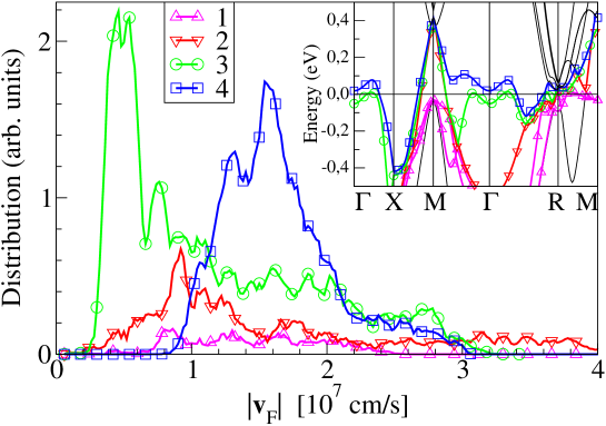
In order to better understand this result, we carried out electronic structure calculations within DFT on V3Si. We calculated the Fermi velocities starting from the energy bands shown in the inset of Fig.2. We used the experimental lattice constants and Chaddah83 , and calculated the dimerization of V chains along and directions to be . The Fermi level of V3Si is crossed by four bands (two bands with similar character and small density of states are grouped together) with mostly V character; with the chain direction along , orbitals and on one side and and on the other produce narrow and wide bands, respectively.
In Fig. 2 we plot the distribution of values of the moduli of Fermi velocities nota for the bands crossing ; the distributions are normalized to the densities of states of the same bands, so that the average squared velocity times the integral of the distribution provides, apart from numerical factors, the contribution to the square of the total plasma frequency eV. While it is difficult to assign a definite orbital character to each band throughout the whole Brillouin zone, we can see that the band separation naturally provides different average velocities, showing an overall bimodal distribution given by the bands n. 3 and 4, while the remaining bands provide a smaller contribution to plasma frequencies due to their smaller density of states. The bimodal distribution resulting from our calculations indicates that the V3Si conductivity in the N-state can be safely described in terms of two bands characterized by different values (two-band, 2-b model). It remains to be verified whether the presence of the two bands reflects in the opening of two distinct superconducting gaps, as in the MgB2 case.

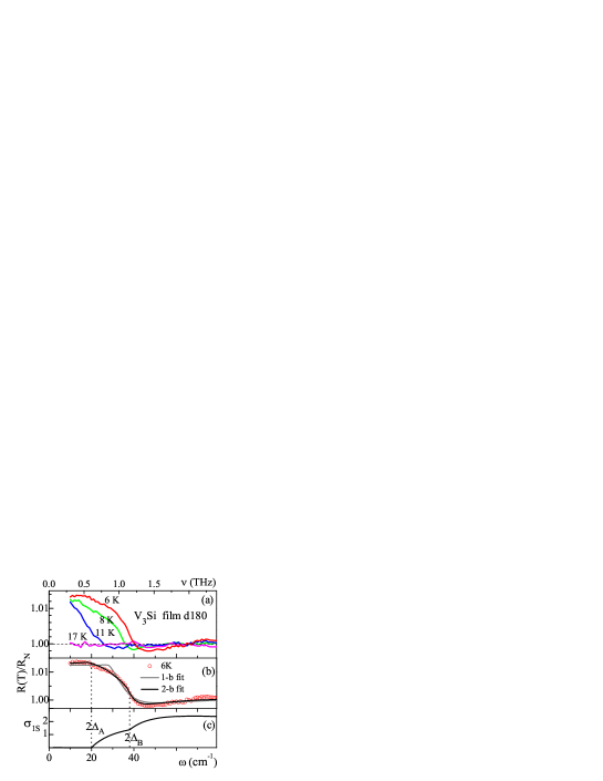
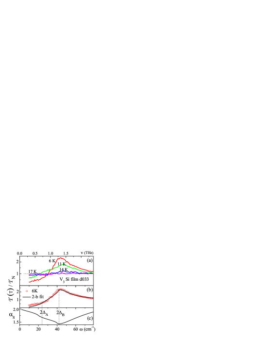
To this aim we measured at 20 K the (where (20 K)) spectra of the d180 film (see Fig.3a) and the (where (20 K)) spectra of the d033 film (see Fig.4a). These measurements were made by cycling the temperature in the 6-20 K range, without collecting reference spectra. In this way one avoids any variation in the sample position and orientation, which may yield frequency-dependent systematic errors in and Ort06 . All measurements in the THz region were made by employing synchrotron radiation at the infrared beamline SISSI SISSI at the synchrotron Elettra (Trieste, Italy) and at the BESSY storage ring (Berlin, Germany), where coherent synchrotron radiation is available Scha01 . We remark that a high-flux synchrotron source allows an high accuracy in the detection of small effects in the spectra, and overcomes the problem of the very low intensity transmitted by the film+substrate system in the case of transmission measurements on a conducting film. We also note that (where (6 K)) is affected by the superconducting transition much more than (where (6 K)) since the transmitted intensity is dominated by the effect of the absorptive processes in the film, which significantly changes below Tink ; Will90 .

We first notice that the spectrum increases on decreasing temperature (see Fig. 3a), until reaches a maximum and becomes nearly constant below 20 cm-1. This indicates the presence of a superconducting gap close to 10 cm-1. Indeed, for , the reflectance of a conducting system tends to 1 for a bulk system, to a slightly lower value for a thin film. Therefore, since approaches 1 at , exhibits a maximum around in the case of a bulk sample, remains nearly constant below in the film case. As to the data (see Fig. 4a), a maximum develops on decreasing until the exhibits a well defined peak around 40 cm-1, which indicates the presence of a superconducting gap around 20 cm-1.

For a detailed analysis of the measured spectra based on the 2-b model, the conductivity of V3Si can be described by the sum of two Drude terms in the N-state (, with parameters , ), and by the sum of two Zimmermann terms in the S-state, as discussed above (, with parameters , , ). From , by using standard relations Burns , it is possible to compute the model refractive index of V3Si in both the N- and S-state. The transmittance and reflectance spectra of the film+substrate system in both states can then be evaluated by means of an exact procedure Berb93 which requires, besides thickness, numerical values of and for both film and substrate. For LAO, and values in the THz region were obtained from previous measurements of transmittance and reflectance of a LAO substrate Dore94 through a numerical, model independent procedure Cuns92 .
We first analyzed the spectrum, by performing a 6 parameter fit (,, , ). The best-fit curve does well describe experimental data, as shown in Fig.3b. By keeping into account the uncertainties resulting from the fitting procedure, we can safely pose eV, eV, cm-1, cm-1, cm-1, and cm-1. We verified that unsatisfactory results are obtained by considering one band only (one-band, 1-b model). Note that, in the 2-b approach, the A-band contribution has a crucial effect, as it gives a vanishing only below 2 (see Fig.3c). Since, in general, approaches 1 when vanishes, this explains why only the gap is well evident in the spectrum.
In order to verify the compatibility of this fit with first principle results, we calculated plasma frequencies from our Fermi velocities. In particular, we integrated over the Brillouin zone separating the low and high regions (setting an arbitrary but plausible cutoff at 107 cm/s; see Fig.2). While this procedure is only qualitative, it may be justified by the presence of clearly separable ranges of , in turn deriving from different orbital natures. We obtain =3.21 eV and = 0.81 eV. In comparing these results with those of the fitting procedure, it is worth noting that the best-fit values of and , and thus of , can be overestimated because the interband transitions discussed above may give non negligible contributions to even at very low frequencies. This effect is minimized in the best-fit / ratio (3.70.3), which results to be in a remarkably good agreement with the computed one (3.96).
In analysing the transmittance spectra of film d033, we verified that only the 2-b model well describes at all temperatures, but the resulting and values are not unambiguously determined. We thus used a procedure which simultaneously fits both and , thus imposing important constraints in the fitting procedure. Good fits of both (see Fig.1b) and (see Fig.4b) were obtained, with values slightly lower, values slightly higher than those found in fitting the spectrum. This can be simply explained by the worse conducting properties of film d033 with respect to film d180. As to the gap values, nearly equivalent fits are obtained for ranging from 11 to 16 cm-1, while = 21.0 0.5 cm-1 is well determined since it corresponds to the peak in . The transmission measurement, dominated by the absorption process, thus permits to unambiguously establish the value which was more poorly defined in the measurement. The higher sensitivity of to the gap is a consequence of the frequency dependence of the absorption coefficient of V3Si in the S-state. Indeed, , as evaluated with standard relations Burns through the 2-b model, only exhibits a well defined minimum around 2 (see Fig.4c).
In summary, we addressed the debated problem of multi-band, multi-gap nature of V3Si by means of reflectance and transmittance measurements in the THz region on high quality oriented films. Experimental results indicate the presence of two bands contributing to the V3Si conductivity in the normal state, and of two optical gaps in the superconducting state. Electronic structure calculations within density functional theory showed that the distribution of the modulus of the Fermi velocity exhibits a clear bimodal character, which indicates that the V3Si conductivity in the normal state can be safely described in terms of two bands, characterized by different plasma frequencies. On this basis, we performed a detailed data analysis and found that all optical data can be consistently accounted for within a two-band framework, with the presence of two optical gaps corresponding to 2 values close to 1.8 and 3.8.
The authors acknowledge M. Prasciolu for preparing the Au reference surface used in the absolute reflectance measurements.
References
- (1) F. Bouquet, Y. Wang, I. Sheikin, T. Plackowski, A. Junod, S. Lee, and S. Tajima, Phys. Rev. Lett. 89, 257001 (2002)
- (2) I.I. Mazin and V.P. Antropov, Physica C 385, 49 (2003)
- (3) J. Kortus, I.I. Mazin, K.D. Belashchenko, V.P. Antropov, and L.L. Boyer, Phys. Rev. Lett. 86, 4656 (2001)
- (4) A. Moreo, M. Daghofer, A. Nicholson, and E. Dagotto, arXiv:0906.1747
- (5) I.I. Mazin, D.J. Singh, M.D. Johannes, and M.H. Du, Phys. Rev. Lett. 101, 057003 (2008)
- (6) H. Suhl, B.T. Matthias, and L.R. Walker, Phys. Rev. Lett. 3, 552 (1959).
- (7) L.J. Vieland and A.W. Wicklund, Phys. Rev. 166, 424 (1968).
- (8) J.C.F. Brock, Solid State Commun. 7, 1789 (1969)
- (9) V. Guritanu, W. Goldacker, F. Bouquet, Y. Wang, R. Lofiz, G. Goll and A. Junod, Phys. Rev. B 70, 184526 (2004)
- (10) A. Walte, G. Fuchs, K.-H. Muller, A. Handstein, K. Nenkov, V.N. Narozhnyi, S.-L. Drechsler, S. Shulga, L. Schultz, and H. Rosner, Phys. Rev. B 70, 174503 (2004).
- (11) I.I. Mazin, O.K. Andersen, O. Jepsen, O.V. Dolgov, J. Kortus, A.A. Golubov, A.B. Kuzmenko, and D. Van Der Marel, Phys. Rev. Lett. 89, 107002, (2002).
- (12) D.B. Tanner and A.J. Sievers, Phys. Rev. B 8, 1978 (1973)
- (13) For a number of gap values measured in V3Si see: A.B. Mitrovic and J.P. Carbotte, Phys. Rev. B 26, 1244 (1982)
- (14) Y.A. Nefyodov, A.M. Shuvaev, and M.R. Trunin, Europhys. Lett. 72, 638 (2005).
- (15) F.D. Callaghan, M. Laulajainen, C.V. Kaiser, and J.E. Sonier, Phys. Rev. Lett. 95, 197001 (2005).
- (16) N. Hauptmann, M. Becker, J. Kröger, R. Berndt, Phys. Rev. B 79, 144522 (2009)
- (17) V.G.Kogan, C.Martin, and R.Prozorov, arXiv:0905.0029.
- (18) B.M. Klein, L.L. Boyer, D.A. Papaconstantopoulos, and L.F. Mattheiss, Phys. Rev. B 18, 6411 (1978).
- (19) A. Borghesi, A. Piaggi, G. Guazzetti, F. Nava, and M. Bacchetti, Phys. Rev. B 40, 3249 (1989).
- (20) G. Burns, Solid state physics, Academic Press, Boston (1990).
- (21) For a comprehensive review of infrared studies on MgB2, see: A.B. Kuzmenko, Phys. C 456, 63 (2007).
- (22) M. Ortolani, P. Dore, D. Di Castro, A. Perucchi, S. Lupi, V.Ferrando, M.Putti, I. Pallecchi, C. Ferdeghini, and X.X.Xi, Phys. Rev. B 77, 100507(R) (2008).
- (23) M. Tinkham, Introduction to Superconductivity, McGraw-Hill, New York (1975).
- (24) W. Zimmermann, E.H. Brandt, M. Bauer, E. Seider, and L. Genzel, Phys. C 183, 99 (1991).
- (25) C. Ferdeghini, E. Bellingeri, C. Fanciulli, M. Ferretti, P. Manfrinetti, I. Pallecchi, M. Putti, C. Tarantini, M. Tropeano, A. Andreone, G. Lamura, and R. Vaglio, IEEE Trans. Appl. Supercond. (in press, 2009).
- (26) P. Dore, G.P. Gallerano, A. Doria, E. Giovenale, R. Trippetti, and V. Boffa, Nuovo Cimento D 16, 1803 (1994).
- (27) P. Chaddah and R.O. Simmons, Phys. Rev. B 27, 119 (1983)
- (28) A similar distribution in terms of the components of would peak around zero due to geometrical factors.
- (29) M. Ortolani, S. Lupi, L. Baldassarre, U. Schade, P. Calvani, Y. Takano, M. Nagao, T. Takenouchi, and H. Kawarada, Phys. Rev. Lett. 97, 097002 (2006)
- (30) S. Lupi, A. Nucara, A. Perucchi, P. Calvani, M. Ortolani, L. Quaroni, and M. Kiskinova,JOSA B, 24, 959 (2007)
- (31) W.B. Peatman and U. Schade, Rev. Sci. Instr. 72, 1620 (2001)
- (32) G.P. Williams, R.C. Budhani, C.J. Hirschmugl, G.L. Carr, S. Perkowitz, B. Lou, and T.R. Young, Phys. Rev. B 41, 4752 (1990)
- (33) P. Berberich, M. Chiusuri, S. Cunsolo, P. Dore, H. Kinder, and C.P. Varsamis, Infrared Phys. 34, 269 (1993).
- (34) S. Cunsolo, P. Dore, and C.P. Varsamis, Applied Optics 31, 4554 (1992)