Universal zero-bias conductance through a quantum wire side-coupled to a quantum dot
Abstract
A numerical renormalization-group study of the conductance through a quantum wire side-coupled to a quantum dot is reported. The temperature and the dot-energy dependence of the conductance are examined in the light of a recently derived linear mapping between the Kondo-regime temperature-dependent conductance and the universal function describing the conductance for the symmetric Anderson model of a quantum wire with an embedded quantum dot. Two conduction paths, one traversing the wire, the other a bypass through the quantum dot, are identified. A gate potential applied to the quantum wire is shown to control the flow through the bypass. When the potential favors transport through the wire, the conductance in the Kondo regime rises from nearly zero at low temperatures to nearly ballistic at high temperatures. When it favors the dot, the pattern is reversed: the conductance decays from nearly ballistic to nearly zero. When the fluxes through the two paths are comparable, the conductance is nearly temperature-independent in the Kondo regime, and a Fano antiresonance in the fixed-temperature plot of the conductance as a function of the dot energy signals interference. Throughout the Kondo regime and, at low temperatures, even in the mixed-valence regime, the numerical data are in excellent agreement with the universal mapping.
pacs:
73.21.La,72.15.Qm,73.23.HkI Introduction
The transport properties of nanostructured devices constitute a complex subject. Amongst its numerous facets, interference is one of the shiniest, because it challenges classical intuition, adds colorful features to experimental plots, and can be controlled. Such characteristics have motivated numerous studies, in either the Aharonov-Bohm or the -shaped interferometric arrangement.Hofstetter et al. (2001); Aikawa et al. (2004); Aharony et al. (2006); Fuhrer et al. (2006); Dias da Silva et al. (2006, 2008); Bulka and Stefanski (2001); Clerk et al. (2001); Torio et al. (2002); Franco et al. (2003); Maruyama et al. (2004); Kobayashi et al. (2004); Sato et al. (2005); Zitko and Bonca (2006); Maruyama et al. (2006); Katsumoto (2007) The minimal number of components in and the rich variety of effects stemming from the latter setup make it particularly interesting.
The -shaped device comprises a quantum-dot side-coupled to a quantum wire, through which current flows in response to a small bias. Its dynamics parallels that of the single-electron transistor, the alternative arrangement that embeds the quantum dot in the conduction path. The same Hamiltonian models the two devices, the thermodynamical properties are hence identical. Nonetheless, the conductances in the two geometries are remarkably distinct.
In either geometry, if a gate potential applied to the quantum dot tunes its occupation to an odd integer, the resultant magnetic moment interacts antiferromagnetically with the wire electrons and induces a Kondo cloud. Thin at first, the cloud gradually shrouds the quantum dot as the temperature is reduced. Below the Kondo temperature , the cloud and dot moment lock into a singlet. In energy space, the Kondo resonance in the low-energy spectrum of the model Hamiltonian identifies the consolidation of the Kondo singlet.Hewson (1993)
The conductances of the single-electron transistor and of the -shaped devices respond differently to the Kondo resonance. In the embedded arrangement, the resultant strong coupling between the conduction and the dot electrons breaks through the Coulomb blockade to allow conduction. This remarkable low-temperature property of the single-electron transistor found precise mathematical expression in the early numerical renormalization-group (NRG) study by Costi, Hewson, and Zlatic,Costi et al. (1994) who described the temperature-dependent conductance for the spin-degenerate Anderson modelAnderson (1961) and showed that the conductance for the particle-hole symmetric model is a monotonically decreasing universal function of the temperature scaled by the Kondo temperature.
In the side-coupled geometry, instead of enhancing the conductance, the Kondo droplet obstructs transport through the wire. While the thin high-temperature cloud offers little resistance to electronic flow, low temperatures raise a Kondo blockade in the wire sector closest to the dot. In experimental arrangements allowing conduction only through the wire, the conductance through the -shaped device therefore rises with temperature. For the symmetric Anderson Hamiltonian, in particular, the conductance is complementary to the universal function : , where is the quantum conductance.Maruyama et al. (2006); Yoshida et al. (2009a) To emphasize the significance of this theoretical finding, we define the complementary symmetric conductance .
More ellaborate -shaped setups accommodate an alternative conduction path through the quantum dot, a bypass around the blocked wire segment.Kobayashi et al. (2004); Sato et al. (2005); Katsumoto et al. (2006) Considered on its own, the bypass is equivalent to a single-electron transitor: while a Coulomb blockade bars electronic transfer through the dot at high temperatures, the Kondo resonance allows conduction at low .
Most frequently, the two conduction paths coexist. Three conduction patterns then stem from the combination of the currents through them.Kobayashi et al. (2004); Sato et al. (2005); Katsumoto et al. (2006); Otsuka et al. (2007) If the experimental conditions favor the bypass (the path traversing the wire), the conductance will decay (rise) with temperature, following the pattern set by the universal (the complementary-conductance) function [].
The third pattern arises when the amplitudes for electronic transfer along the two paths are comparable. The conductance is then a relatively flat function of temperature, but the low-temperature conductance profile (i. e., as a function of the dot gate potential at fixed temperature) shows Fano antiresonances indicative of interference between the two currents. Under a variable gate potential applied to the quantum wire, the response of a -shaped device to a small bias can be adjusted to bring out any of the three patterns.Katsumoto et al. (2006); Otsuka et al. (2007)
Together with such experimental findings, theoretical analyses have contributed to our understanding of the -shaped device. Important results have been derived.Hofstetter et al. (2001); Maruyama et al. (2004); Torio et al. (2002); Franco et al. (2003); Maruyama et al. (2006); Dias da Silva et al. (2008) More recently, the present authors showed that the temperature-dependent Kondo-regime conductance can be mapped onto the universal function .Seridonio et al. (2009) The mapping is linear, its coefficient an universal function of the ground-state phase shift of the wire electrons. The conductance depends on the model parameters only by way of and . If the model parameters make (), in particular, it results that ) [].Seridonio et al. (2009)
Here, to bring to light the physical content of the universal mapping, we present essentially exact numerical-renormalization group (NRG) results for the conductance of the -shaped device as a function of the dot gate potential and temperature for various wire gate potentials. In correspondence with the experimental data, the numerical data display three patterns: the temperature dependence of the conductances can be close to one of the two universal functions and , or approximately constant; the corresponding low-temperature conductance profiles are uniformly close to zero, uniformly close to ballistic, or display Fano antiresonances, respectively.
The mapping to the universal function describes accurately each calculated temperature-dependent conductance in the Kondo regime and thus condenses in a simple expression the variety of thermal and dot-energy dependences in the numerical study. It shows, moreover, that much like the optical phase difference controls the fringes in a Michelson-Morley interferometer, the ground-state phase shift controls the interference between the bypass and the cross-wire currents. For (), the former (latter) is dominant, and []. For intermediate phase shifts, the interference between the two currents raises antiresonances. Since depends on the gate potentical applied to the wire, the three conduction patterns appear in succession as the potential grows.
This paper closes a quartet dedicated to the conductance for the Anderson model of a wire coupled to a quantum dot. References Yoshida et al., 2009a and Yoshida et al., 2009b discussed the embedded geometry, the former paper having derived the mapping between the conductance and the universal function , and the latter having presented NRG data to illustrate and to probe the accuracy of that mapping at the limits of the Kondo regime and beyond them. Reference Seridonio et al., 2009 derived the mapping for the -shaped device, and this report compares it with an NRG survey of the side-coupled geometry.
Our presentation is divided in 5 sections. Section II defines the model Hamiltonian and recalls basic concepts associated with it. The mapping is discussed in Section III. The comprehensive overview of the numerical results and comparison with the mapping to the universal function follow, in Section IV. Finally, Section V summarizes our conclusions.
II Model
The overview of the numerical results in Sec. IV will divide the parametrical space of the model in a number of regimes, easily identified by their nearly uniform conductances. Before examining the NRG results, it is therefore convenient to discuss the characteristic energies marking the boundaries of those regimes. This section defines the model Hamiltonian, relates the conductance to its eigenvalues and eigenvectors, and refers to the pioneer investigations that identified the characteristic scales in its spectrum.Haldane (1978); Krishna-murthy et al. (1980b, a)
II.1 Hamiltonian
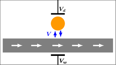
The quantum dot in Fig. 1 is side-coupled to a quantum wire. Current flows in response to a bias voltage applied to the wire. Gate potentials and control the dot occupation and the occupation of the Wannier orbital
| (1) |
where is the number of conduction states in the wire.
In standard notation, the Anderson Hamiltonian capturing the physics of this setup is
| (2) |
where the states form a structureless half-filled conduction band of halfwidth and density of states , the scattering potential is controlled by the gate voltage , and the tunneling amplitude couples the spin-degenerate dot level to the orbital.
It proves convenient to write the dot Hamiltonian in Eq. (2) in the form
| (3) |
which defines the antisymmetric component of the dot energy, i. e., the component that changes sign under the particle-hole transformation , . The second term on the right-hand side of the Eq. (3), by contrast, remains invariant under the same transformation. For , only the second term survives, and the Anderson Hamiltonian reduces to its symmetric form.Krishna-murthy et al. (1980b)
To highlight interference, many a study of transport through a nanodevice has explicitly introduced two conduction paths in the model Hamiltonian. The ratio between the amplitudes for charge transfer along the two routes, i. e., the Fano factor , is then a model parameter.
An alternative approach is possible. A sufficiently comprehensive model Hamiltonian may implicitly include two conduction routes and hence define an effective Fano factor .111Even if the Fano factor is defined with the model Hamiltonian, electronic correlations may renormalize it. An example was provided by L. N. Oliveira and J. W. Wilkins, Phys. Rev. B, 32, 696 (1985). Fano’s pioneer analysis of self-ionization in the He atom provided the first example of this approach,Fano (1961) which we adopt. A simple extension of Eq. (2) would provide another example.Seridonio et al. (2009) A momentum-dependent coupling between the quantum wire and the quantum dot would introduce a conduction path alternative to transport straight through the quantum wire and define an effective Fano factor proportional to the Fermi-level value of the derivative .Seridonio et al. (2009)
The momentum-independent coupling in Eq. (2) rules out this alternative route. Section IV will show, however, that the wire gate potential opens a bypass through the quantum dot, so that an effective Fano factor arises, which grows with . As long as , Eq. (2) comprises two conduction paths, through which currents can flow and interference.
To reproduce the model Hamiltonian in Ref. Seridonio et al., 2009, a momentum-dependent coupling could have been substituted for the third term on the right-hand side of Eq. (2). Any of a variety of artificial couplings between the dot and the wire orbitals orthogonal to might equally well have been introduced, to generate another bypass and originate a different Fano parameter. In any case, the results would be equivalent to those in Sec. IV, because the universal mapping between the temperature-dependent conductance and the function derived in Ref. Seridonio et al., 2009 depends only on the ground-state phase shift . Since decreases from to zero as the wire potential grows, our survey of the conductance for the structure in Fig. 1 samples well the dependence of the conductance on Fano factors. Alternative Hamiltonians would yield the same information.
II.2 Conductance
Reference Yoshida et al., 2009a derived an expression for the temperature-dependent electrical conductance in the embedded configuration. The same analysis leads to an analogous equality for the conductance in the side-coupled configuration:
| (4) |
where is the partition function, () is an eigenstate of , with eigenvalue (), and is the dot-level width, due to its coupling to the quantum wire.
To describe the temperature and dot-energy dependence of the conductance, it is sufficient to consider non-negative wire gate potentials. Since the model Hamiltonian and the conductance remain invariant under the modified particle-hole transformation
| (5) |
given two energies and , the conductance for and is given by the right-hand side of Eq. (4) for and . The conductance for a negative wire gate potential can therefore be obtained from the results for the symmetric (positive) potential.
II.3 Characteristic energy scales
Figure 3 in Ref. Yoshida et al., 2009a depicts the five characteristic energies in the spectrum of the Hamiltonian (2). The first (second), due to the dot Hamiltonian (3), is the excitation energy () necessary to remove an electron from (add an electron to) the singly-occupied level. The only scale in the conduction band Hamiltonian is trivial: the halfwidth . The coupling to the dot, on the other hand, makes two important contributions: the level width , and the Kondo energy . The scattering potential reduces the former to Yoshida et al. (2009a)
| (6) |
The Kondo regime is defined by the condition , where the dominant characteristic energy is . The and dot configurations are then energetically inaccessible, and a dot magnetic moment arises. As the temperature is reduced below the band halfwidth , the antiferromagnetic interaction between the conduction electrons and the dot electron progressively screens the moment. The energy of the resulting low-temperature singlet defines the fifth characteristic scale in our set: the Kondo energy .
A side effect of the coupling between the dot and the conduction electrons, one that emerges in the spectrum of particle-hole asymmetric Hamiltonians, is the renormalization , or , of the lowest dot-excitation energy.Haldane (1978); Krishna-murthy et al. (1980a) Although of no other practical consequence, this energy shift is important because it displaces both the Kondo and the mixed-valence regimes.Yoshida et al. (2009b)
The latter regime comprises the two regions in the parametric space of the model Hamiltonian that enclose the Kondo regime. One of them is defined by the inequality , the other, by . In the mixed-valence regime the dominant characteristic energy is , and at high temperatures, the dot moment is only partially formed. As the thermal energy is reduced past , the dot level couples strongly to the surrounding conduction electrons, and all physical properties approach their low-temperature limit.
III Universal mapping
The derivation of the universal expression mapping the conductance in Eq. (4) to the universal function computed by Costi, Hewson, and ZlaticCosti et al. (1994); Bulla et al. (2008) has been summarized elsewhere.Seridonio et al. (2009) A detailed presentation of the analogous derivation for the single-electron transistor being moreover available,Yoshida et al. (2009a) only recapitulation of the central result is required:
| (7) |
Here, is the ground-state phase shift of the conduction electrons in the wire.
To make the physical content of Eq. (7) more visible, we rewrite it in the equivalent form
| (8) |
which shows that the conductance is a linear combination of the universal function with its complement, . While the universal, monotonically decreasing function describes the conductance through a particle-hole symmetric quantum dot in the embedded configuration, is the monotonically increasing function that describes the conductance through a particle-hole symmetric quantum dot in the side-coupled configuration. For particle-hole asymmetric -shaped devices, the first term on the right-hand side of Eq. (8) describes the current through the bypass, while the second term accounts for the current traversing the wire. If the two conduction paths were independent, the resultant conductance would be the sum ; the coefficients and thus account for the interference between the two fluxes.
Special limits
| Four limits of Eq. (8) merit special attention. For , the mapping reduces to | |||
| (9a) | |||
The equality, which can be derived from a diagrammatic expansion for the symmetric Anderson Hamiltonian,Maruyama et al. (2004); Yoshida et al. (2009a) shows that, with , the conductances for the side-coupled and the embedded geometries are complementary. This result is particularly important because, in the absence of a wire gate potential, the Friedel sum ruleLangreth (1966) pins the ground-state phase shift to the vicinity of .Yoshida et al. (2009b) For , the conductance through the -shaped device is therefore expected to decay from nearly ballistic to nearly zero as the temperature rises.
In the second special limit, , Eq. (7) yields
| (9b) |
In the absence of a wire gate potential, the ground-state phase shift is close to ; a strong wire potential must be applied to make . The potential affects the conductance in two different ways: it induces a charge that blocks transport through the central region of the wire; at the same time, it opens a bypass through the quantum dot. At high temperatures, the Coulomb blockade against conduction through the dot makes the bypass ineffective, so that the conductance of the device vanishes. Upon cooling, however, the Kondo effect raises the blockade and the conductance rises, lifted by the very same mechanism that allows conduction through a single-electron transistor.Glazman and Raikh (1987); Ng and Lee (1988); Goldhaber-Gordon et al. (1998a) In brief, Eq. (9b) tells us that a strong wire potential diverts the current to the bypass and makes the -shaped device emulate a single-electron transistor.
The third simple limit of Eq. (7) is . At low temperatures, the universal curve approaches . From Eq. (7), it follows that
| (9c) |
a result that can be derived from an extension of Langreth’s argumentLangreth (1966) relating the low-energy dot-level spectral density to the ground-state phase shift.Seridonio et al. (2009)
Finally, at high temperatures, the universal function vanishes, and Eq. (7) yields
| (9d) |
Analogous to Eq. (9c), this result also stems from Langreth’s expression. In the temperature range , within the Kondo regime, the Anderson Hamiltonian is in the local-moment regime, equivalent to a phase shifted conduction band weakly interacting with the dot moment.Krishna-murthy et al. (1980b) The interaction neglected, the Hamiltonian reduces to a free conduction band, to which Langreth’s reasoning applies.Seridonio et al. (2009); Yoshida et al. (2009a) The phase shift of the wire electrons can be obtained from the Friedel sum rule, which associates a phase-shift difference with the Kondo cloud. We hence have that , and so . Substitution of for in Eq. (9c) leads to Eq. (9d).
IV Numerical results
We are now ready to discuss the NRG results and compare them with Eq. (7). A previous report detailed the numerical procedure yielding the ground-state phase shift , and the temperature-dependent conductance and tabulated the parameters controlling the accuracy of the computation.Yoshida et al. (2009b) Here, to follow the structure of that paper, we will discuss before examining .
IV.1 Phase shifts
Figure 2 shows the ground-state phase shift, extracted from the low-energy spectrum of the Hamiltonian , as a function of the dot-energy in the interval , i. e., for . It follows from the Friedel sum rule that the ordinate is the extra charge piled up at the wire. That accumulation is the sum of two charges: the charge induced by the wire potential, the absolute value of which grow with ; and the Kondo screening charge, which is equal to the dot occupation and hence close to unity in the Kondo regime.
With no wire potential, the charges and coincide. If , then reduces to the symmetric Hamiltonian, the dot occupation is unitary, and . If, on the other hand, , then a particle-hole transformation, which reverses the sign of , transmutes into and hence changes the sign of . The curve through the circles in Fig. 2 thus remains invariant under a rotation of 1800 around the point , .
The solid line through the circles marks the Kondo regime, throughout which . Comparison with the solid lines through the squares and triangles shows that the positive gate potential applied to the wires displaces the Kondo regime to higher dot energies.
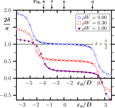
The negative charge induced by the potential pushes down the phase shifts and spoils the symmetry about , . In the region , the wire charge can now become negative. While the circles cross the line at a saddle point, the slope of the curves through the squares and triangles is markedly negative. Thus, in contrast with the circles, only in narrow ranges of dot energies do the squares and triangles dwell near or . As the data moreover show, except for , the range in which ( is pinned to the vicinity of the mixed-valence region ().
Combined with Eq. (7), the information in Fig. 2 determines the thermal dependence of the conductance through the device in Fig. 1. Detailed comparison between the resulting curves and the NRG conductances will be presented in Secs. IV.1-IV.4. Before that, to provide a more visual description of the numerical data, we present bird’s-eye views of the conductance as a function of the temperature and dot-level energy.
IV.2 Conductance for
Figure 3 is a landscape consolidating 71 curves calculated for , , , and dot energies in the range displayed in Fig. 2. The inset is a reversed-perspective view of the same plot offering an unobstructed depiction of the low-temperature region.
Eqs. (9a)-(9d) explain the salient features of the landscape. The central portion of the plot encompasses the Kondo regime. Here, as the circles in Fig. 2 show, the ground-state phase shift is close to . At high temperatures, Eq. (9d) yields the nearly ballistic conductance depicted by the hood-like central plateau visible in the main plot and inset. At low temperatures, Eq. (9c) brings the conductance down to nearly zero; the resulting Kondo valley can be seen in the inset.
We defer to Sec. IV.5.1 the quantitative discussion of the crossover between the plateau and the valley. Here, we note that the Kondo temperature rises with . For , in particular, i. e., for or , the Kondo temperature becomes comparable with , an indication that the Hamiltonian has transposed the limits of the Kondo domain to enter the mixed-valence regime.
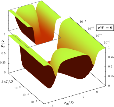
At high temperatures, the mixed-valence regime is identified by the two antiresonances bringing the conductance to on the frontal plane in the main plot, or the rear plane in the inset. As the temperature is reduced, the conductance descends into the Kondo valley. As Sec. IV.2 will show, the decay can still be mapped onto the universal function . Given the high crossover temperature, however, only the low-temperature tail of the numerical results agrees quantitatively with (7).
Beyond the mixed-valence regime, as grows past , the dot occupation approaches an even integer, or , the coupling to the quantum wire becomes ineffective, and the electrons flow ballistically accross the wire.
IV.3 Conductance for weak scattering potentials
Even moderate gate potentials applied to the wire change qualitatively the conductance landscape. Figure 4 shows plots analogous to Fig. 3, calculated for the same Coulomb repulsion and effective dot-level width , and for three weak potentials: (a) ; (b) ; and (c) . Compared to the symmetric landscape in Fig. 3, the new plots show distinctions that evolve rapidly under the rising gate potential.
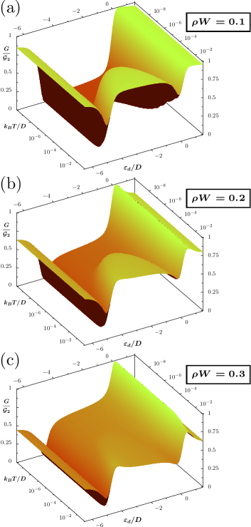
The Kondo-valley conductance rises with , while the high-temperature plateau diminishes. For the highest potential shown, , the Kondo-regime conductance is nearly uniform. Outside the Kondo regime, in the even- regions, the charge induced by the wire potential lowers the ground-state phase shift to () in the () domain. The right-hand side of Eq. (9c) is no longer ballistic: .
In the mixed-valence regime, the transition from the Kondo regime to the domain is now markedly different from the transition to the domain. The former encompasses the narrow dot-energy range in Fig. 2, for which the right-hand side of Eq. (9c) yields ; while the latter traverses the equally narrow range, for which Eq. (9c) yields . An insulating ravine develops in the conductance landscape, pinned near , while a ballistic ridge arises near the plane. Plotted at fixed temperature against the dot energy, the conductance displays the trough-crest pair that defines a Fano profile.Fano (1961) As evidenced by Fig. 4(c), this fiducial mark of interference between currents flowing along parallel paths becomes most pronounced for intermediate wire potentials.
A brief glance at Fig. 1 identifies the interfering fluxes. One of them, indicated by the white arrows, is subject to obstruction by the charge accumulated in the central segment of the wire. The second conduction path runs through the quantum dot. To provide an effective bypass, it must avoid the Wannier orbital . At first sight, given that Eq. (2) couples the quantum dot to , this may seem impossible, and in fact it is, for . The wire potential nonetheless spreads the coupling over wire states beyond the central orbital closest to the dot.
To be more specific, we let and consider the resulting wire Hamiltonian,
| (10) |
The diagonalization of this quadratic form yieldsYoshida et al. (2009a)
| (11) |
where
| (12) |
with coefficients that depend on . The eigenvalues are phase-shifted with respect to the . In the vicinity of the Fermi level, in particular, the phase shifts are uniform:Krishna-murthy et al. (1980a); Yoshida et al. (2009a)
| (13) |
In analogy with Eq. (1), we can therefore define
| (14) |
A straightforward calculation shows that .Yoshida et al. (2009a) For , in particular, . It is also easy to check that the ground-state occupation of the orbital is , so that as required by the Friedel sum rule, the gate potential brings in an extra charge .
The operator plays the role that belonged to when . In the Kondo regime, the antiferromagnetic interaction between the dot moment and the moment of the electrons occupying the orbital is now responsible for the Kondo crossover,Krishna-murthy et al. (1980a); Yoshida et al. (2009a) and at low temperatures, the occupation, equal to the charge in the Kondo cloud plus that induced by the wire potential, obstructs the transport along the white arrows in Fig. 1. At the same time, the overlap between and the wire states orthogonal to offers the dot bypass, through which the current runs to interfere with the flow across and generate the askew profile most visible on the plane (i. e., the rear plane) in Fig. 4(c).
The amplitude for tunneling through the dot is . The amplitude for tunneling accross the orbital is . The ratio between the two amplitudes defines the effective Fano parameter
| (15) |
IV.4 Conductance for strong scattering potentials
Under stronger gate potentials, while the amplitude for conduction along the white arrows in Fig. 1 diminishes, the dot bypass becomes more effective. The absolute value of the right-hand side of Eq. (15) grows, and the conductance profile at low temperatures gradually acquires the symmetry of the large- Fano profile.
Illustrative landscapes are displayed in Figs. 5(a), (b), and (c), computed for , 0.6, and 1.0, respectively, and and . The dominant features of Fig. 4 reappear in the three plots. In particular, the ballistic ridge and the insulating ravine are still clearly visible in the mixed-valence regime. Sharp in (a) and (b) the Fano antiresonance becomes dull in Fig. 5(c), because as shown by the triangles in Fig. 2, the wire potential pushes so far down that the phase-shift curve crosses the horizontal lines at the and with relatively small slopes.
In the Kondo regime, while the high-temperature conductance falls, the low-temperature conductances rises steadily with . In the end, with , the conductance is nearly ballistic in the low-temperature Kondo plateau, while at high temperatures the Coulomb blockade (the charge induced by the wire potential) impedes transport through the dot (through the wire) and reduces the conductance to nearly zero.
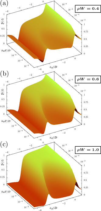
The trend in Fig. 5 indicates that, in the large limit, the conductance landscape is complementary to the plot in Fig. 3, i. e., . In view of Eq. (9a), we expect to reproduce the thermal-dependence of the conductance for a single-electron transistor.Yoshida et al. (2009a, b) Comparison with Fig. 4 in Ref. Yoshida et al., 2009b, which describes a single-electron transistor with the same model parameters, confirms that, with , the conductances in the side-coupled and the embedded configurations are identical.
For , instead of equal, the conductancesa are complementary. While the conductance for the -shaped device displays the Kondo-valley profile in Fig. 3, the conductance through the single-electron transistor, which is insensitive to changes in the wire gate potential, retains the Kondo-plateau pattern to which the trend in Figs. 5(a)-(c) points.
IV.5 Thermal dependence of the conductance
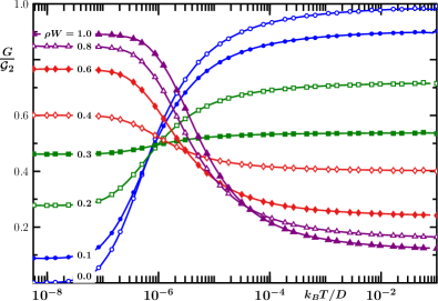
This section compares the NRG results for the temperature dependence of the conductance with the mapping (7). We fix the parameters and , and consider the eight gate wire potentials in Table 1. To sample the dot-energy dependence of the data, four plots will be discussed, correspondig to the four dot energies indexed by the vertical arrows in Fig. 2. For each run, the table shows the Kondo temperature resulting from the definition and the ground-state phase shift calculated from the low-energy eigenvalues of .Yoshida et al. (2009b)
| Figure | Symbol | Symbol | ||||||
|---|---|---|---|---|---|---|---|---|
| 6 | 0.00 | 0.50 | 8.1 | 0.10 | 0.40 | 8.6 | ||
| 6 | 0.20 | 0.32 | 1.0 | 0.30 | 0.26 | 1.3 | ||
| 6 | 0.40 | 0.22 | 1.6 | 0.60 | 0.16 | 2.5 | ||
| 6 | 0.80 | 0.13 | 3.8 | 1.00 | 0.11 | 6.0 | ||
| 7 | 0.00 | 0.51 | 4.4 | 0.10 | 0.41 | 5.9 | ||
| 7 | 0.20 | 0.33 | 8.9 | 0.30 | 0.27 | 1.4 | ||
| 7 | 0.40 | 0.23 | 2.2 | 0.60 | 0.17 | 5.7 | ||
| 7 | 0.80 | 0.15 | 1.4 | 1.00 | 0.13 | 3.6 | ||
| 8 | 0.00 | 0.52 | 8.8 | 0.10 | 0.43 | 1.4 | ||
| 8 | 0.20 | 0.35 | 2.5 | 0.30 | 0.29 | 4.5 | ||
| 8 | 0.40 | 0.25 | 9.6 | 0.60 | 0.22 | 3.0 | ||
| 8 | 0.80 | 0.22 | 1.0∗ | 1.00 | 0.25 | 1.2∗ | ||
| 9 | 0.00 | 0.42 | 8.0 | 0.10 | 0.34 | 4.5 | ||
| 9 | 0.20 | 0.27 | 2.7 | 0.30 | 0.21 | 2.0 | ||
| 9 | 0.40 | 0.17 | 1.4 | 0.60 | 0.12 | 6.6 | ||
| 9 | 0.80 | 0.09 | 3.5 | 1.00 | 0.08 | 1.9 |
IV.5.1 Symmetric dot Hamiltonian
Figure 6 shows the thermal dependence of the conductance for and the eight gate potentials in Table 1. As the potential grows from to , the ground-state phase shift decreases from to nearly zero, and the conductance evolves from monotonically increasing to monotonically decreasing. In all cases, the model Hamiltonian lying well within the Kondo regime, the agreement with the solid curves representing Eq. (7) is excellent.
IV.5.2 Asymmetric models
Figure 7 displays temperature-dependent conductances for , equivalent to . The other model parameters coincide with those in Fig. 6. As Table 1 shows, the enhanced particle-hole asymmetry makes each ground-state phase shift somewhat larger than the corresponding in Fig. 6. For (open circles) the phase shift in Fig. 6 was , so that the factor on the right-hand side of Eq. (7) is now larger than it was. The more negative dot energy thus flattens the conductance curve.
For each nonzero potentials, the phase shift associated with Fig. 7 in Table 1 makes the factor smaller than the corresponding factor in Fig. 6. Equation (9c) therefore pushes down the low-temperature conductances, while Eq. (9d) pushes up the high-temperature conductances. The Kondo temperatures are now spread over a wider ranger. Apart from such minor changes, however, Figs. 6 and 7 display the same picture. In particular, all Hamiltonians and temperatures being in the Kondo regime, the numerical conductances are in very good agreement with Eq. (7).
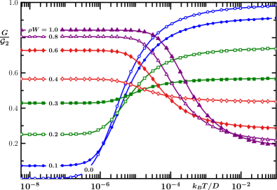
More negative dot energies can displace the Hamiltonian into the mixed-valence regime. As indicated by the solid lines in Fig. 2, for the Kondo domain extends from to ; with , i. e., , the model is still within it. As grows, however, the Kondo regime is uniformly shifted toward higer dot energies. It results that the open and filled triangles in Fig. 8, which describe conductances for and 1, respectively, represent Hamiltonians in the mixed-valence regime.
While the other curves, computed for smaller ’s, agree with Eq. (7), the deviations separating the triangles from the solid lines at high temperatures, , are substantial. The discrepancies are reminders that, in the mixed-valence regime, the dominant characteristic energy is , which restricts the domain of Eq. (7) to . Our numerical study of the embedded configuration reported similar deviations.Yoshida et al. (2009b)
Since the conductance curves for large cross the horizontal at relatively high temperatures, which fall in the nonuniversal thermal range , it would be inappropriate to extract Kondo temperatures from the identification . To evaluate each of the two numbers marked with asterisks in Table 1, we therefore adjusted so that the corresponding solid line ran through the triangle closest to .
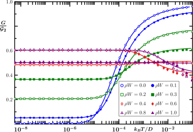
Since the wire potential displaces the Kondo regime to higher dot energies, for we expect the Hamiltonian to leave the Kondo regime before the Hamiltonians. Accordingly, Fig. 9 contrasts triangles and squares very well fitted by Eq. (7) with circles and diamonds that depart significantly from the solid lines representing the universal mapping for .
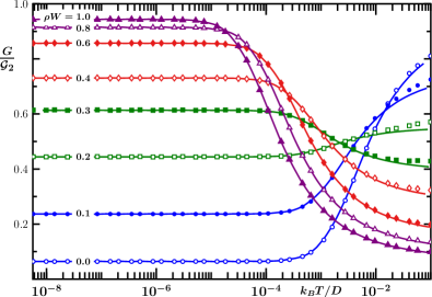
The ground-state phase shift decreases with . Thus, while the phase shift for each curve in Figs. 7 and 8 exceeds the phase shift for the same in Fig. 6, the phase shift for each curve in Fig. 9 is smaller than the corresponding phase shift in Fig. 6. In compliance with Eq. (9c), the low temperature conductances in Fig. 9 are higher than the corresponding in Fig. 8. At high temperatures, the analogous comparison is unproductive, because the relatively high Kondo temperatures place the high-temperature end of the axis in Fig. 9 outside the reach of Eq. (9d).
IV.6 Comparison with experiment
The numerical results in Figs. 3-5 can be compared to a number of experimental studies of transport in -shaped devices.Kobayashi et al. (2004); Sato et al. (2005); Katsumoto et al. (2006); Aharony et al. (2006); Otsuka et al. (2007); Katsumoto (2007) Particularly illustrative are Fig. 1(c) in Ref. Sato et al., 2005, and Fig. 5 in Ref. Katsumoto et al., 2006. The former, which shows low-temperature conductance profiles for various level widths, exhibits valleys, plateaus, and antiresonances—all the conspicuous features in the conductance profiles at in Figs. 3-5.
Even more instructive is the illustration in Ref. Katsumoto et al., 2006, which demonstrates that the wire gate potential controls the division of the current between the wire and the bypass. The evolution of the low-temperature conductance profile under an increasing wire gate potential is documented in the plot. The profile starts out as Kondo valley analogous to the low-temperature profile in Fig. 3. It then evolves to a curve marked by interference, analogous to the low-temperature profile in Fig. 4(c). Finally, it reaches a Kondo plateau, analogous to the low-temperature profile in Fig. 5(c). The NRG results and Eq. (7) are therefore in qualitative agreement with the experimental results.
What is more important, the mapping describes quantitatively the thermal dependence of measured conductances. A fit of the temperature-dependent conductances resulting from two gate potentials applied by Sato et al.Sato et al. (2005) to a -shaped device was presented in Ref. Seridonio et al., 2009. A background current being detected, three parameters were involved in the fit to the first conductance curve: the background conductance, the phase shift, and the Kondo temperature . The same first two parameters and a different Kondo temperature then fitted the second curve. In each case, within the dispersion of the experimental data, optimum agreement resulted.
V Conclusions
Equation (7) offers a unifying view of electrical conduction through a quantum wire side-coupled to a quantum dot. Valid over the entire Kondo regime, it captures with error the conductance crossover from the local-moment regime (i. e., high-temperatures, ), equivalent to a conduction band weakly interacting with the dot magnetic moment, to the low-temperature regime (), in which the dot electron and the conduction electrons around it lock into a singlet that reduces the model Hamiltonian to a phase-shifted conduction band.
The phase shift controls the thermal dependence of the conductance. With no wire gate potential, the Friedel makes , and the Kondo cloud lowers the conductance from nearly ballistic at high to nearly zero at low . For , the conductances for the -shaped device and the single-electron transistor are complementary.Yoshida et al. (2009b)
A (positive) gate potential applied to the wire in the -shaped device induces electric charge that reduces the ground-state phase shift. As pushes below , the conductance curve first becomes flat and then reverses the pattern in Fig. 3. For large , as indicated by Fig. 5(c), the conductance through the -shaped device approaches the conductance through a single-electron transistor.Yoshida et al. (2009b)
The Friedel sum rule explains why the two devices respond differently to the wire gate potential. In the embedded configuration, since the dot is in the conduction path, its occupation controls the conductance. Although the wire gate potential determines the amount of charge in the wire, it has little influence upon : according to the Friedel sum rule, , so that the charge induced by the gate potential is subtracted from the total charge piled up in the quantum wire. We therefore expect the conductance through the single-electron transistor to be independent of . The mapping between and the universal function , which is parametrized by the phase-shift difference , ractifies this reasoning.Yoshida et al. (2009a, b)
By contrast, the mapping between the conductance through the device in Fig. 1 and the universal function is parametrized by the phase shift . According to the Friedel sum rule, the wire charge is . Much as the dot charge , which controls conduction in the embedded configuration, parametrizes the mapping to the conductance through the single-electron transistor,Yoshida et al. (2009a) the wire charge controls conduction in the side-coupled configuration and parametrizes the mapping (7). While the dependence on the dot charge practically shields the single-electron transistor from gate potentials applied to the wire, the dependence on the wire charge makes the conductance through the -shaped device remarkably sensitive to such potentials.
The wire gate potential affects Fig. 1 in two ways. First, the total charge in the orbital, equal to the charge induced by the wire potential plus, at low temperatures, the charge in the Kondo droplet, obstructs transport through the central portion of the wire. Second, the potential couples to states orthogonal to and thus opens a bypass through the quantum dot. For very weak (strong) potentials, the path through () is dominant; the landscape in Fig. 3 [ 5(c)] is thus complementary (very similar) to the landscape for a single-electron transistor.Yoshida et al. (2009b)
For intermediate potentials [Fig. 4(c)], the interference between the currents along the two paths makes the landscape markedly asymmetric in the mixed-valence region. At the same time, in the Kondo regime, the two parallel conduction paths, one efficient at low temperatures, the other efficient at high temperatures, make the landscape remarkably flat.
The practical value of universality has been demonstrated in both experimental arrangements. In the embedded configuration, early in the history of the single-electron transistor, the universal function guided the interpretation of conductance data.Goldhaber-Gordon et al. (1998b) In the side-coupled arrangement, Eq. (7) was shown to fit conductance curves generated in the laboratorySato et al. (2005); Katsumoto et al. (2006) accurately enough to determine the Kondo temperature and ground-state phase shift within deviations set by the dispersion of the experimental data.Seridonio et al. (2009)
Neither the universal mapping (7), nor the corresponding expression for the embedded configurationYoshida et al. (2009a) determine explicitly any of the model parameters, let alone the physical constants emulated by the model Hamiltonian. They offer indirect information that may assist future ab initio descriptions of the physical properties of single-electron transistors or -shaped devices. The two mappings of the Kondo-regime conductances to the universal function redefine the ultimate target of such ab initio problems, from the computation of conductance curves to the computation of phase shifts and Kondo temperatures. In a less challenging arena, the mappings bring Kondo-regime conductance curves within the reach of the Bethe-ansatz approach.Andrei et al. (1983); Tsvelick and Wiegmann (1983) Finally, on the basis of the experience with thermodynamical properties,Silva et al. (1996); Campo Jr and Oliveira (2004) we expect the mappings to offer benchmarks to check the accuracy of numerically or analytically computed transport properties for model Hamiltonians describing quantum-dot arrays.
Acknowledgements.
One of us (LNO) thanks the hospitality at the Institut Henri Poincaré (Paris), where this research was started. This work was supported by the CNPq and FAPESP.References
- Hofstetter et al. (2001) W. Hofstetter, J. König, and H. Schoeller, Phys. Rev. Lett. 87, 156803 (2001).
- Aikawa et al. (2004) H. Aikawa, K. Kobayashi, A. Sano, S. Katsumoto, and Y. Iye, Phys. Rev. Lett. 92, 176802 (pages 4) (2004), URL http://link.aps.org/abstract/PRL/v92/e176802.
- Aharony et al. (2006) A. Aharony, O. Entin-Wohlman, T. Otsuka, S. Katsumoto, H. Aikawa, and K. Kobayashi, Phys. Rev. B 73, 195329 (pages 8) (2006).
- Fuhrer et al. (2006) A. Fuhrer, P. Brusheim, T. Ihn, M. Sigrist, K. Ensslin, W. Wegscheider, and M. Bichler, Phys. Rev. B 73, 205326 (pages 9) (2006).
- Dias da Silva et al. (2006) L. G. G. V. Dias da Silva, N. P. Sandler, K. Ingersent, and S. E. Ulloa, Phys. Rev. Lett. 97, 096603 (pages 4) (2006).
- Maruyama et al. (2004) I. Maruyama, N. Shibata, and K. Ueda, J. Phys. Soc. Japan 73, 3239 (2004).
- Sato et al. (2005) M. Sato, H. Aikawa, K. Kobayashi, S. Katsumoto, and Y. Iye, Phys. Rev. Lett. 95, 066801 (2005).
- Kobayashi et al. (2004) K. Kobayashi, H. Aikawa, A. Sano, S. Katsumoto, and Y. Iye, Phys. Rev. B 70, 035319 (2004).
- Katsumoto (2007) S. Katsumoto, J. Phys.: Condens. Matter 19, 233201 (2007).
- Bulka and Stefanski (2001) B. R. Bulka and P. Stefanski, Phys. Rev. Lett. 86, 5128 (2001).
- Clerk et al. (2001) A. A. Clerk, X. Waintal, and P. W. Brouwer, Phys. Rev. Lett. 86, 4636 (2001).
- Torio et al. (2002) M. E. Torio, K. Hallberg, A. H. Ceccatto, and C. R. Proetto, Phys. Rev. B 65, 085302 (2002).
- Franco et al. (2003) R. Franco, M. S. Figueira, and E. V. Anda, Phys. Rev. B 67, 155301 (2003).
- Zitko and Bonca (2006) R. Zitko and J. Bonca, Phys. Rev. B 73, 035332 (2006).
- Maruyama et al. (2006) I. Maruyama, N. Shibata, and K. Ueda, Physica B 378-380, 938 (2006).
- Hewson (1993) A. C. Hewson, The Kondo Problem to Heavy Fermions (Cambridge University Press, Cambridge, 1993).
- Costi et al. (1994) T. Costi, A. Hewson, and V. Zlatic, Journal of Physics–Condensed Matter 6, 2519 (1994).
- Anderson (1961) P. W. Anderson, Phys. Rev. 124, 41 (1961).
- Yoshida et al. (2009a) M. Yoshida, A. C. Seridonio, and L. N. Oliveira, Universal zero-bias conductance for the single-electron transistor (2009a), URL arXiv:0906.4063.
- Katsumoto et al. (2006) S. Katsumoto, M. Sato, H. Aikawa, and Y. Iye, Physica E: Low-dimensional Systems and Nanostructures 34, 36 (2006).
- Otsuka et al. (2007) T. Otsuka, E. Abe, S. Katsumoto, Y. Iye, G. L. Khym, and K. Kang, J. Phys. Soc. Japan 76, 084706 (2007).
- Dias da Silva et al. (2008) L. G. G. V. Dias da Silva, K. Ingersent, N. Sandler, and S. E. Ulloa, Phys. Rev. B 78, 153304 (2008).
- Seridonio et al. (2009) A. C. Seridonio, M. Yoshida, and L. N. Oliveira, Europhys. Lett. 86, 67006 (2009).
- Yoshida et al. (2009b) M. Yoshida, A. C. Seridonio, and L. N. Oliveira, Universal zero-bias conductance for the single-electron transistor. ii: Numerical results (2009b), URL arXiv:0906.4228.
- Haldane (1978) F. D. M. Haldane, Phys. Rev. Lett. 40, 416 (1978).
- Krishna-murthy et al. (1980a) H. R. Krishna-murthy, J. W. Wilkins, and K. G. Wilson, Phys. Rev. B 21, 1044 (1980a).
- Krishna-murthy et al. (1980b) H. R. Krishna-murthy, J. W. Wilkins, and K. G. Wilson, Phys. Rev. B 21, 1003 (1980b).
- Fano (1961) U. Fano, Phys. Rev. 124, 1866 (1961).
- Bulla et al. (2008) R. Bulla, T. A. Costi, and T. Pruschke, Rev. Mod. Phys. 80, 395 (2008), ISSN 0034-6861.
- Langreth (1966) D. C. Langreth, Phys. Rev. 150, 516 (1966).
- Goldhaber-Gordon et al. (1998a) D. Goldhaber-Gordon, H. Shtrikman, D. Mahalu, D. Abusch-Magder, U. Meirav, and M. A. Kastner, Nature 391, 156 (1998a).
- Glazman and Raikh (1987) L. I. Glazman and M. E. Raikh, JETP Lett. 47, 452 (1987).
- Ng and Lee (1988) T. K. Ng and P. A. Lee, Phys. Rev. Lett. 61, 1768 (1988).
- Goldhaber-Gordon et al. (1998b) D. Goldhaber-Gordon, J. Göres, M. A. Kastner, H. Shtrikman, D. Mahalu, and U. Meirav, Phys. Rev. Lett. 81, 5225 (1998b).
- Andrei et al. (1983) N. Andrei, K. Furuya, and J. H. Lowenstein, Rev. Mod. Phys. 55, 331 (1983).
- Tsvelick and Wiegmann (1983) A. M. Tsvelick and P. B. Wiegmann, Advances in Physics 32, 453 (1983).
- Silva et al. (1996) J. B. Silva, W. L. C. Lima, W. C. Oliveira, J. L. N. Mello, L. N. Oliveira, and J. W. Wilkins, Phys. Rev. Lett. 76, 275 (1996).
- Campo Jr and Oliveira (2004) V. L. Campo Jr and L. N. Oliveira, Phys. Rev. B 70, 153401 (2004).