A First-Principles Study of Zinc Oxide Honeycomb Structures
Abstract
We present a first-principles study of the atomic, electronic and magnetic properties of two dimensional (2D), single and bilayer ZnO in honeycomb structure and its armchair and zigzag nanoribbons. In order to reveal the dimensionality effects, our study includes also bulk ZnO in wurtzite, zincblende and hexagonal structures. The stability of 2D ZnO, its nanoribbons and flakes are analyzed by phonon frequency, as well as by finite temperature ab-initio molecular dynamics calculations. 2D ZnO in honeycomb structure and its armchair nanoribbons are nonmagnetic semiconductors, but acquire net magnetic moment upon the creation of zinc vacancy defect. Zigzag ZnO nanoribbons are ferromagnetic metals with spins localized at the oxygen atoms at the edges and have high spin polarization at the Fermi level. However, they change to nonmagnetic metal upon termination of their edges with hydrogen atoms. From the phonon calculations, the fourth acoustical mode specified as twisting mode is also revealed for armchair nanoribbon. Under tensile stress the nanoribbons are deformed elastically maintaining honeycomb like structure, but yield at high strains. Beyond yielding point honeycomb like structure undergo a structural change and deform plastically by forming large polygons. The variation of the electronic and magnetic properties of these nanoribbons have been examined under strain. It appears that plastically deformed nanoribbons may offer a new class of materials with diverse properties.
pacs:
73.22.-f, 75.75.+a, 63.22.-mI introduction
Graphene, a monolayer layer of carbon atoms in honeycomb structure, is offering exceptional propertiesnovo ; zhang ; berger which may lead to important applications in various fields. Normally, two dimensional (2D) graphene is semimetallic and its electrons and holes behave like a massless Dirac fermion. Whereas 2D boron-nitride (BN),bn-synthesis_bn-insulator Group III-V analogue of graphene, in ionic honeycomb structure is a wide band gap semiconductor. Unusual properties of graphene and BN nanoribbons have been revealed extensively in recent papers.gribbon1 ; gribbon2 ; gribbon3 ; gribbon4 ; bnribbon1 ; bnribbon2 ; bnribbon3 More recently, based on state-of-the art first principles calculations it was predicted that Si and Geseymur , even binary compounds of Group IV elements and III-V compoundshasan can form 2D stable monolayer honeycomb structures. Earlier studies on ZnO and its nanowires gave first indications that graphitic ZnO can exists.claeyssens ; kulkarni Very thin nanosheets,nanosheet nanobelts,nanobelt nanotubesnanotube and nanowiresnanowire of ZnO have already been synthesized. Two monolayer thick ZnO(0001) films grown on Ag(111) were reported.bilayer
Because of its wide band gap of 3.3 eV and large exciton binding energy of 60 meV leading to vast optoelectronic applications including light-emitting diodes and solar cells,diode ; solar-cell ZnO has been the subject of various researches. It was reported that the vacancy defects can be intentionally created by electron irradiation method.annihilation It has been also reported that Zn vacancy induces ferromagnetism in ZnO thin films and nanowires without any need of doping with transition-metal atoms.jena These magnetic properties might provide superior advantages in biomedical applications because of non-toxic nature of ZnO as opposed to transition metal ions.
In this paper a comprehensive study of the atomic, electronic and magnetic properties of monolayer, bilayer and nanoribbons of II-VI ionic ZnO compound in honeycomb structures are carried out using first-principles calculations. In order to reveal the dimensionality effects, we started with the energetics and electronic energy bands of ZnO in different 3D bulk crystalline structures and compared them with those of 2D ZnO honeycomb structure. Our analysis based on phonon dispersions and finite temperature ab-initio molecular dynamics calculations provides evidence for the stability of free-standing 2D monolayer, bilayer and quasi 1D nanoribbons of ZnO honeycomb structures. These structures can be in different local minima on the Born-Oppenheimer surface, in spite of the fact that they are not synthesized yet. We found that 2D monolayer and bilayer ZnO are nonmagnetic semiconductors, but attain magnetic properties upon creation of Zn-vacancy defect. ZnO nanoribbons exhibit interesting electronic and magnetic properties depending on their orientation. While armchair ZnO nanoribbons are nonmagnetic semiconductors with band gaps varying with their widths, bare zigzag nanoribbons are ferromagnetic metals. These electronic and magnetic properties show dramatic changes under elastic and plastic deformation. Hence, ZnO nanoribbons can be functionalized by plastic deformation. Results obtained in this study indicates that 2D monolayer and bilayer ZnO honeycomb structures and quasi 1D armchair and zigzag nanoribbons display unusual electronic, magnetic and mechanical properties, which hold the promise of interesting technological applications.
II Model and Methodology
We have performed first-principles plane wave calculations within Density Functional Theory (DFT) using PAW potentials.paw The exchange correlation potential has been approximated by Generalized Gradient Approximation (GGA) using PW91 pw91 functional both for spin-polarized and spin-unpolarized cases. Recently, spin-polarized calculations within DFT have been used successfully to investigate magnetic properties of vacancy defects in 2D honeycomb structures. Also interesting spintronic properties of nanoribbons have been revealed using spin-polarized DFT.gribbon2 The success of spin-polarized DFT calculations has been discussed in Refzeller, .
All structures have been treated within supercell geometry using the periodic boundary conditions. A plane-wave basis set with kinetic energy cutoff of 500 eV has been used. The interaction between ZnO monolayers in adjacent supercells is examined as a function of their spacing. Since the total energy per cell has changed less than 1 meV upon increasing the spacing from 10 Å to 15 Å , we used the spacing of Å in the calculations. In the self-consistent potential and total energy calculations the Brillouin zone (BZ) is sampled by, respectively (15x15x15), (25x25x1) and (25x1x1) special k-points for 3D bulk, 2D honeycomb and 1D (nanoribbons) ZnO. This sampling is scaled according to the size of superlattices. For example, BZ was sampled by (331) special k-points for defect calculations using (77) supercell of 2D ZnO honeycomb structure. All atomic positions and lattice constants are optimized by using the conjugate gradient method, where the total energy and atomic forces are minimized. The convergence for energy is chosen as 10-5 eV between two steps, and the maximum Hellmann-Feynman forces acting on each atom is less than 0.02 eV/Å upon ionic relaxation. The pseudopotentials having 12 and 6 valence electrons for the Zn (Zn: ) and O ions (O: ) are used. Numerical plane wave calculations are performed by using VASP package.vasp1 ; vasp2 While all numerical calculations of structure optimization, electronic energy and phonon dispersions are carried out within GGA using VASP,vasp1 ; vasp2 some of the calculations are checked also by using PWSCFpwscf and SIESTAsiesta softwares. Therefore all pertaining discussions are based on the results obtained by using VASP software unless it is stated otherwise.
Since DFT within GGA underestimates the band gap, frequency-dependent GW0 calculations are carried out.gw Screened Coulomb potential, W, is kept fixed to initial DFT value W0 and Green’s function, G, is iterated five times. Various tests regarding vacuum separation, kinetic energy cut-off potential, number of bands, k-points and grid points are made. Final results of GW0 corrections are obtained using (12121) k-points in BZ, Å vacuum separation, 400 eV cut-off potential, 160 bands and 64 grid points. In addition to GW0, we performed also GW calculations in order to make comparison with earlier available studies. While GW0 corrections are successfully applied to 3D and 2D ZnO, its application to quasi 1D nanoribbons is hindered by large number of atoms.
III 3D bulk and 2D honeycomb ZnO crystal
We first consider 3D bulk ZnO, which are in wurtzite (wz-ZnO), zincblende (zb-ZnO) and hexagonal (h-ZnO, or graphite-like) crystals. Atoms in wz- and zb-ZnO structures are four fold coordinated through tetrahedrally directed -orbitals, whereas the atoms in h-ZnO crystal are three fold coordinated through -orbitals. Wurtzite structure is found to be the thermodynamically most stable phase of ZnO. The cohesive energy per Zn-O pair is calculated by using the expression,
| (1) |
in terms of the total energy of the optimized crystal structure of ZnO, per Zn-O pair, the total energies of free Zn and O atoms and . The equilibrium cohesive energies of wz-ZnO, zb-ZnO and h-ZnO structures are found to be 8.934, 8.919 and 8.802 eV per Zn-O pair, respectively. For wz-ZnO crystal, the hexagonal lattice constants of the optimized structure in equilibrium are Å, . The deviation of from the ideal value of 1.633 imposes a slight anisotropy in the lengths of tetrahedrally directed Zn-O bonds. While the length of three short bonds is 2.001 Å, the fourth bond is slightly longer and has the length of 2.007 Å. The zincblende structure in symmetry has cubic lattice constant Å and four tetrahedrally coordinated Zn-O bonds having uniform length, Å . The h-ZnO structure has hexagonal lattice constants Å, and . The structural parameters of these three bulk ZnO crystals are shown in Fig. 1. The lattice constant of wz-ZnO, () is measured between 3.247 (1.6035) Å and 3.250 (1.602) Å using different methods.bulk_zno The calculations based on ab-initio LCAO method with all-electron Gaussian type basis set predict =3.286 Å and =1.595.allelect All our results related with the structural parameters are in good agreement with the experimental and theoretical values within the average error of 1 %.bulk_zno ; allelect
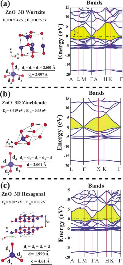
The optimized atomic structure and corresponding electronic band structure of 3D ZnO crystals are presented in Fig. 1. All wz-ZnO, zb-ZnO and h-ZnO crystals are direct band gap semiconductors with calculated band gaps being =0.75, 0.65 and 0.96 eV, respectively. Highest valence band has O-2p character; the states of the lowest conduction band is formed from Zn-4p and Zn-4s orbitals. Valence band consists of two parts separated by a wide intra band gap. The lower part at -18 eV is projected mainly to O- orbitals. The upper part is due to mainly Zn- and O- orbitals. The differences in the band structure of different three 3D crystals become pronounced in the lower part of the conduction band. It should be noted that the band gaps of bulk ZnO is highly underestimated by DFT calculations.hafner The experimentally measured band gap of wz-ZnO is 3.37 eV at room temperature.bulk_zno We performed GW0 calculations to correct the band gaps calculated within GGA. Our results for wz-ZnO, zb-ZnO and h-ZnO are, respectively, 3.29, 3.04 and 3.32 eV. As for earlier studies, calculations with GW corrections reported a band gap of 3.59 eV for zb-ZnO.zb_gw All electron LAPW calculations predicted the band gap of wz-ZnO 0.77 eV using LDA, which is corrected by GW calculations to 2.44 eV.hamada
Charge transfer from Zn atoms to O atoms is a measure of the ionicity of ZnO crystal. We calculated the amount of charge on constituent Zn and O atoms in 3D crystals by performing the Löwdin analysislowdin in terms of the projection of plane-waves into atomic orbitals. By subtracting the valencies of free Zn and O atoms from the calculated charge values on the same atoms in 3D crystals we obtain the charge transfer from Zn to O. The calculated value of charge transfer for both wz-ZnO, zb-ZnO and h-ZnO is found to be 1.41 electrons. The values of charge transfer calculated with the Bader analysisbader are , and electrons for wz-ZnO, zb-ZnO and h-ZnO, respectively. Same analysis performed with local basis set using SIESTAsiesta yields significantly lower values of charge transfer, , and electrons for wz-ZnO, zb-ZnO and h-ZnO, respectively. This analysis clearly indicates that a significant amount of charge is transferred from low electronegative Zn atom to high electronegative O atom. However the values of q may scatter owing to the ambiguities in placing boundary between Zn and O in crystalline structure.
IV 2D ZnO Honeycomb Structure
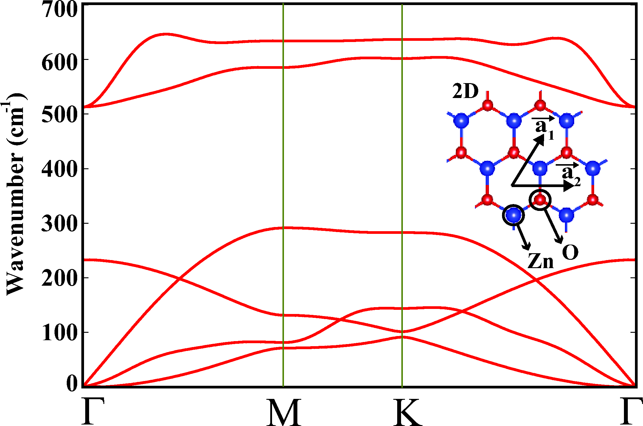
The structure of monolayer ZnO is optimized using periodically repeating supercell having hexagonal lattice in 2D and the spacing of 10 Å between ZnO planes. The optimized structure was planar and the magnitudes of the Bravais vectors of the hexagonal lattice are found to be Å, and the Zn-O bond, 1.895 Å (see Fig. 2). In contrast to 2D puckered honeycomb structures of Si, Ge and compounds of III and V group elements both lying below the first row, any honeycomb structure including one element from the first row form planar honeycomb structure like graphene, BN and SiC.hasan 2D monolayer of ZnO forming planar honeycomb structure is not an exception. The calculated structural parameters are significantly larger than those of graphene and BN honeycomb structure due to fact that Zn has larger radiusradius than that of B,C,N and O atoms. The planar structure of 2D ZnO is tested by displacing Zn and O atoms arbitrarily from their equilibrium positions by 0.5 Å and subsequently by re-optimizing the structure. Upon optimization the displaced atoms have recovered their original positions in the same plane. It should be noted that, the length of Zn-O bonds of 2D ZnO honeycomb structure is smaller than that in the 3D bulk (wz, zb) crystals, since bonding in the former is stronger than the tetrahedrally coordinated bonding in the latter. Similar trend is also found in C, BN and SiC honeycomb structures. The interaction between ZnO planes appears to slightly weaken the Zn-O bonds of h-ZnO crystal. As a result the length of the Zn-O bonds becomes larger than that of 2D ZnO honeycomb structure. The cohesive energy of 2D monolayer of ZnO is calculated to be 8.419 eV per Zn-O pair. This energy is 0.5 eV smaller than that of 3D wz-ZnO.
IV.1 Atomic structure and stability analysis
It should be noted that 2D honeycomb structure determined by the structure optimization using conjugate gradient method may not be necessarily stable. One needs more stringent tests to assure the stability of this truly 2D structure. As a matter of fact, it was argued earlier that any crystal structures consisting of a truly 2D monolayer crystals cannot be stable.stability1 ; stability2 Here, we summarize our analysis on the stability of planar 2D hexagonal structure of ZnO using calculation of phonon dispersion curves as well as ab-initio finite temperature molecular dynamics calculations.
We calculated optical and acoustical branches of phonon frequency using the density functional perturbation theory (DFPT) with plane wave method as implemented in PWSCF software and the force constant methodalfe with forces calculated using VASP. The former method includes the polarization effects so that the splitting of longitudinal and transverse optical modes at the -point (namely LO-TO splitting) is obtained. The force constant method cannot yield the LO-TO splitting and is also very sensitive to the mesh size in calculating forces under atomic displacements and hence in setting up the dynamical matrix. In fact, the imaginary frequencies of ZA branch (so called out of plane acoustical branch) occur around the -point as an artifact of insufficient mesh size. However, all imaginary frequencies around the -point (corresponding to an instability to be induced by acoustical waves with large ) are removed by using very fine mesh. Earlier, imaginary frequencies of ZA modes near the -point calculated for 2D honeycomb structures of Ge and III-V compounds inducing similar fortuitous instabilities for large were also removed by using finer mesh.hasan
In Fig. 2 we present phonon dispersion calculated for 2D monolayer of ZnO honeycomb structure using force constant method, where atomic forces are calculated by VASP. Calculated phonon modes all being positive across the BZ strongly support that 2D monolayer of ZnO is a stable structure corresponding to a local minimum on the Born-Oppenheimer surface. Our phonon dispersion curves are in agreement with those calculated in Ref[phonon, ].
Furthermore, we have tested the stability of 2D ZnO monolayer using finite temperature ab initio molecular dynamics (MD) calculations with time steps of 2x10-15 seconds. To lift the constraints to be imposed by a small unit cell, we considered a (77) supercell of the 2D hexagonal ZnO and raised its temperature from 0 K to 750 K in 0.1 ps. Then, we have kept the temperature of the system around 750 K for 2.5 ps. While all these calculations resulted in minor deformations, the honeycomb structure was not destroyed. It should be noted that these calculations may not be conclusive, since 2.5 ps cannot be sufficient to represent all the statistics, but this picture is the best one can see from the exiguous window limited by the computational cost imposed by ab-initio MD method. In the following sections we will present additional arguments related with electronic structure, which further corroborate the stability of 2D ZnO structures.
IV.2 Electronic Structure
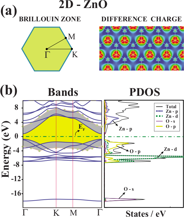
The difference charge density and the electronic energy bands together with the partial density of states are presented in Fig. 3. Contour plots of total charge indicate high density around O atoms. The difference charge density is calculated by subtracting charge densities of free Zn and O atoms from the total charge density of 2D ZnO, i.e. . High density contour plots around O atoms protruding towards the Zn-O bonds indicate charge transfer from Zn to O atoms. This way the Zn-O bond acquires an ionic character. The charge transfer from Zn to O, q is analyzed by using different schemes. The charge transfer values calculated by Löwdin method using PWSCF , Baderbader analysis using VASP, and local basis set analysis using SIESTA are, respectively, =1.35, 1.18 and 0.87 electrons. Interestingly, as compared to 3D bulk h-ZnO crystal, the charge transfer from cation to anion of 2D monolayer ZnO is slightly decreased. This is due to the change from hybrid orbital in h-ZnO to hybrid orbital in honeycomb structure.
Two dimensional ZnO is a direct band gap semiconductor with a gap value of 1.68 eV. However, the actual band gap is expected to be larger. The bands are corrected using methodgw and the direct band gap at the -point of BZ is found to be 5.64 eV. Much recently, it has been reported that the band gap of 2D-ZnO is calculated to be 3.57 eV with GW corrections.phonon Similar to the bands of 3D bulk ZnO crystals, the upper part of the upper valance band are derived mainly from O- orbitals, whereas the lower part has Zn- character. The bands at the edges of conduction and valence bands along the - direction are derived from bonding and antibonding combination of O- and Zn- orbitals forming - and -states. The highest valence band along the - direction has mainly O- but small Zn- orbital contribution, while the lowest conduction band is composed mainly from Zn- but small O- orbitals. Small Zn- contribution is also confirmed by PDOS. Consequently, planar geometry of 2D monolayer of ZnO is expected to be attained by the bonding combination of -states. The same situation occurs for 2D monolayer of BN honeycomb structure, which is an ionic III-V compound with wide band gap between - and -states. The planar stability graphene is also maintained by -bonds.
IV.3 Vacancy Defects and Antisite
It was shown that vacancies have remarkable effects on electronic and magnetic properties of 2D graphene and graphene nanoribbons.esquinazi ; Iijima ; yazyev ; guinea ; brey2 ; topsakal_delik To the best of our knowledge, the effects of vacancies in monolayer of ZnO have not been treated yet. It was reported that the vacancy defects can be intentionally created by electron irradiation methodannihilation on ZnO thin films. We investigated the effects of Zn-, O-, Zn+O-divacancy and O+Zn-antisite in a periodically repeating (55) as well as (77) supercells. The vacancy-vacancy coupling in the larger (77) supercell was reduced significantly. Flat bands in the band gap have charge density localized at the defect site. The width of these flat bands can be taken as the measure of the strength of the direct and indirect (via the hopping through the orbitals in the lattice) vacancy-vacancy coupling. The largest width of such a band is already small (less than 50 meV). The average energy of these flat bands from the top of the valence band can be taken as the localized states of an individual vacancy defect. Our results obtained using a (77) supercell are presented in Fig. 4 and discussed in the rest of the section.

The GGA band gap of a defect-free, 2D monolayer ZnO increases by 0.08 eV in a (77) supercell including a vacancy defect. This is an artifact of the model, which mimics an individual vacancy in supercell having limited size. First we generated a Zn-vacancy by removing a single Zn atom from the monolayer of ZnO in honeycomb structure as shown in Fig. 4 (a). Upon the structure optimization, two O atoms around vacancy are departed from the plane. Similar to the vacancies in graphene and BN, Zn-vacancy induces a local magnetization in the system. Isovalue surfaces of spin density difference clearly reveals the magnetism around vacancy. The calculated total magnetic moment is 2 per unit cell. Note that similar Zn-vacancy in the 3D bulk ZnO crystal induces a magnetic moment of 1 . It should be noted that the magnetic moment of Zn-vacancy arises from the unpaired electrons of oxygen atoms around the Zn vacancy. Therefore it is important to determine precisely whether the vacancy induced localized states are occupied. The positions of these localized states of 2D ZnO calculated for the (77) supercell and their occupancy unambiguously comply with the calculated magnetic moment. The Zn-vacancy in a repeating (77) supercell also modifies the electronic structure. The value of the band gap of defect-free ZnO changes from 1.68 eV to 1.75 eV, and a spin up localized state appear 0.25 eV above the top of the valence band. Figure 4 (b) presents our results for O-vacancy. Unlike the case of Zn-vacancy, the monolayer of ZnO containing an O-vacancy is nonmagnetic. Zn atoms around vacancy with coordination number 2 prefer to stay in the same plane of the other atoms and do not induce any magnetization. The band gap is slightly modified to 1.80 eV. As for Zn+O divacancy in Fig. 4 (c), it is again nonmagnetic. The band gap is also modified to 1.46 eV. Four occupied states associated with divacancy occur as localized states in the band gap. Finally, we consider the antisite defect. The resulting relaxed structure is given in Fig. 4 (d). The antisite O is pushed away from Zn atoms and makes bonds with a nearby O atom. The system does not show any magnetization. The energy of final structure with antisite defect is 5 eV higher (i.e. energetically less favorable) that of the defect-free 2D monolayer of ZnO. The antisite induces two localized states in the band indicated in the figure. Also it is noted that the magnetic moments calculated for single Zn- and O-vacancy do not agree with Lieb’s theorem,lieb which predicts the amount of magnetic moments for carbon vacancies in 2D graphene. According to Lieb’s theorem, the net magnetic moment per cell is expected to be =1 for Zn and O vacancies in Fig. 4. This might be related with the ionic bonding which is different from graphene or the existence of d-orbitals in Zn. On the other hand, zero magnetization for Zn+O divacancy in Fig. 4 (c) is in agreement with the theorem.
IV.4 2D ZnO bilayer
Recently, Tusche et al.bilayer revealed two monolayer of ZnO grown on Ag(111) substrate using surface x-ray diffraction and scanning tunneling microscopy. They also showed that the transition to the bulk wz-ZnO structure occurs in the 3-4 monolayer coverage. The Zn-O bond length of the planar hexagonal structure measured 1.93 Å is slightly larger than the the value of 1.895 Å calculated for the the bond length of the monolayer of ZnO. This situation implies that the effect of the Ag(111) substrate may be negligible.bilayer
We investigated the atomic structure and stability of bilayer ZnO honeycomb structure. To determine the minimum energy configuration we used periodic supercell geometry and considered five different stacking types which are , , , and . In configuration, Zn (O) atoms of the second layer are on top of the Zn (O) atoms of the first layer. is similar to except that Zn atoms are above O atoms. , and configurations are obtained by shifting one of the layers of and on the other layer, so that Zn or O atoms of the second layer are placed above the center of the hexagons in the first layer. It is () if O (Zn) atoms of both layers face the centers of hexagons. corresponds to the configuration where O (Zn) atom of the first (second) layer face the center of second (first) layer.
Among these five configurations we found that is energetically most favorable. , , and configurations have respectively 0.213, 0.312, 0.320 and 0.321 eV (per primitive cell) higher energies than configuration. The length of Zn-O bonds as well as the charge transfer from Zn to O in configuration is slightly larger than the value of 1.895 Å calculated for the the bond length of the monolayer of ZnO. This trend complies with the above discussion that the bond length increases by going from 2D monolayer to 3D bulk and implies that the effect of the Ag(111) substrate may be negligible.bilayer
The bilayer binding energy among two ZnO layers is calculated to be 0.162 eV (per Zn-O pair) by subtracting the total energies of two individual monolayers from the total energy of bilayer ZnO in configuration. Furthermore the layer-layer separations are calculated as 4.02, 2.36, 3.80, 3.78 and 2.68 Å for , , , and respectively. Hence, bilayer formation is exothermic. The calculations with LDA, which accommodate van der Waals interaction between layers better, yields 0.297 eV (per Zn-O pair) binding energy between two ZnO layers and 2.267 Å layer-layer separation in structure. The layer-layer separation for is experimentally reported as 2.314 Å.bilayer The difference between the lattice constants of the monolayer 2D ZnO honeycomb structure and the ZnO bilayer is small. Owing to the relatively weak coupling between two ZnO monolayers, the calculated electronic structure is similar to that of single layer ZnO honeycomb structure, except that the band gap decreases to 1.44 eV for . This band gap increases to 5.10 eV after the GW0 correction, which is still smaller than the GW0 corrected band gap of 2D monolayer ZnO.
We next address the question whether the structure of 2D bilayer formed by the stacking of the ZnO bilayer is stable is examined by the finite temperature ab-initio molecular dynamics and phonon frequency calculations. Ab-initio molecular dynamics calculations at 750 K are performed with the same parameters as done for the monolayer ZnO in previous section indicate that the bilayer remains stable at 750 K after 3.0 ps.
| ZnO | Bonding | (eV/atom) | GGA | Exp | ||||
|---|---|---|---|---|---|---|---|---|
| 3D | 2.001-2.007 | 8.934 | 0.75 | 2.76 | 3.29 | 2.44 hamada | 3.37 bulk_zno | |
| 3D | 2.001 | 8.919 | 0.65 | 2.53 | 3.09 | 3.59 zb_gw | ||
| 3D | 1.999 | 8.802 | 0.96 | 2.84 | 3.32 | |||
| 2D bilayer | 1.932 | 8.640 | 1.44 | 4.45 | 5.10 | |||
| 2D monolayer | 1.895 | 8.478 | 1.68 | 4.87 | 5.64 | 3.57 phonon |

V Dimensionality Effects
A comparison of Zn-O bond length, cohesive energy, GGA bad gap, GW0 corrected band gap calculated for 3D wz-, zb-, h-ZnO, 2D bilayer and monolayer of ZnO are presented in Table-I, where interesting dimensionality effects are deduced. These dimensionality effects are believed to be crucial for better understanding of 2D crystals. Quasi 1D nanoribbons are not included to this discussion because of edge effects of the ribbon.
Three dimensional crystals have larger number of nearest neighbors and also posses larger Madelung energy as compared to 2D crystals. wz-ZnO appears to correspond to the global minimum of ZnO II-VI compound. However the energy difference between wz-ZnO and 2D monolayer of ZnO is only 0.5 eV and is smaller than one expects. It appears that -like bonding which is stronger than -like bonding and the -bonding between adjacent orbitals, which contributes to stability by maintaining the planar geometry give rise to the relatively smaller energy difference between 3D and 2D monolayer ZnO. In the absence of significant -bonding one expects that 2D planar ZnO would be buckled (puckered) for stability as found in 2D Si and GaAs honeycomb structure.seymur ; hasan Through puckered planar orbital is dehybridized and is transformed to -like hybrid orbitals. Here we note that population of oxygen and orbitals is larger than that of corresponding Zn orbitals, since the former significantly higher electronegativity.
Interestingly, while GGA bad gaps of 3D ZnO occurs 0.75-0.96 eV, the band gaps of in 2D is 1.68-1.44 eV. The band gap in 2D is larger than 3D, since the energy difference between -like orbitals of Zn and O ions is smaller than the energy difference of -orbitals. The latter gives rise to larger energy difference between bonding and antibonding orbitals. These band gaps are, however, underestimated by GGA, since they increase approximately three times upon GW0 corrections. It appears that band gap values corrected by GW0 is closer to experimental value and hence superior to GW correction. As for as , and are concerned, 3D h-ZnO is intermediate between 3D and 2D structures. Also calculated values of bilayer ZnO are slightly closer to 3D than those of 2D monolayer of ZnO.
Charge transfer from Zn to O is crucial for dimensionality effects, but difficult to calculate precisely. Charge transfer, , calculated using three different schemes, namely Löwdin, Bader and Siesta, yield different but consistent values. For example, the Löwdin values occur around 1.4 electrons for 3D, but relatively smaller value of 1.35 electrons for 2D. Bader analysis yields 1.22-1.20 electrons for 3D, and relatively smaller value of 1.18 electrons for 2D. As for Siesta, 3D values, they are 0.90 electrons for 3D, but 0.87 electrons for 2D. Excluding the paradoxical situation with charge transfer values of zb-ZnO occurring close to those of 2D ZnO, the charge transfer between Zn and O is slightly smaller in 2D than 3D.
VI ZnO Nanoribbons
In this section, we consider bare and hydrogen passivated armchair (a-ZnO) and zigzag (z-ZnO) ZnO nanoribbons. These nanoribbons are specified according to their width given in terms of number of Zn-O pairs in their unit cells. Hence, z-ZnO() indicates a zigzag ZnO nanoribbons having Zn-O pairs in their unit cell. We investigate their electronic, magnetic and mechanical properties. First, we start with the stability analysis of these nanoribbons.
VI.1 Stability Analysis
We have analyzed the stability of the bare armchair ZnO nanoribbons having Zn-O atom pairs in the unit cell using the force constant method and the finite temperature molecular dynamics calculations. The dynamical matrix was generated using the forces calculated in seven unit cells of a-ZnO(9). Results of this calculation were presented in Fig. 5 (a). Phonon dispersion curves of quasi 1D nanoribbons, in general, show profiles expected from the folding of 2D phonon dispersion curves. Modes appearing above 700 , however, are not expected from this folding. They were attributed to edge effects and reconstructions.
Right panel of Fig. 5 (a) presents the acoustic region in ten times magnified scale. There are four acoustic modes, dispersion curves of which go to zero as k 0. To get exactly zero value, we have imposed the symmetries originating from translational and rotational invariance on the dynamical matrix. To impose these symmetries we have tuned the force constant matrix elements so that all forces on all atoms are zero when the whole structure is shifted in three dimensions or slightly rotated along the axis passing through the middle of the nanoribbon.
Both the longitudinal and transverse acoustic modes have linear dispersions near the point. Group velocity of LA mode is slightly higher than that of TA mode. Out of plane ZA and twisting acoustical TW modestwisting have quadratic dispersion near the point, which is attributed to the rapid decay of the force constants with increasing neighbor distance. In fact there are some imaginary frequencies in ZA mode near the point. The absolute value of these frequencies do not exceed 0.5 and they are purely an artifact of the precision of the numerical calculation. Using a finer mesh makes these imaginary frequencies disappear.
We also have calculated vibrational modes of the finite patch of ZnO having the length of five unit cells and the width of . Zigzag edges of this flake were saturated by hydrogen atoms to eliminate the magnetism and to simplify the numerical computations. Vibrational spectrum of this structure had no imaginary frequencies implying the fact that finite size flakes of 2D ZnO honeycomb structure is stable. The density of states, DOS of calculated phonon frequencies are presented in Fig. 5 (b). Note that, DOS calculated for three different honeycomb systems are similar. Owing to the edge effects the gap between the acoustical and optical branches of the ribbon is reduced. Similar effect as well as broadening of discrete mode frequencies cause DOS of the flake to deviate significantly from that of 2D honeycomb structure in the gap. The vibrational modes attributed to strong Zn-H and O-H bonds are centered respectively at 1830 and 3700 . These modes are not shown, since these frequencies are beyond the range of Fig. 5 (b).
Ab initio molecular dynamic calculations were also carried out for a-ZnO(9) and a finite size patch of it. To eliminate constraints to be imposed by small unit cell, the infinite nanoribbon is treated by a supercell composed of five unit cells. Both nanoribbons are kept at 750 K for 3.5 ps. As a result, infinite, periodic structure of a-ZnO(9) composed of five unit cells had minor reconstructions at the edges, while its honeycomb structure was preserved. Finite structure had the similar pattern at the armchair edges, but the reconstructions at the hydrogen saturated zigzag edges were more pronounced. These reconstructions made the whole system bend, but again the honeycomb structure was preserved around the central region of the nanoribbon. The results of this analysis are interpreted that finite size ZnO nanoribbons are stable.
VI.2 Electronic and Magnetic Properties
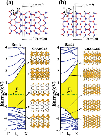
Bare and hydrogen terminated a-ZnO nanoribbons are nonmagnetic semiconductors with direct band gaps which are relatively larger than that of the monolayer ZnO. Fig. 6 (a) and (b) shows the atomic and electronic structure of bare and hydrogen terminated a-ZnO() with =9. The atoms at the edges of the bare a-ZnO are reconstructed; while one edge atom, Zn is lowering, adjacent edge atom, O is raised. The energy band gap calculated with GGA is direct and 1.92 eV wide and is larger than the band gap of 2D monolayer ZnO. Band decomposed charge density analysis of a-ZnO(9) is presented in Fig. 6. The highest valance bands are degenerate and their charge accumulates on oxygen edge atoms for bare ribbon. The third band from the top of valence band is also associated with edge states. On the other hand, the charge of the lowest conduction band is distributed uniformly in the ribbon. The charge of the second conduction band is mostly distributed at the dangling bonds on the edges of the ribbon.
The passivation of Zn and O atoms at the edges by hydrogen atoms gives rise to changes in the electronic band structure. The bond lengths Zn-H and O-H bonds are calculated to be 1.53 and 0.97 Å. As seen in Fig. 6 (b), upon passivation with hydrogen atoms, the reconstruction of edge atoms are weakened. At the end the edge state bands are discarded from the band gap and replaced by dispersive bands having charge distributed uniformly in the ribbon. The band gap of H-passivated a-ZnO(9) slightly increases to 1.98 eV.
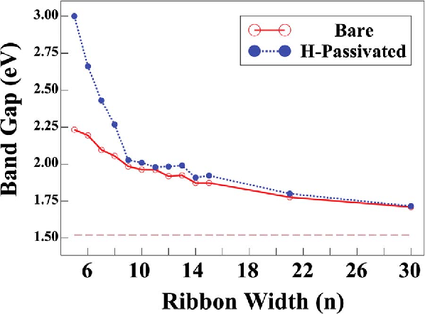
The variation of the band gap for the bare and hydrogen saturated armchair nanoribbons as a function of is given in Fig. 7. The band gaps are large for small but approaches to those of 2D honeycomb structure as the width . This is an indication of the quantum size effect. For <9, the value of the band gap of hydrogen passivated a-ZnO is significantly larger than that of bare ribbons; the difference practically disappears for >20. In contrast to graphene and BN nanoribbons, family dependent variations of band gapfamily-dep-gaps is absent in Fig. 7. The variation of the band gap with is an important property, which may lead to formation of quantum dot or multiple quantum wells through the size modulation.gribbon4
Earlier it has been reportedmendez1 ; mendez2 that all a-ZnO nanoribbons are semiconductors with a constant band gap of 2 eV. In our case, however, the band gaps of nanoribbons, especially for n<10, display apparent dependency on n. The tendency of the decrease in the band gaps to the 2D ZnO band gap is also observed when n is increased.
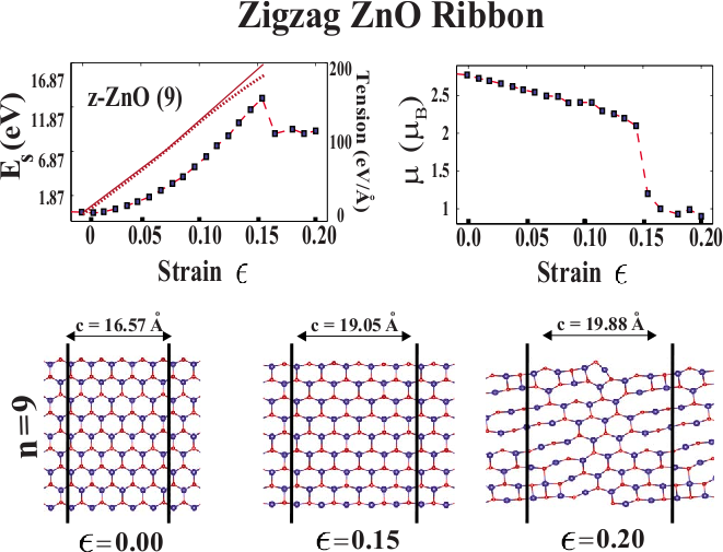
In contrast to a-ZnO nanoribbons, all zigzag nanoribbons (z-ZnO) we investigated in this work (namely n=5,7,9) show metallic character regardless of their widths. On the other hand, while all a-ZnO nanoribbons are nonmagnetic, bare z-ZnO nanoribbons are magnetic due to edge states. The magnetic properties of z-ZnO depend on whether the edge atoms are passivated with hydrogen. Our results regarding with the bare and hydrogen passivated z-ZnO() nanoribbons for =9 are presented in Fig. 8 (a)-(c). In Fig. 8 (a), while the upper edge of the ribbon is made by O atoms, the lower edge terminates with Zn atoms. The bare z-ZnO nanoribbon is magnetic, since the spin polarized calculations yield the total energy, which is energetically 34 meV favorable than that obtained from spin unpolarized calculations. The total magnetic moment of the system was calculated as 0.57 per unit cell. Figure 8 (b) shows total density of states (DOS) and band structure of bare z-ZnO(9) together with isosurface charge densities of selected bands. Bare z-ZnO(9) have isosurfaces of difference charge density occur around O edge atoms due to unpaired O- orbitals. Clearly, bare z-ZnO is a ferromagnetic metal. These results are in agreement with those predicting that the ferromagnetic behavior of ZnO nanoribbons due to unpaired spins at the edges is dominated by oxygen atoms.mendez1 ; mendez2

The band structure of the nanoribbon gives us further information about the magnetism of the system. When we plot the spin-up and spin-down bands we observe the splitting of these bands around Fermi level. The conduction and lower valance bands are degenerate for spin-up and spin-down states, some of which are shown with yellow isosurface charge densities in the figure. We also plotted charge density of two states of spin-split nondegenerate bands. Spin-down state is half-filled, while spin-up state is totally filled. Furthermore, their charges are confined to the O-edge of the ribbon. The spin polarization at the Fermi level is calculated in terms of density of spin up and spin down states, , namely and is around 80 % for spin-down states although the spin-up states are majority spins. This suggests z-ZnO() with high spin polarization at can operate as spin valve device.
As we discussed in Sec. IV.3, the magnetism of Zn-vacancy in the monolayer ZnO is directly related with O atoms having unpaired orbitals. Similarly, bare z-ZnO nanoribbons have also magnetic states on O terminated edge of the ribbon. The splitting of spin-up and spin-down bands around Fermi level is removed when the edges of bare z-ZnO(9) in Fig. 8 (a) is passivated by hydrogen. The resulting structure is again metallic but nonmagnetic. The electronic properties of the z-ZnO(9) ribbon passivated with hydrogen is presented in Fig. 8 (c). Two bands just below the Fermi level is localized on the Zn edge of the ribbon and lowest conduction band is localized on the O edge of the ribbon. Similar results are also obtained for n=5 and n=7. The situation regarding the magnetism of bare z-ZnO is somewhat different from that of the bare zigzag graphene nanoribbons, which have ferromagnetic coupling along the edges, but antiferromagnetic coupling between the edges.gribbon1 Moreover, unlike the case in z-ZnO nanoribbons, the magnetism of zigzag graphene nanoribbons are not destroyed upon termination of edges with hydrogen atom.
An important feature of of zigzag ZnO nanoribbons is that charged Zn and O atoms terminate different edges and thus induce sizable electric dipole moments. For the bare z-ZnO(9) the dipole moment is calculated to be 0.78 (electronÅ) per cell. Upon H termination of Zn and O edge atoms the dipole moment increases to 1.07 (electronÅ) per cell and its direction is reversed. While the dipole effects are included in the electronic structure calculations of H-terminated z-ZnO(9) nanoribbons, the band gap under estimated by GGA may effect its metallicity. Unfortunately, GW0 corrections cannot be applied due to large number of atoms.
VI.3 Mechanical Properties of ZnO Nanoribbons
The response of the nanoribbons to the applied uniaxial stress is crucial and provides information on the strength of the nanoribbons. More recently, the response of graphene to strain (or to tension) in the elastic deformation range has been an active field of study. For example, recent worksstraineffect indicated the effect of deformation on the electronic properties for band gap engineering. Moreover theoretical studiesmehmet3 have shown that carbon atomic chain can be derived from graphene under tension. C. Jin et al.carbonchain showed that carbon atomic chains can be derived from graphene by electron irradiation inside a transmission electron microscope. Therefore, the response of ZnO nanoribbons to tension is of crucial importance.
Owing to ambiguities in defining the cross section of the ribbon one cannot determine the Young’s modulus rigorously. We examined the variation of the strain energy, with respect to the applied uniaxial strain, , being the lattice constant along the ribbon axis. The variation of includes information regarding the mechanical properties of the ribbon. For example, force constant, is obtained from the variation of . is an observable and can specify the strengths of ribbons unambiguously. The effects of two edges due to incomplete hexagons becomes important for narrow nanoribbons, but decrease with increasing width. In-plane stiffness C, which is independent of the thickness, can also be used instead of Young’s modulus. Defining as the equilibrium area of the system, C can be given as
| (2) |
By choosing a reasonable thickness “h”, Young’s modulus can be recalled as Y=C/h. The thickness value around 3.34 Å was used in order to evaluate the elastic properties of SWNTs and graphene by some works in literature.yakobson1 ; yakobson2 ; dereli We note that while is unique for 2D infinite (periodic) honeycomb structure of ZnO, for nanoribbons it depends on how the width of the ribbon is taken in determining . In fact, the width of the a-ZnO nanoribbon cannot be determined straightforwardly. It is not clear whether the distance is from Zn at one edge to Zn at the other edge, or from O at one edge to other O. One can also take the average of these two, or consider charge spill over from these edge atoms. Hence the value of is subject to small changes depending on how the width of the nanoribbon is taken. This uncertainty, however, diminish as the width increases; eventually the value of converges to a fixed value. In this respect, once the width is fixed , can be determined from .
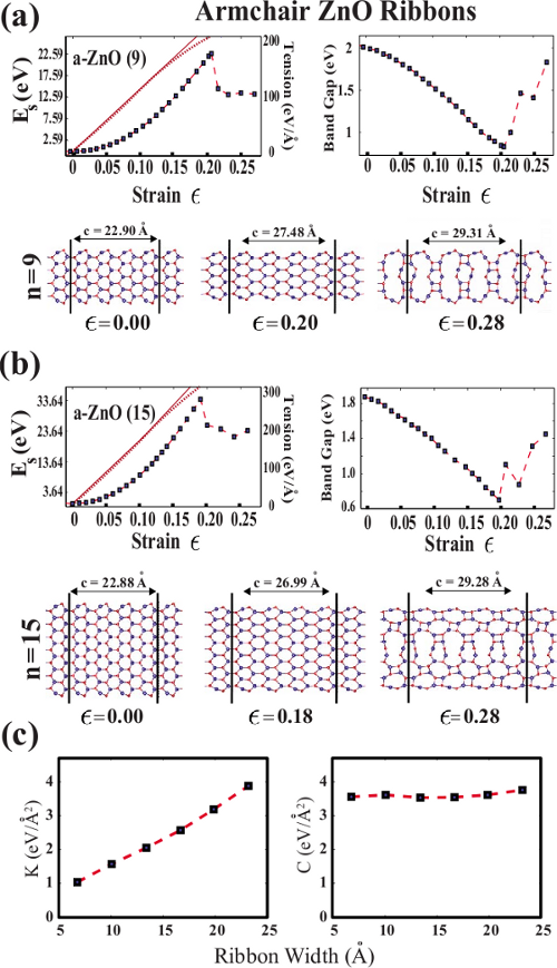
We considered three nanoribbons, a-ZnO(9), a-ZnO(15) and z-ZnO(9). In order to eliminate the constraints imposed by the periodic boundary conditions of small unit cell, calculations are performed using a supercell composed of four primitive unit cells for a-ZnO and five unit cells for z-ZnO. The size of supercells is determined based on certain tests. Figure 9 (a) and (b) show the variation of the strain energy and band gap with the applied strain, for both ribbons, a-ZnO(9) and a-ZnO(15). They display a parabolic vs curves up to the strains 0.13. Beyond these strain values, energy vs strain variation becomes elastic but anharmonic. In the elastic range, the ribbons preserve their honeycomb like structure, but the hexagons are elongated uniformly along the direction of the strain. Zones of harmonic and anharmonic variation of can be better deduced by calculating the tension force, . is linear for in the elastic-harmonic range, but becomes nonlinear for as seen in Fig. 9(a) and (b). If the applied tension is released, the elastic deformation in both harmonic and anharmonic ranges disappears and the ribbon returns to its original equilibrium geometry.
The elastic deformation range of a-ZnO(9) and a-ZnO(15) ends with a sharp fall of the total energy. This point is identified as the yielding point of the ribbon occurring at 0.20. The yielding points are followed with structural transformation, where honeycomb cage structure starts to undergo a change and part of the strain energy is relieved. Once the yielding point is passed the ribbon can stretch under significantly low tension and some fraction of the deformation will be permanent and irreversible if the tension is released. Similar behavior occurs when a nanowire of metals, such as Au or Cu; following an order-disorder transformation the elastic deformation ends and the wire is elongated by one lattice constant (or it deforms plastically). However, in contrast to the present case, the nanowire attains again the ordered state and start to deform elastically.mehrez
The force constant is calculated to be =2.05 and 3.88 eV/Å2 for a-ZnO(9) and a-ZnO(15), respectively. The increase of from 2.05 eV/Å2 to 3.88 eV/Å2 is due to the increase of the width from =9 ( 12.81 Å) to =15 ( 22.65 Å). Note that if the Hooke’s law were valid for these nanoribbons, the ratio would be equal to the ratio of widths, namely 22.65/12.81=1.77. The calculated value (3.88/2.05=1.89) is slightly higher. The discrepancy arises from the edges of the ribbons, which respond to tension differently from the central region. Therefore, deviation from the Hooke’s law becomes more serious as decreases, but diminish as . values of a-ZnO(9) and a-ZnO(15) calculated for primitive unit cell are 7.92 eV/Å2 (instead of 4 2.05=8.20 due to numerical calculations performed in a large supercell) and 15.04 eV/Å2 (instead of 4 3.88=15.52), respectively. These values are smaller than those corresponding to graphene ( 40.96 and 72.52 eV/Å2 ) and BN ( 34.02 and 60.46 eV/Å2 ) nanoribbons.
The calculated in-plane stiffness values for a-ZnO(9) and a-ZnO(15) are 3.75, 3.71 eV/Å2, respectively.stiffness The calculated C values of armchair graphene (BN) nanoribbons for n=9 and n=15 are 18.45 (14.55) and 18.85 (14.66) eV/Å2, respectively. Graphene and BN nanoribbons have significantly higher in-plane stiffness as compared to a-ZnO nanoribbons. The difference mainly originate from the fact that a-ZnO honeycomb structure has larger unit cell than that of graphene and BN honeycomb structures. In view of the calculated and values, both graphene and BN nanoribbons are stiffer than ZnO nanoribbons.
Figure 9 illustrates also the atomic structure of a-ZnO(9) and a-ZnO(15) nanoribbons for three different values of applied strain. After the yielding point, the honeycomb structure is destroyed and the polygons being smaller and larger than hexagons form. In some cases, a net magnetic moment can develop in those polygons. The onset of plastic range and variation of atomic structures can depend on the periodic boundary conditions. These artifacts of periodic boundary conditions are eliminated to some extent by using larger supercells comprising several unit cells. Nonetheless, the plastic deformations shown in Fig. 9 (a) and (b) have still large repeat periodicity. Even if the size and forms of polygons appear to be hysteric, their further investigation is of fundamental interest. The order-disorder structural transformation, as well as dislocation generation appear to be absent in this study. The latter may require a treatment of deformation by taking into account very large and . Moreover, as predicted for graphene nanoribbons, one expects that the onset of yielding in the presence of vacancy defects and also at high temperature can occur at small strain.mehmet3 Nevertheless, the plastic deformation in the present work is carried out under ideal conditions, hence its stochastic nature is not taken into account. The energy gap of the nanoribbon undergoes a significant change under uniaxial tension. It decreases as increases and becomes very small at the yielding point. Beyond the yielding point the band gap increases again.
In Fig. 9 (c) we plot the calculated values of force constant, relative to the width of a-ZnO() taken as the distance between outermost atoms of both edges. As expected is proportional to and can be considered as linear except small deviations from linearity due to edge effects. In fact, increases slightly with . Whether a-ZnO() has even or odd also causes to a small deviation from single linear variation. As expected, the variation of the in-plane stiffness with is not significant. However, changes significantly between two subsequent values of .
The zigzag z-ZnO(9) nanoribbon displays a variation similar to those of a-ZnO. The calculated value of is 4.27 eV/Å2, which is larger than that calculated for a-ZnO(9) having relatively smaller width. Similarly, in-plane stiffness value of z-ZnO(9) is slightly smaller than that of a-ZnO(9) and a-ZnO(15). C is calculated as 3.24 eV/Å2. The zigzag ZnO(9) remains to be ferromagnetic metal in the elastic deformation range, but their magnetic moment decreases with increasing . However, beyond the yielding point it shows a sharp fall and diminish with increasing in the plastic range as seen in Fig. 10. In contrast to a-ZnO, long polygons are aligned along the axis of the z-ZnO(9) in Fig. 10.
VII Discussion and Conclusions
This work presents an extensive study on 2D monolayer and bilayer ZnO, and ZnO nanoribbons together with their stability analysis. The monolayer of ZnO is an ionic and nonmagnetic, wide band gap semiconductor with significant charge transfer from zinc atoms to nearest oxygen atoms. Since DFT normally underestimates the calculated band gaps, the calculated band gap of specific structures are corrected by GW0 self-energy calculations. ZnO has 2D hexagonal lattice forming a planar honeycomb structure. Our predictions, which contribute to a better understanding of this material are emphasized by way of conclusions:
i) We have shown that, 2D ZnO monolayer and bilayer, quasi 1D bare nanoribbons of ZnO and 0D patch of ZnO correspond to local minima on the Born-Openheimer surface and thus are predicted to be stable. ii) Ab-initio molecular dynamics calculations performed at high temperature corroborate our analysis obtained from the calculation of phonon frequencies. iii) We performed calculations of phonon modes and density of states of phonon frequencies of 2D monolayer, quasi 1D armchair nanoribbon and a finite flake using force constant method. In particular, we revealed the acoustical twisting mode of armchair nanoribbon. iv) Our study of Zn-, O-, Zn-O-vacancies and O-Zn antisite indicates that local magnetic moments can be generated only by Zn-vacancies. v) We provided an extensive analysis of the electronic structure of hydrogen terminated, as well as bare armchair and zigzag nanoribbons. Armchair ZnO nanoribbons are found to be nonmagnetic semiconductors. The band gaps vary with their widths. The narrow nanoribbons have relatively larger band gap due to the quantum confinement effect. Bare zigzag ZnO nanoribbons are ferromagnetic metals. The atoms near the oxygen terminated edge of the ribbons acquire magnetic moments. The spin-polarization at the Fermi level may attain high values for specific zigzag nanoribbons. However, once O- and Zn- terminated edges are passivated with hydrogen atoms, the zigzag nanoribbon becomes nonmagnetic metal. These electronic and magnetic properties might be useful for spintronic applications. vi) We found the minimum energy stacking of the ZnO bilayer, and provided energetics and energy band structure corresponding to this stacking. Accordingly, bilayer ZnO is also a nonmagnetic, wide band gap semiconductor with slightly smaller band gap as compared to that of monolayer. vii) We provided an analysis of mechanical properties. ZnO nanoribbons under uniaxial strain show harmonic and anharmonic elastic deformation ranges and a yielding point. After yielding, the strain energy exhibits a sharp fall and the nanoribbon deform plastically. In the elastic range, hexagons are uniformly deformed, but honeycomb like atomic structure is maintained. After yielding point some of the hexagons are modified and reconstruct to different polygons which may be smaller or larger than hexagons. Variation of electronic and magnetic properties with deformation and formation of polygons in the plastic deformation range are of fundamental interest. Calculation of force constants and in-plane stiffness indicate that the stiffness of ZnO nanoribbons is smaller than those of graphene and BN honeycomb structures.
In summary, it is shown that single and bilayer ZnO and its nanoribbons in different orientations provide us for a variety of electronic and magnetic properties which may be interesting for further applications. Even if they have honeycomb structure common to monolayer graphene and BN, their properties exhibit important differences.
Acknowledgements.
We acknowledge stimulating discussions with Dr. Ethem Akturk. Part of the computations have been provided by UYBHM at Istanbul Technical University through a Grant No. 2-024-2007. This work is partially supported by TUBA, Academy of Science of Turkey.References
- (1) K. S. Novoselov, A. K. Geim, S. V. Morozov, D. Jiang, Y. Zhang, S. V. Dubonos, I. V. Grigorieva, A. A. Firsov, Science 306, 666 (2004).
- (2) Y. Zhang, Y.-W. Tan, H. L. Stormer, P. Kim, Nature 438, 201 (2005).
- (3) C. Berger, Z. Song, X. Li, X. Wu, N. Brown, C. Naud, D. Mayou, T. Li, J. Hass, A. N. Marchenkov, E. H. Conrad, P. N. First, W. A. de Heer, Science 312, 1191 (2006).
- (4) K. S. Novoselov, D. Jiang, F. Schedin, T. Booth , V. V. Khotkevich, S. Morozov, A. K. Geim, Proc. Natl. Acad. Sci. U.S.A. 102, 10451 (2005)
- (5) Y. W. Son, M. L. Cohen, S. G. Louie, Phys. Rev. Lett. 97, 216803 (2006).
- (6) Y.-W. Son, M. L. Cohen, S. G. Louie, Nature 444, 347 (2006).
- (7) M. Y. Han, B. Özyilmaz, Y. Zhang, P. Kim, Phys. Rev. Lett. 98, 206805 (2007).
- (8) H. Sevinçli, M. Topsakal, E. Durgun, S. Ciraci, Phys. Rev. B 77, 195434 (2008).
- (9) C-H Park and S. G. Louie, Nano Letters 8, 2200 (2008).
- (10) V. Barone, J. E. Peralta, Nano Letters 8, 2210 (2008)
- (11) M. Topsakal, E. Akturk, and S. Ciraci, Phys. Rev. B 79, 115442 (2009).
- (12) S. Cahangirov, M. Topsakal, E. Akturk, H. Sahin and S. Ciraci, Phys. Rev. Lett. 102, 236804 (2009).
- (13) H. Sahin, S. Cahangirov, M. Topsakal, E. Bekaroglu, E. Akturk, R. T. Senger, and S. Ciraci, Phys. Rev. B 80, 155453 (2009).
- (14) Claeyssens, J. Mater.Chem. 15, 139 (2005).
- (15) A. J. Kulkarni, M. Zhou, K. Sarasamak, and S. Limpijumnong, Phys. Rev. B 97, 105502 (2006).
- (16) Y. Wang, X. Fan, J. Sun, Materials Letters 63, 350 (2009).
- (17) Y. Huang , J. He, Y. Zhang , Y. Dai , Y. Gu , S. Wang , C. Zou, J. Mater. Sci. 41, 3057 (2006).
- (18) J. Duan, X. Huang , E. Wang, Materials Letters 60, 1918 (2005).
- (19) G.S Wu , T. Xie , X.Y Yuan, Y.Li , L. Yang , Y.H Xiao, L.D Zhang, Solid State Communications 134, 485 (2005).
- (20) C. Tusche, H.L. Meyerheim and J. Kirschner, Phys. Rev. Lett. 99, 026102 (2007).
- (21) D-K. Hwang, M-S. Oh, J. Lim and S-J. Park J. Phys. D: Appl. Phys. 40, R387 (2007).
- (22) M. Law, L. E. Greene, J. C. Johnson, R. Saykally and P. Yang, Nature 4, 455 (2005).
- (23) Z.Q Chen M. Maekawa, A. Kawasuso, S. Sakai and H. Naramoto , Physica B 306, 376 (2006) 722-725.
- (24) Q. Wang, Q. Sun, G. Chen, Y. Kawazoe, and P. Jena, Phys. Rev. B 77, 205411 (2008).
- (25) P. E. Blochl, Phys. Rev. B 50, 17953 (1994).
- (26) J. P. Perdew, J. A. Chevary, S. H. Vosko, K. A. Jackson, M. R. Pederson, D. J. Singh, C. Fiolhais, Phys. Rev. B 46, 6671 (1992).
- (27) The capacity of spin-polarized DFT and its comparison with other well-known methods can be found in a review article: "Spin-Polarized DFT Calculations and Magnetism" by R. Zeller in Computational Nanoscience:Do It Yourself, J. Grotendorst, S. Blugel and D. Marx (Eds.) John von Neumann Institute for Computing, Julich, NIC Series, Vol. 31, ISBN 3-00-017350-1 pp. 419-445, (2006).
- (28) G. Kresse, J. Hafner, Phys. Rev. B 47, 558 (1993).
- (29) G. Kresse, J. Furthmuller, Phys. Rev. B 54, 11169 (1996).
- (30) S. Baroni, A. Del Corso, S. Girancoli and P. Giannozzi, http:/www.pwscf.org/.
- (31) J. M. Soler, E. Artacho, J. D. Gale, A. Garcia, J. Junquera, P. Ordejon, and D. Sanchez-Portal, J. Phys.: Condens. Matt. 14, 2745-2779 (2002). Calculations are performed within GGA. A double- plus polarization basis set was used. A charge density cutoff of 400 Ry was used.
- (32) M. Shishkin, G. Kresse, Phys. Rev B 74, 035101 (2006).
- (33) Ü. Özgür, Ya. I. Alivov, C. Liu, A. Teke, M. A. Reshchikov, S. Doǵan, V. Avrutin, S.-J. Cho, and H. Morkoç, J. Appl. Phys. 98, 041301 (2005).
- (34) M. Catti, Y. Noel, and R. Doves, J. Phys. Chem. Solids, G4, 2183 (2003); see also J.E. Jaffe and A.C. Hess, Phys. Rev. B 48, 7903 (1993).
- (35) J. Haffner, J. Comput. Chem. 29 , 2044 (2008).
- (36) M. Oshikiri, F. Aryasetiawan, Phys. Rev. B 60, 10754 (1999).
- (37) M. Usuda, N. Hamada, T. Kotani, M. vanSchilfgaarde, Phys. Rev. B 66, 125101 (2002).
- (38) P.-O. Löwdin, J. Chem. Phys. 18, 365 (1950).
- (39) G. Henkelman, A. Arnaldsson, H. Jonsson, Comput. Mater. Sci. 36, 254-360 (2006).
- (40) Calculated effective charge of Zn atom indicating 1 electron occupancy of the valance orbitals eliminates the inert gas configuration. Therefore, one considers the covalent radii, namely RZn=1.31 Å and RO=0.66 Å.
- (41) R. E. Peierls, Ann. I. H. Poincare 5, 177 (1935).
- (42) L. D. Landau, Zur Theorie der phasenumwandlungen II. Phys. Z. Sowjetunion 11, 26 (1937).
- (43) D. Alf, Comput. Phys. Commun. 180, 2622 (2009)
- (44) Z. C. Tu , arXiv:0901.1112 v1. Here phonon modes are calculated by using ABINIT software.
- (45) P. Esquinazi , D. Spemann, R. Höhne, A. Setzer, K.-H. Han, T. Butz, Phys. Rev. Lett. 91, 227201 (2003).
- (46) A. Hashimoto, K. Suenaga, A. Gloter, K. Urita, S. Iijima, Nature 430, 870 (2004).
- (47) O. V. Yazyev and L. Helm, Phys. Rev. B 75, 125408 (2007).
- (48) M.A.H. Vozmediano, M.P. Lopez-Sancho, T. Stauber and F. Guinea, Phys. Rev. B, 72, 155121 (2005).
- (49) L. Brey, H.A. Fertig, and S. Das Sarma, Phys. Rev. Lett. 99, 116802 (2007).
- (50) M. Topsakal; H. Sevinçli, S. Ciraci, Appl. Phys. Lett. 92, 173118 (2008).
- (51) E.H. Lieb, Phys. Rev. Lett. 62, 1201 (1989).
- (52) R. Gillen, M. Mohr, J. Maultzsch, C. Thomsen, Phys. Rev. B, 80, 155418 (2009).
- (53) The variation of with shows an family dependent behavior for armchair nanoribbons of graphene, BN and even Si hasan . For example, the band gap is small for ( being an integer), but from to it increases and passing through a maximum it becomes again small at the next minimum corresponding to for armchair graphene nanoribbons.
- (54) A. R. Botello-Mendez, F. Lopez-Urias, M. Terrones, H. Terrones, Nano Letters 6, 1562 (2008).
- (55) A.R. Botello-Mendez, M.T. Martinez-Martinez, F. Lopez-Urias, M. Terrones , H. Terrones, Chemical Physics Letters, 448 , 258 (2007).
- (56) Z.H. Ni, T. Yu, Y.H. Lu, Y.Y. Wang, Y.P. Feng, Z. X. Shen, ACS Nano 2, 2301 (2008); V. M. Pereira and A. H. Castro Neto. Phys. Rev. Lett. 103, 046801; (2009); F. Guinea, M.I. Kartsnelson and K. M. Geim, Nature Physics,doi:10.1038/nphys1420 (2009).
- (57) M. Topsakal and S. Ciraci, arXiv:0907.0501.
- (58) C. Jin, F. Lin, K. Suenaga, and S. Iijima, Phys. Rev. Lett. 102, 195505 (2009).
- (59) B. I. Yakobson, C. J. Brabec, and J. Bernholc, Phys. Rev. Lett. 76, 2511 (1996).
- (60) K. N. Kudin and G. E. Scuseria, B. I. Yakobson, Phys. Rew. B, 64, 235406 (2001)
- (61) G. Dereli, C. Ozdogan, Phys. Rev. B, 67, 035416 (2003).
- (62) H. Mehrez and S. Ciraci, Phys. Rev. B 56, 12632 (1997). Through sequential order-disorder transformations a neck develops while the nanowire elongates.
- (63) Because of uncertainties in measuring the width of a bare armchair nanoribbon, the value of cannot be determined unambigiously. For example, by taking as the distance between Zn atoms at both edges, 12.186 Å; alternatively =13.393 Å if the width is taken as the distance between O atoms at both edges of a-ZnO(9). The corresponding in-plane stiffness values are 3.977 eV/Å2 and 3.618 eV/Å2, respectively. One obtain 3.75 eV/Å2. In conclusions, while the value of can be unambigiously determined for 2D periodic ZnO honeycomb structure, the value of calculated for a nanoribbon depends on its width. As increases, decreases, and eventually as approaches the value calculated for 2D periodic ZnO honeycomb structure.