XOR logic gate on electron spin qubits in quadruple coupled quantum dots
Abstract
The spin-dependent localization of electrons in quadruple quantum dots (QD’s) has been studied by the configuration interaction method. We have investigated two nanodevices that consist of laterally coupled quadruple QD’s. We have shown that – in both the nanodevices with suitably chosen parameters – the exclusive OR (XOR) logic gate can be realized by all-electrical control with the readout of output via the spin-to-charge conversion. We have determined the nanodevice parameters that are optimal for the performance of the XOR logic gate.
pacs:
03.67.Lx,03.67.Mn,73.21.LaRecent studies of quantum dot (QD) nanodevices towards a possible application in quantum computation focus on a physical realization of qubits and logic operations on them Burk99 ; Hayashi03 ; Elz034 ; Sangu04 ; Petta05 ; Hans05 ; Hawr05 ; Meun06 . In the QD’s, the qubits can be encoded as two-level confined electron states being either the orbital or spin states. The orbital (charge) qubits are characterized by a short coherence time Sauv02 , which is disadvantageous for a quantum information processing. The spin qubits possess the coherence time of the order of microseconds Hans03 , which makes them good candidates for a storage and processing of quantum information. An electrical manipulation of the electron qubits can been realized in electrostatically gated QD’s hand06 . The results of the recent investigations of the laterally coupled multiple QD’s Hayashi03 ; Elz034 ; Petta05 ; Hans05 ; Hawr05 ; Meun06 ; Stopa06 ; Jiang08 ; Shin079 are very promising. In the double QD’s, a coherent manipulation of electron spin qubits has been demonstrated by Hayashi et al. Hayashi03 and Petta et al. Petta05 . In the quadruple QD’s, a controlled tunnelling and correlated charge oscillations have been found by Shinkai et al. Shin079 .
Quantum computations can be performed using the elementary logic gates. Barrenco et al. Bar95 showed that a set of one-qubit quantum gates and a two-qubit exclusive OR (XOR) gate is universal, i.e., an arbitrary many-qubit gate can be decomposed into these gates. The possible realization of arbitrary one-qubit gate in quantum-wire nanodevices has been proposed in Ref. BS089 using the spin-orbit coupling and induced charge effects. The simulations of the controlled NOT (CNOT) two-qubit gate have been performed Moskal05 for electron charge qubits in coupled QD’s.
In this Letter, we report on the results for the spin-dependent localization of electrons in the nanodevices that consist of four laterally coupled gated QD’s. In these nanodevices, the potential confining the electrons can be tuned by changing the voltages applied to the gates and/or source and drain electrodes. We show that the quadruple QD nanodevices with suitably chosen parameters can perform the XOR logic gate on electron spin qubits with the readout of output exploiting the spin-to-charge conversion.
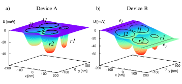
In the quasi-two-dimensional quadruple QD Shin079 , the confinement potential energy of the electron can be described by the following formula:
| (1) |
where , the QD’s are labelled by and (cf. Fig. 1), is the depth of the potential well (), is the range of the confinement potential that determines the size of QD, is the position of the center of QD, and parameter is responsible for the softness of the confinement potential KA09 . We consider two model nanodevices, denoted by A and B (Fig. 1). In nanodevice A [Fig. 1(a)], the confinement potential energy is given by Eq. (1) with variable potential-well depths , which can be tuned by changing the voltages applied to the nearby gates. In nanodevice B [Fig. 1 (b)], the confinement potential can be modified by switching on/off the bias voltage between electrodes and . Then, the electron gains the additional potential energy . Taking into account the finite range of electric field KA09 we put and at the right and left electrode, respectively, and in the region between the electrodes, where is the distance between electrodes and and . The total potential energy of the electron as a function of and is displayed in Figs. 1 and 2. In the initial state of the nanodevice, the electron potential energy of the left QD’s is set to be lower than that of the right QD’s (cf. Fig. 2).
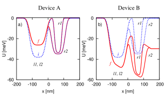
We have solved the Schrödinger equation for one and two electrons in the quadruple QD with the confinement potential energy (Fig. 1). For this purpose we have extended the method applied previously to the double QD KA09 . The two-electron problem has been solved by the configuration interaction method KA09 on a space grid with the one-electron wave functions obtained by the numerical variational method, described in Appendix of Ref. KA09 . The computational method KA09 provides accurate solutions to few-electron eigenproblems with an arbitrary confinement potential and electric field of finite range. The present calculations have been performed for the GaAs material parameters with donor rydberg meV and donor Bohr radius meV. The initial potential energy is characterized by meV, nm, meV, meV, meV, and meV. In the final state, meV for nanodevice A, while in nanodevice B, the potential energy is changed by the electric field kV/cm. The centers of QD’s are located at the vertices of the square that are lying at distance 127.3 nm from each other. The softness parameter is taken as [cf. Eq. (1)]. For each set of nanodevice parameters we have calculated the lowest singlet () and triplet () energy levels for the initial and final potential energy profiles (cf. Figs. 1 and 2). In the absence of magnetic field, the three triplet states () are degenerate, therefore, we are dealing with the triply degenerate level . We have also determined the localization of electrons in the QD’s for the lowest-energy and states by calculating the one-electron probability density KA09 .
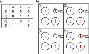
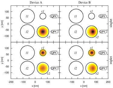
The localization of two electrons obtained for the initial and final potential profiles is schematically shown in Fig. 3 (b). Fig. 4 displays contours of the one-electron probability density calculated for the final potential profile (cf. Fig. 2). Fig. 4 shows that the electron distribution in the single QD possesses the rotational symmetry in nanodevice A and is slightly shifted towards the left contact in nanodevice B, which results from the effect of the homogeneous electric field. The results of Fig. 4 can be analyzed with the help of the truth table for the XOR logic gate [Fig. 3(a)]. The initial (input) state has been prepared so that the left QD’s are singly occupied by the electrons both in the singlet and triplet states. This electron localization is ensured by setting the potential wells of the left QD’s to be deeper than those of the right QD’s (cf. Fig. 2). We ascribe the logical values 0 and 1 to the initial spin states associated with the spin component and , respectively (Fig. 3). If we perform the controlled evolution of the electron states by slowly changing the potential energy profile (Fig. 2), the electrons become localized in the right QD’s (Fig. 4), since – in the final state – the potential wells of the right QD’s are considerably deeper than those of the left QD’s. The heights and thicknesses of energy barriers separating the QD’s have been chosen sufficiently large to prevent the tunnelling of electrons between QD and QD in the initial state. During the changes of the potential energy profile, the energy levels of the electrons confined in the left and right QD’s become equal to each other, which means that the resonant tunnelling conditions are satisfied, i.e., the electrons tunnel from the left to the right QD’s with the probability 1. The occupancy of the right QD’s is determined by the initial spin states of the electrons in the left QD’s. If we consider the QD, then – for the nanodevice parameters given above – this QD is occupied by either zero or one electron in the final state. Simultaneously, the QD is occupied by either two electrons or one electron. This occupancy can be detected by measuring charge of the QD by a sensitive charge detector, e.g., the quantum point contact schematically shown as QPC1 on Fig. 4. Alternatively, we can use the quantum point contact QPC2, placed near the QD, which measures charge of QD. The results of the present calculations allow us to predict the measurement outcomes. For both the nanodevices A and B, we obtain either or and either or for two different output charge states (Fig. 4). This means that both the nanodevices A and B operate as spin-charge converters. Moreover, these nanodevices can act as the XOR logic gates (Fig. 3). When measuring the charge of the single right QD, we can distinguish XOR logic operations (1) and (4) from operations (2) and (3) [Fig. 3(a)]. If we additionally know the initial electron spin states, we can uniquely determine each of the four XOR logic gate operations [Fig. 3(a)]. During operations (1-4) the input spin states of the left QD’s are transformed into the output charge states of the right QD’s.
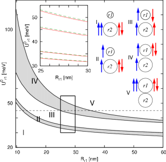
The nanodevices A and B can perform the XOR logic gate only for the suitably chosen nanodevice parameters. In order to determine the corresponding parameter regimes, we have performed many computational runs for different sets of parameters of QD keeping fixed the parameters of other QD’s. The localization of electrons in the right QD’s obtained for the final potential profile is schematically depicted in the right inset of Fig. 5. Fig. 5 shows that – based on the criterion of electron localization in the final state – we can distinguish five regimes, labelled by I through V, on the plane. In regime I, both the electrons are localized in the QD in either spin state. In regime II, we obtain the spin-dependent localization of the electrons in QD and QD. The nanodevices A and B with the parameters from regime II can operate as the XOR logic gates (cf. Fig. 4). In regime III, the electrons in each final spin state are localized in different QD’s. In regime IV, we recover the spin-dependent localization of the electrons in the right QD’s. Therefore, the nanodevices A and B with the parameters taking on the values from regime IV can perform the XOR logic gate operations. In comparison to regime II, the role of QD and QD is interchanged, which means that – in regime IV – the QPC2 will provide the same measurement outcomes as the QPC1 in regime II and vice versa. In regime V, both the electrons occupy the QD in each final spin state.
The left upper inset in Fig. 5 displays the zoom of the rectangular region on the main panel with the boundaries of regimes I-V obtained for nanodevices A and B. We observe that the boundaries of these parameter regimes change only slightly (these changes are of the order of the thickness of curves on the main panel). The smallness of these changes means that both the nanodevices A and B are essentially equivalent in the proposed realization of the XOR logic gate.
If the initial spin state is prepared as schematically shown in Fig. 3(b), i.e., the left QD’s are singly occupied by the electrons with either parallel or antiparallel spins, then the controlled quantum-state evolution performed by changing the electrostatic potential profile leads to the uniquely determined final quantum states of electrons. This occurs in all parameter regimes I-V (Fig. 5). In the final state, the electrons are localized in either one or two right QD’s in the well-defined spin states (cf. the right inset of Fig. 5). However, only in regimes II and IV, the localization of electrons in QD and QD depends on their spins. For the nanodevices A and B, characterized by the parameters from regimes II and IV, the measurements of the electric charge of either QD or QD allow us to distinguish the singlet and triplet final spin states (Fig. 4). Therefore, the nanodevices A and B can be used to the electrical readout of spin via the spin-to-charge conversion.
The present mechanism of the XOR logic gate is based on the results obtained for the stationary quantum states. In order to perform the controlled evolution between these states we have to apply the external electric field that appropriately modifies the electron potential energy. The electric field has to be switched on/off sufficiently slowly in order to cause the adiabatic transition from the initial to final state. The non-adiabatic transitions can lead to several spin flips during the quantum-state evolution, which makes the operation time longer Moskal07 . Nevertheless, the present mechanism leads to the realization of the XOR gate, if the spins of electrons are the same in the initial and final states [cf. Fig. 3(b)]. The electrons only change their localization as a result of tunnelling from the left to right QD’s. Therefore, the XOR gate operation time may be short enough in order to perform the sufficiently large number of operations during the spin coherence time Hans03 .
We note that the two-qubit XOR logic gate is commonly defined as follows: , where is the addition modulo two. This two-qubit XOR gate is equivalent to the CNOT gate DiV98 . However, according the present mechanism, the nanodevices A and B perform the following operation: , where , and are defined in Fig. 3(a) and the output is detected by QPC1 as the charge of QD (cf. Fig. 4). If we alternatively apply the QPC2 to measure the charge of QD, then the final charge state is also uniquely determined by the input spin states of the left QD’s. Therefore, the logic gate studied in this Letter possesses all the properties of the XOR gate defined in Fig. 3(a). The logic gate operations realized in nanodevices A and B result from the quantum transitions between the well-defined quantum states of the electrons. During these operations, the input spin qubits are transformed into the output charge qubits by changing the external voltages, i.e., by the all-electrical control. The nanodevices A and B can realize the entire cycle of the XOR logic gate, i.e., the input state preparation, electrically driven evolution of quantum states, and readout of the output via the spin-to-charge conversion. The XOR logic gate, proposed in this Letter, can be realized in the quadruple QD’s recently studied by Shinkai et al. Shin079 .
In summary, we have proposed the all-electrical implementation of the XOR logic gate in two nanodevices based on the laterally coupled quadruple QD’s.
Acknowledgements.
This paper has been partly supported by the Polish Scientific Network LFPPI ”Laboratory of Physical Fundamentals of Information Processing”.References
- (1) G. Burkard et al., Phys. Rev. B 59, 2070 (1999).
- (2) T. Hayashi el al., Phys. Rev. Lett. 91, 226804 (2003).
- (3) J.M. Elzerman et al., Phys. Rev. B 67, 161308(R) (2003); Nature 430, 431 (2004).
- (4) S. Sangu et al., Phys. Rev. B 69, 115334 (2004).
- (5) J.R. Petta et al., Science 309, 2180 (2005).
- (6) R. Hanson et al., Phys. Rev. Lett. 94, 196802 (2005).
- (7) P. Hawrylak and M. Korkusinski, Solid State Commun. 136, 508 (2005); M. Korkusinski et al., Phys. Rev. B 75, 115301 (2007).
- (8) T. Meunier et al., Phys. Rev. B 74, 195303 (2006).
- (9) S. Sauvage et al., Phys. Rev. Lett. 88, 177402 (2002).
- (10) R. Hanson et al., Phys. Rev. Lett. 91, 196802 (2003).
- (11) J. Adamowski et al., Handbook of Semiconductor Nanostructures and Nanodevices, Vol. 1, ed. A.A. Balandin and K.L. Wang (CA: American Scientific Publishers), p. 389 (2006).
- (12) M. Stopa et al., Physica E 34, 616 (2006).
- (13) Z. Jiang et al., Phys. Rev. B 78, 035307 (2008).
- (14) G. Shinkai et al., Appl. Phys. Lett. 90, 103116 (2007); cond-mat arXiv: 0905.0805v2.
- (15) A. Barenco et al., Phys. Rev. A 52, 3457 (1995).
- (16) S. Bednarek and B. Szafran, Phys. Rev. Lett. 101, 216805 (2008); Nanotechnology 20, 065402 (2009).
- (17) S. Moskal et al., Phys. Rev A 71, 062327 (2005).
- (18) A. Kwaśniowski and J. Adamowski, J.Phys.: Condens. Matter 21, 235601 (2009).
- (19) S. Moskal et al., Phys. Rev A 76, 032302 (2007).
- (20) D.P. DiVincenzo, Proc. R. Soc. London A 454, 261 (1998).