Surface decorated silicon nanowires: a route to high-ZT thermoelectrics
Abstract
Based on atomistic calculations of electron and phonon transport, we propose to use surface decorated Silicon nanowires (SiNWs) for thermoelectric applications. Two examples of surface decorations are studied to illustrate the underlying ideas: Nanotrees and alkyl functionalized SiNWs. For both systems we find, (i) that the phonon conductance is significantly reduced compared to the electronic conductance leading to high thermoelectric figure of merit, , and (ii) for ultra-thin wires surface decoration leads to significantly better performance than surface disorder.
pacs:
63.22.Gh, 72.15.Jf, 73.63.-b, 66.70.-fRecent ground-breaking experiments indicate that rough silicon nanowires (SiNWs) can be efficient thermoelectric materials although bulk silicon is not Hochbaum et al. (2008); Boukai et al. (2008): they conduct charge well but have a low heat conductivity. A measure for the performance is given by the figure of merit , where , , and , are the electrical conductance, Seebeck coefficient, and (average) temperature, respectively. The heat conduction has both electronic and phononic contributions, . Materials with are regarded as good thermoelectrics, but is required to compete with conventional refrigerators or generators Marjumdar (2004). Recent theoretical works predict in ultra-thin SiNWs Vo et al. (2008); Ramayya et al. (2008); Markussen et al. (2009). The high performance SiNWs in Ref. Hochbaum et al. (2008) were deliberately produced with a very rough surface, and the high is attributed to increased phonon-surface scattering which decreases the phonon heat conductivity, while the electrons are less affected by the surface roughness. The extraordinary low thermal conductivity measured in rough SiNWs is supported be recent calculations Martin et al. (2009); Donadio and Galli (2009). Surface disorder will, however, begin to affect the electronic conductance significantly in very thin wires Persson et al. (2008) and thereby reduce Ramayya et al. (2008); Markussen et al. (2009).
For defect-free wires, the room temperature phononic conductance scales with the cross-sectional area Markussen et al. (2008). Contrary, for ultra-thin wires with diameters nm, the electronic conductance is not proportional to the area: it is quantized and given by the number of valence/conduction band states at the band edges. Decreasing the diameter to this range thus decreases while keeping almost constant. An optimally designed thermoelectric material would scatter phonons but leave the electronic conductance unaffected, even for the smallest wires. Instead of introducing surface disorder, which affects the electronic conductance in the thin wires, it is interesting to speculate whether other surface designs could lead to improved thermoelectric performance. Lee et al. Lee et al. (2008) proposed nanoporous Si as an efficient thermoelectric matrial. Blase and Fernández-Serra Blase and Fernández-Serra (2008) recently showed that covalent functionalization of SiNW surfaces with alkyl molecules leaves the electronic conductance unchanged, because the molecular states are well separated in energy from the nanowire bandedges, see Fig. 1. If the alkyl molecules scatter the phonons, such functionalized SiNWs would be candidates for thermoelectric applications. Experimental alkyl functionalization of SiNWs was reported in Ref. Haick et al. (2006).
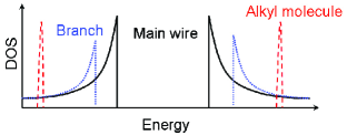
Another possible surface design are branched SiNWs, so-called nanotrees. Nanotrees have been synthesized in III-VI semiconductors Dick et al. (2004a, b) and in silicon Fonseca et al. (2005); Doerk et al. (2008). The stability and electronic structure of silicon nanotrees have recently been addressed theoretically Menon et al. (2007); Avramov et al. (2007). The thinner branches will have a larger band gap than the main wire (”trunk”), see Fig. 1. Close to the band edges, the electronic scattering is therefore weak.
The presence of an alkyl molecule or a nanowire branch leads both to a reduction, , of the thermal conductance and a reduction, , of the electronic conductance. In this letter we show that at room temperature (RT) the ratio for the alkyl functionalized SiNWs, and for a nanotree. By engineering the SiNW surfaces it is thus possible to reduce the phonon conductance while keeping the electronic conductance almost unaffected. We thus propose such surface decorated SiNWs as promising candidates for nanoscale thermoelectric applications.
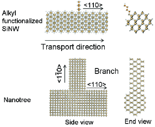
Systems. We consider two specific systems shown in Fig. 1. The first is an alkyl functionalized SiNW with a wire diameter of 12 Å, and with the wire oriented along the direction. The alkyl (CnH2n+1) is attached to the H-passivated nanowire replacing a H atom. The second system is a nanotree, where a small diameter (12 Å) branch is attached to a larger diameter (20 Å) trunk. The trunk is oriented in the direction while the branch is oriented along the direction, and is thus perpendicular to the trunk. The length of the branch, , is varied.
Methods. The electronic Hamiltonian, , and overlap matrix, , of the alkyl functionalized SiNWs are obtained from local orbital DFT calculations Soler et al. (2002); aa (2009). The calculations are performed on super-cells containing 7 wire unit cells with the alkyl molecule bound to the middlemost unit cell, as shown in Fig. 1.
For the nanotrees, we use a tight-binding (TB) model since these systems contain atoms, too many for our DFT implementation. The electronic TB Hamiltonian describing the nanotree is calculated using a 10 band nearest-neighbor orthogonal TB parametrization Boykin et al. (2004); Zheng et al. (2005). We recently applied the same TB model to study thermoelectric properties of surface disordered SiNWs Markussen et al. (2009).
The phononic system, characterized by the force constant matrix, , is described using the Tersoff empirical potential (TEP) model Tersoff (1988, 1989) for both the nanotree and the functionalized SiNW. For pristine wires, we have recently shown that the TEP model agrees well with more elaborate DFT calculations Markussen et al. (2008). We limit our description to the harmonic approximation, thus neglecting phonon-phonon scattering. The harmonic approximation is always valid at low temperatures. In bulk Si, the room temperature anharmonic phonon-phonon relaxation length at the highest frequencies is nm and increases as at lower frequencies Mingo and Yang (2003). Experimental studies of silicon films Ju and Goodson (1999) showed that the effective mean free path of the dominant phonons at room temperature is 300 nm. For relatively short wires with lengths nm the anharmonic effects thus seem to be of limited importance, and the harmonic approximation is expected to be good.
We calculate the electronic conductance from the electronic transmission function, . This is obtained from the -matrices following the standard non-equilibrium Green’s function (NEGF)/Landauer setup, where the scattering region (i.e. the regions shown in Fig. 1) is coupled to semi-infinite, perfect wires Haug and Jauho (2008). The electronic quantities in the formula can be written as Sivan and Imry (1986); Esfarjani et al. (2006); Lunde and Flensberg (2005) , and where is given by
| (1) |
Here is the Fermi-Dirac distribution function at the chemical potential .
The phonon transmission function, , at frequency is calculated in a similar way as the electronic transmission with the substitutions and , where is a diagonal matrix with the atomic masses Yamamoto and Watanabe (2006); Mingo (2006); Wang et al. (2006). The phonon thermal conductance is
| (2) |
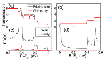

Charge transport. Figures 2 (a) and (b) show the calculated hole and electron transmissions for a pentyl (C5H11) functionalized SiNW. Notably, the transmission is nearly perfect close to the bandedges. The average reduction of the transmission in the first hole and electron conductance plateaus are 2% and 0.2%, respectively, in agreement with the findings of Ref. Blase and Fernández-Serra (2008). Figures 2 (c) and (d) show the projected density of states (PDOS) on the wire and on the pentyl. The high transmission regions in panel (a) and (b) are seen to correspond with regions of vanishing PDOS on the pentyl molecule. Likewise, at energies in the valence band where scattering is observed, there is a relatively large PDOS at the pentyl.
Figures 2 (e) and (f) show the transmission through the nanotree. The branch length is Å. Again, the transmission close to the band edges is nearly perfect, with a reduction of 2% and 0.9% for holes and electrons, respectively. Figures 2 (g) and (h) show the PDOS on the main wire and on the branch. We again observe a correspondence between perfect transmission and low PDOS on the branch.
The almost perfect transmissions close to the band edges can be qualitatively understood from the schematic drawing in Fig. 1 (top). The HOMO and LUMO level of the pentyl are located deep inside the bands Blase and Fernández-Serra (2008) and the molecular states are thus not accessible for electrons or holes close to the band edges. For the nanotree, the branch has a smaller diameter and thus a larger bandgap. Electrons or holes in the trunk, with energies close to the band edges, are not energetically allowed in the branch and therefore do not ’see’ the branch. In addition to the energy considerations, the spatial distribution of the Bloch state also plays a role: the first valence and conduction band Bloch states of the main wire have more weight in the center of the wire than at the edge Markussen et al. (2009).
Thermal transport. Figure 3 shows the temperature dependence of the thermal conductance ratios , where is the pristine wire thermal conductance, which in the low energy limit equals the universal thermal conductance quantum, Schwab et al. (2000). Panel (a) shows the ratios for wires with alkyles, CnH2n+1, with different lengths, . The thermal conductance at RT is reduced by %, and the overall behavior does not depend on the alkyl length. The inset shows the phonon transmission at low phonon energies. Note the resonant dips in the transmission, where exactly one channel is closed yielding a transmission of three. These dips are associated with an increased local phonon density of states at the alkyl molecule at the resonant energies, corresponding to a localized vibrational mode. Such Fano-like resonant scattering is well-known from electron transport Nockel and Stone (1994). A phonon eigenchannel analysis Paulsson and Brandbyge (2007) shows that the transmission dips are due to a complete blocking of the rotational mode in the wire. The corresponding localized alkyl phonon mode is a vibration in the plane perpendicular to the wire axis.
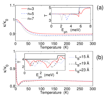
Panel (b) in Fig. 3 shows the thermal conductance ratio for nanotrees with different branch length, . There is only a weak dependence on at low temperatures, and at RT the four curves basically coincide showing a thermal conductance reduction of 17% of the nanotree compared to the pristine wire. Again we observe resonant transmission dips for the nanotrees. Two channels - the rotational and one flexural mode - close completely at the resonance due to two quasi-localized vibrational modes in the branch. These phonon backscattering resonances are responsible for the dip in the ratio around K. Notice that all the conductance ratios approach unity in the low temperature limit. This is because the four acoustic modes transmit perfectly in the limit Schwab et al. (2000).
We may vary the thermoelectric figure of merit, , by varying the chemical potential. Typically displays a maximum for close to the band edge Markussen et al. (2009); Vo et al. (2008). Figure 4 shows the maximum values for the pentyl functionalized SiNW (squares), the nanotree (circles), and surface disordered SiNWs (triangles), where disorder is modeled by introducing surface silicon vacancies. The diameter of the surface disordered wire is Å and it is oriented along the direction. The calculational details are given in Ref. Markussen et al. (2009). The curves show as a function of the number () of pentyl molecules/nanotree branches/silicon vacancies. In calculating vs , we have assumed that the transmission, , through a longer wire with e.g. pentyl molecules randomly covering the surface can be obtained from the single-pentyl transmission, as , where is the pristine wire transmission. The term in parenthesis corresponds to a scattering resistance of a single pentyl molecules. This averaging method has recently been validated in the quasi-ballistic and diffusive regimes for both electron and phonon transport Markussen et al. (2009); Savić et al. (2008); Markussen et al. (2007).
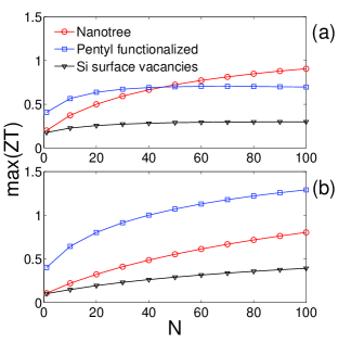
Figure 4 shows that increasing the number of scattering centers, i.e. the number of pentyl molecules or nanotree branches increases the for both hole transport (a) and electron transport (b). In the case of holes in the pentyl functionalized SiNWs, the reaches an almost constant level of at , but in all other cases, increases throughout the range. Increasing the density of molecules/nanotree branches or increasing the length of the wire will thus increase the thermoelectric performance. The reason is that the electrons (holes) are less affected by the surface modifications than the phonons, as also seen in Figs. 2 and 3. The surface disordered wires (triangles) show an increasing vs but at values significantly lower than the two other surface modified wires.
Discussion. A number of idealizations have been made in our calculations, and we next assess their significance. The structures we have considered represent plausible choices, dictated by computational limitations, but do not necessarily match quantitatively real structures. Thus, for example, a surface decorated SiNW will also be rough, and one should consider the combined effect of all scattering mechanisms. We have not carried out optimizations neither with respect to the attached molecules nor with respect to the geometry of the nanotrees. Electron-phonon and phonon-phonon scattering will affect both the electronic and thermal conductances and the obtained values Ramayya et al. (2008). We do not expect to reach quantitative agreement with experiment but believe to have identified important trends: In SiNW based thermoelectrics, surface decorations in terms of added molecules or nanowire branches seem to be a better approach than surface disorder in the ultra-thin limit.
We thank the Danish Center for Scientific Computing (DCSC) and Direktør Henriksens Fond for providing computer resources. TM acknowledges the Denmark-America foundation for financial support. APJ is grateful to the FiDiPro program of the Finnish Academy.
References
- Hochbaum et al. (2008) A. Hochbaum, R. Chen, R. D. Delgado, W. Liang, E. C. Garnett, M. Najarian, A. Marumdar, and P. Yang, Nature 451, 163 (2008).
- Boukai et al. (2008) A. I. Boukai, Y. Bunimovich, J. Tahir-Kheli, J.-K. Yu, W. A. Goddard III, and J. R. Heath, Nature 451, 168 (2008).
- Marjumdar (2004) A. Marjumdar, Science 303, 777 (2004).
- Vo et al. (2008) T. T. M. Vo, A. J. Williamson, V. Lordi, and G. Galli, Nano Lett. 8, 1111 (2008).
- Ramayya et al. (2008) E. Ramayya, D. Vasileska, S. Goodnick, and I. Knezevic, Nano 08, 8th IEEE Conference on Nanotechnology, 339–342 (2008).
- Markussen et al. (2009) T. Markussen, A.-P. Jauho, and M. Brandbyge, Phys. Rev. B 79, 035415 (2009).
- Martin et al. (2009) P. Martin, Z. Aksamija, E. Pop, and U. Ravaioli, Phys. Rev. Lett. 102, 125503 (2009).
- Donadio and Galli (2009) D. Donadio and G. Galli, Phys. Rev. Lett. 102, 195901 (2009).
- Persson et al. (2008) M. P. Persson, A. Lherbier, Y.-M. Niquet, F. Triozon, and S. Roche, Nano Lett. 8, 4146–4150 (2008).
- Markussen et al. (2008) T. Markussen, A.-P. Jauho, and M. Brandbyge, Nano Lett. 8, 3771 (2008).
- Lee et al. (2008) J.-H. Lee, G. A. Galli, and J. C. Grossman, Nano Letters 8, 3750 (2008).
- Blase and Fernández-Serra (2008) X. Blase and M.-V. Fernández-Serra, Phys. Rev. Lett. 100, 046802 (2008).
- Haick et al. (2006) H. Haick, P. T. Hurley, A. I. Hochbaum, P. Yang, and N. S. Lewis, J. Am. Chem. Soc. 128, 8990 (2006).
- Dick et al. (2004a) K. A. Dick, K. Deppert, T. Martensson, W. Seifert, and L. Samuelson, J. Cryst. Growth 272, 131 (2004a).
- Dick et al. (2004b) K. A. Dick, K. Deppert, M. W. Larsson, T. Martensson, W. Seifert, L. R. Wallenberg, and L. Samuelson, Nat. Mater. 3, 380 (2004b).
- Fonseca et al. (2005) L. Fonseca, O. Resto, and F. Sola, Appl. Phys. Lett. 87, 113111 (2005).
- Doerk et al. (2008) G. S. Doerk, N. Ferralis, C. Carraro, and R. Maboudian, J. Mat. Chem. 18, 5376 (2008).
- Menon et al. (2007) M. Menon, E. Richter, I. Lee, and P. Raghavan, J. Comput. Theor. Nanosci. 4, 252 (2007).
- Avramov et al. (2007) P. V. Avramov, L. A. Chernozatonskii, P. B. Sorokin, and M. S. Gordon, Nano Lett. 7, 2063 (2007).
- Soler et al. (2002) J. M. Soler, E. Artacho, J. D. Gale, A. García, J. Junquera, P. Ordejón, and D. Sánchez-Portal, J. Phys.: Condens. Matter 14, 2745 (2002).
- aa (2009) We use a single- polarized basis set with an energy cutoff of 200 Ry, norm-conserving pseudopotentials and the generalized-gradient approximation for the exchange-correlation functional.
- Boykin et al. (2004) T. B. Boykin, G. Klimeck, and F. Oyafuso, Phys. Rev. B 69, 115201 (2004).
- Zheng et al. (2005) Y. Zheng, C. Riva, R. Lake, K. Alam, T. B. Boykin, and G. Klimeck, IEEE Trans. Electron Devices 52, 1097 (2005).
- Tersoff (1988) J. Tersoff, Phys. Rev. B 38, 9902 (1988).
- Tersoff (1989) J. Tersoff, Phys. Rev. B 39, 5566 (1989).
- Mingo and Yang (2003) N. Mingo and L. Yang, Phys. Rev. B 68, 245406 (2003).
- Ju and Goodson (1999) Y. S. Ju and K. E. Goodson, Appl. Phys. Lett. 74, 3005 (1999).
- Haug and Jauho (2008) H. Haug and A.-P. Jauho, Quantum Kinetics in Transport and Optics of Semiconductors, vol. 123 of Springer Solid State Series (Springer, 2008), 2nd ed.
- Sivan and Imry (1986) U. Sivan and Y. Imry, Phys. Rev. B 33, 551 (1986).
- Esfarjani et al. (2006) K. Esfarjani, M. Zebarjadi, and Y. Kawazoe, Phys. Rev. B 73, 085406 (2006).
- Lunde and Flensberg (2005) A. M. Lunde and K. Flensberg, J. Phys.: Condens. Matter 17 (2005).
- Yamamoto and Watanabe (2006) T. Yamamoto and K. Watanabe, Phys. Rev. Lett. 96, 255503 (2006).
- Mingo (2006) N. Mingo, Phys. Rev. B 74, 125402 (2006).
- Wang et al. (2006) J.-S. Wang, J. Wang, and N. Zeng, Phys. Rev. B 74, 033408 (2006).
- Schwab et al. (2000) K. Schwab, E. A. Henriksen, J. M. Worlock, and M. L. Roukes, Nature 404, 974 (2000).
- Nockel and Stone (1994) J. U. Nockel and A. D. Stone, Phys. Rev. B 50, 17415 (1994).
- Paulsson and Brandbyge (2007) M. Paulsson and M. Brandbyge, Phys. Rev. B 76, 115117 (2007).
- Savić et al. (2008) I. Savić, D. A. Stewart, and N. Mingo, Phys. Rev. B 78, 235434 (2008).
- Markussen et al. (2007) T. Markussen, R. Rurali, A.-P. Jauho, and M. Brandbyge, Phys. Rev. Lett. 99, 076803 (2007).