Surface electromagnetic phenomena in pristine and atomically doped carbon nanotubes
Abstract
The article reviews recent progress in the theoretical understanding of near-field surface electromagnetic phenomena in pristine and atomically doped carbon nanotubes. The phenomena involving strong coupling effects are outlined. They are the optical absorption by single-walled carbon nanotubes doped with single atoms or ions in the frequency range close to the atomic transition frequency, the entanglement of the pair of atomic qubits strongly coupled to a common high-finesse surface photonic mode of the nanotube, and the optical response of the strongly coupled surface exciton-plasmon excitations in pristine semiconducting carbon nanotubes. The phenomena reviewed have a great potential to be exploited for the future development of the nanotube based tunable optoelectronic device applications in areas such as nanophotonics, nanoplasmonics, cavity quantum electrodynamics, and quantum information science.
pacs:
78.40.Ri, 73.22.-f, 73.63.Fg, 78.67.Ch1. Introduction
Single-walled carbon nanotubes (CNs) are quasi-one-dimensional (1D) cylindrical wires consisting of graphene sheets rolled-up into cylinders with diameters nm and lengths m Dresselhaus ; Dai ; Zheng ; Huang . Nanotubes are shown to be useful as miniaturized electronic, electromechanical, and chemical devices Baughman , scanning probe devices Popescu , and nanomaterials for macroscopic composites Trancik . Their intrinsic physical properties may be substantially modified in a controllable way by doping with extrinsic impurity atoms, molecules and compounds Latil ; Son ; Duclaux ; Shimoda ; Jeong ; Jeongtsf ; Khazaei .
Recent successful experiments on the encapsulation of single atoms into single-walled CNs Jeong ; Jeongtsf ; Khazaei and their intercalation into single-wall CN bundles Duclaux ; Shimoda , along with the numerous previous studies of monoatomic gas absorption by the nanotube bundles (see, e.g., Ref. Calbi ) and the progress in growth techniques of centimeter-long small-diameter single-walled carbon nanotubes Zheng ; Huang , stimulated an in-depth theoretical analysis of dynamic quantum coherent processes in CNs doped with single atoms or ions. As a result, atomically doped nanotubes have been recently demonstrated to be very efficient as applied to nanophotonics, cavity quantum electrodynamics (QED) and quantum communication Bondarev06 ; Bondarev07 ; Bondarev07jem ; Bondarev07os .
For pristine (undoped) single-walled CNs, the numerical calculations predicting large exciton binding energies ( eV) in semiconducting CNs Pedersen03 ; Pedersen04 ; Capaz and even in some small-diameter ( nm) metallic CNs Spataru04 , followed by the results of various exciton photoluminescence measurements Imamoglu ; Wang04 ; Wang05 ; Hagen05 ; Plentz05 ; Avouris08 , have become available. These works, together with other reports investigating the role of effects such as intrinsic defects Hagen05 ; Prezhdo08 , exciton-phonon interactions Plentz05 ; Prezhdo08 ; Perebeinos05 ; Lazzeri05 ; Piscanec , exciton-surface-plasmon coupling Bondarev08 ; Bondarev09 , effects of external magnetic Zaric ; Srivastava and electric fields Perebeinos07 , reveal the variety and complexity of the intrinsic optical properties of semiconductor carbon nanotubes Dresselhaus07 . At the same time, they pave the way for the novel applications of carbon nanotubes in modern optoelectronics in areas such as various aspects of photophysics, nanoplasmonics, and quantum information science, which are essentially beyond relatively well explored nanoelectronics and nanoelectromechanics with carbon nanotubes. For instance, recent experimental observations of quantum correlations in the photoluminescence spectra of individual CNs suggest their potential applicability in quantum cryptography Imamoglu .
In spite of impressive experimental demonstrations of basic quantum information effects in a number of different nanoscale solid state systems, such as quantum dots in semiconductor microcavities, nuclear spin systems, Josephson junctions, etc., their concrete implementation is still at the proof-of-principle stage (see, e.g., Ref. Brandes for a review). The development of materials that may host quantum coherent states with long coherence lifetimes is a critical research problem for the nearest future. There is a need for the fabrication of quantum bits (qubits) with coherence lifetimes at least three-four orders of magnitude longer than it takes to perform a bit flip Brandes ; Lukin ; Benjamin . To achieve this goal, a critical prerequisite of the strong coupling of an atomic, excitonic or intersubband electronic transition to a high-finesse vacuum-type electromagnetic mode of its environment (e.g., a semiconductor optical microcavity mode) needs to be fulfilled. Under strong coupling, new elementary excitations, the eigen states of the full photon-matter Hamiltonian, form. They are so-called ’cavity polaritons’ representing a characteristic anticrossing behavior with a mode separation often referred to as ’vacuum-field Rabi splitting’. A pair of the cavity polaritons (term used in a broad sense here) coupled to the same high-finesse vacuum-type electromagnetic mode of the surrounding material would involve polariton entangling operations Bondarev07 ; Lukin ; Benjamin ; Hughes ; Cirac , followed by the nearest neighbor interaction over short distances and quantum information transfer over longer distances.
For atomically doped carbon nanotubes, there may be typically two qualitatively different regimes of the interaction of an atomic state with the medium-assisted surface electromagnetic modes of a CN Bondarev02 ; Bondarev04 ; Bondarev04pla ; Bondarev05 ; Bondarev04ssc ; Bondarev06trends . They are the weak coupling regime and the strong coupling regime. The former is characterized by the monotonic exponential decay dynamics of the upper atomic state with the decay rate altered compared to the free-space value due to the presence of the additional decay modes associated with the presence of the nanotube. The latter is, in contrast, strictly non-exponential and is characterized by the reversible (Rabi) oscillations where the energy of the initially excited atom is periodically exchanged between the atom and the surface electromagnetic mode of the nanotube. The strong coupling regime was shown recently to occur in small-diameter ( nm) atomically doped CNs with the atomic transition tuned to the resonance (representing the field mode) of the local density of the nanotube’s surface photonic states (DOS) Bondarev04 ; Bondarev04pla ; Bondarev05 ; Bondarev04ssc ; Bondarev06trends . This result can be qualitatively understood in terms of the cavity QED. The coupling constant of an atom (modelled by a two-level system with the transition dipole moment and frequency ) to a local vacuum-type field is given by with being the effective volume of the field mode the atom interacts with (see, e.g., Ref. Andreani ). For the atom (ion) encapsulated into the CN of radius , the local field mode volume is estimated to be that is nm3 for CNs with diameters nm in the optical range of nm. Approximating Davydov , one obtains eV. On the other hand, the ”cavity” linewidth is given for in resonance with the cavity mode by , where is the atomic spontaneous emission enhancement/dehancement (Purcell) factor Andreani . Taking into account large Purcell factors close to CNs Bondarev02 , one arrives at eV for 1 nm-diameter CNs in the optical spectral range. Thus, for the atoms (ions) encapsulated into the small-diameter CNs the strong atom-field coupling condition is fulfilled, giving rise to the rearrangement (”dressing”) of the atomic levels followed by the formation of quasi-one-dimensional (1D) atomic cavity polaritons Bondarev04 ; Bondarev04pla ; Bondarev05 ; Bondarev04ssc ; Bondarev06trends . The latter ones are similar to quasi-0D excitonic polaritons in quantum dots in semiconductor microcavities Reithmaier ; Yoshie ; Peter , which are theoretically proposed to be a way to produce the excitonic states entanglement for use in solid state quantum information science applications Hughes . Similar way to entangle the pair of spatially separated quasi-1D atomic polaritons in metallic small-diameter single-walled CNs has been theoretically demonstrated to be feasible as well Bondarev07 . It is important to pursue a variety of different strategies and approaches towards physically implementing novel non-trivial applications in modern nanotechnology.
For pristine small-diameter ( nm) semiconducting single-walled CNs, the exciton-surface-plasmon interactions have been shown recently to result in the strong exciton-plasmon coupling regime Bondarev08 ; Bondarev09 . This is due to the fact that the low-energy weakly-dispersive interband plasmon modes (resulted from the transverse quantization of the electronic motion on the nanotube surface — observed in Ref. Pichler98 ) occur in the same energy range of eV where the lowest exciton excitation energies are located in small-diameter CNs Spataru05 ; Ma . Previous studies of the exciton-plasmon interactions in nanomaterials have been focused on artificially fabricated hybrid plasmonic nanostructures, such as dye molecules in organic polymers deposited on metallic films Bellessa , semiconductor quantum dots coupled to metallic nanoparticles Govorov , or nanowires Fedutik , where one material carries the exciton and another one carries the plasmon. The effect of the strong exciton-plasmon coupling in CNs is particularly interesting since here the fundamental electromagnetic phenomenon of strong coupling occurs in an individual quasi-1D nanostructure, a carbon nanotube.
This article briefly reviews recent progress in the theoretical understanding of near-field surface electromagnetic phenomena in pristine and atomically doped CNs. It focuses on the phenomena that involve the strong coupling effects. Specifically, light absorption by atomically doped CNs and the entanglement of spatially separated strongly coupled quasi-1D atomic polaritons are discussed. Also, physical reasons for the exciton-surface-plasmon coupling in pristine small-diameter semiconducting CNs is given, and the optical response of the strongly coupled surface exciton-plasmon excitations is analyzed. These strong coupling phenomena have a great potential to be exploited for the future development of the nanotube based tunable optoelectronic device applications in areas such as nanophotonics, nanoplasmonics, cavity QED, and quantum information science.
The macroscopic electromagnetic Green function formalism is used throughout the paper, developed in Refs. Bondarev02 ; Bondarev04 ; Bondarev04pla ; Bondarev04ssc ; Bondarev05 ; Bondarev06trends to study the quantum nature of the near-field electromagnetic interactions in quasi-1D nanostructures featuring strong absorption. The formalism follows the original line of the macroscopic QED approach introduced by Welsch and coworkers to rigorously describe medium-assisted electromagnetic vacuum effects in dispersing and absorbing media VogelWelsch ; ScheelWelsch ; BuhmannWelsch (and refs. therein).
The paper is organized as follows. Section 2 analyzes the optical absorption by single-walled CNs doped with single atoms (or ions) in the frequency range close to the atomic transition frequency. A significant line (Rabi) splitting effect is demonstrated for small-diameter ( nm) CNs Bondarev06 , which indicates the strong atom-field coupling regime known to facilitate the entanglement of spatially separated atomic qubits Cirac ; Dung . Section 3 calculates the entanglement of formation for the pair of atomic qubits (quasi-1D atomic polaritons) strongly coupled to the same medium-assisted high-finesse surface photon mode of the nanotube. Small-diameter metallic nanotubes are shown to result in sizable amounts of the two-qubit atomic entanglement for sufficiently long times Bondarev07 . Section 4 describes the physical nature of the interactions between excitonic states and interband surface plasmons in pristine small-diameter semiconducting single-walled CNs, and calculates the optical response (exciton absorption) under strong exciton-plasmon coupling. Section 5 discusses the envisaged nanotube based applications of the phenomena considered, summarizes and concludes the article.
2. Optical Absorbtion by Atomically Doped CNs
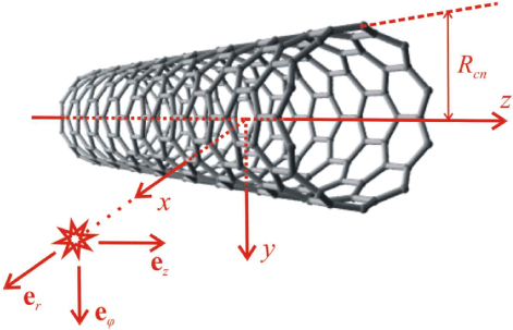
The (achiral) CN is modelled by an infinitely long, infinitely thin, anisotropically conducting cylinder. Its (axial) surface conductivity is taken to be that given by the -electron band structure in the tight-binding approximation with the azimuthal electron momentum quantization and axial electron momentum relaxation taken into account. A two-level atom is positioned at the point near an infinitely long achiral single-wall CN (Fig. 1). The orthonormal cylindric basis is chosen in such a way that is directed along the nanotube axis and, without loss of generality, . The atom interacts with the quantum electromagnetic field via its transition dipole moment directed along the CN axis, . The contribution of the transverse dipole moment orientations is suppressed because of the strong depolarization of the transverse field in an isolated CN Benedict ; Tasaki ; Li ; Marinop ; Ando ; Kozinsky . Under these assumptions, the photon Green function formalism developed earlier in Refs. Bondarev05 ; Bondarev06trends for quantizing an electromagnetic field close to quasi-1D absorbing and dispersing media generates the total second quantized Hamiltonian (Gaussian units)
| (1) | |||
where the three terms represent the medium-assisted (modified by the presence of the CN) electromagnetic field, the two-level atom and their interaction, respectively. The operators and are the scalar bosonic field operators defined on the CN surface assigned by the radius-vector with being the radius of the CN. These operators create and annihilate the single-quantum bosonic-type electromagnetic medium excitation of the frequency at the point of the CN surface. The Pauli operators, , and , describe the atomic subsystem and electric dipole transitions between the two atomic states, upper and lower , separated by the transition frequency . This (bare) frequency is modified by the diamagnetic () atom-field interaction yielding the new renormalized frequency
in the second term of the Hamiltonian. The dipole atom-field interaction matrix elements are given by , where
with being the -component of the transverse (longitudinal) Green tensor (with respect to the first variable) of the electromagnetic subsystem, and representing the CN surface axial conductivity. The matrix elements have the property of
with
being the transverse (longitudinal) distance-dependent (local) photonic DOS functions, and
representing the atomic spontaneous decay rate in vacuum, where is the vacuum imaginary Green tensor -component.
The Hamiltonian (1) involves only two standard approximations. They are the electric dipole approximation and the two-level approximation. The rotating wave approximation commonly used is not applied, and the diamagnetic term of the atom-field interaction is not neglected (as opposed to, e.g., Refs. Bondarev02 ; Bondarev04 ; Bondarev04pla ; Dung ). Quantum electrodynamics of the two-level atom (ion) close to the CN is thus described in terms of only two intrinsic characteristics of the electromagnetic subsystem — the transverse and longitudinal local photonic DOS functions.
When the atom is initially in the upper state and the field subsystem is in vacuum, the time-dependent wave function of the whole system can be written as
| (2) | |||
where is the vacuum state of the field subsystem, is its excited state with the field being in the single-quantum Fock state, and are the population probability amplitudes of the upper state and the lower state of the whole system, respectively. Applying the Hamiltonian (1) to the wave function (2), one has
| (3) | |||
| (4) |
In terms of the probability amplitudes above, the emission/absorbtion spectral line shape is given by Heitler . (Obviously, the absorbtion line shape coincides with the emission line shape if the monochromatic incident light beam is used in the absorbtion experiment.) This, after the substitution of obtained by the integration [under initial conditions , ] of Eq. (4), yields in dimensionless variables
| (5) |
where
with eV being the carbon nearest neighbor hopping integral ( s) appearing in the CN surface axial conductivity , and
The upper state population probability amplitude in Eq. (5) is given by the Volterra integral equation [obtained by substituting the result of the formal integration of Eq. (4) into Eq. (3)] with the kernel determined by the local photonic DOS functions Bondarev05 ; Bondarev04ssc ; Bondarev06trends . Thus, the numerical solution is only possible for the line shape , strictly speaking. This, however, offers very little physical insight into the problem of the optical absorbtion by atomically doped CNs under different atom-field coupling regimes. On the other hand, for those atomic transition frequencies which are located in the vicinity of the resonance frequencies of the DOS functions a simple analytical approach may be applied. Specifically, can be approximated by the Lorentzians of the same half-width-at-half-maxima , thus making it possible to solve the integral equation for analytically to obtain Bondarev04 ; Bondarev04pla ; Bondarev06trends
| (6) | |||
with
| (7) |
This solution is valid for whatever the atom-field coupling strength is, yielding the exponential decay of the upper state population, with the rate , in the weak coupling regime where , and the decay via damped Rabi oscillations, , in the strong coupling regime where .
Substituting Eq. (6) into Eq. (5) and integrating over , one arrives at the expression
| (8) |
representing the emission/absorbtion spectral line shape for frequencies regardless of the atom-field coupling strength. The line shape (8) is clearly seen to be of a symmetric two-peak structure in the strong coupling regime where . The exact peak positions are
separated from each other by with the Rabi frequency given by Eq. (7). In the weak coupling regime , and become complex, indicating that there are no longer peaks at these frequencies. As this takes place, Eq. (8) is approximated with the weak coupling condition, the fact that and Eq. (7), to give the well-known Lorentzian
with the half-width-at-half-maximum , peaked at .
To compute the absorption line shapes of particular atomically doped CNs, one needs to know their transverse and longitudinal local photonic DOS functions in Eqs. (8) and (7). These are determined by the CN surface axial conductivity , which is to be calculated beforehand. Figure 2 shows an example of the surface axial conductivity for the (11,0) nanotube Bondarev09 , calculated in the random-phase approximation LinShung97 ; EhrenreichCohen59 with the CN band structure taken into account within the nearest-neighbor non-orthogonal tight-binding approach Valentin .
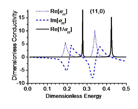
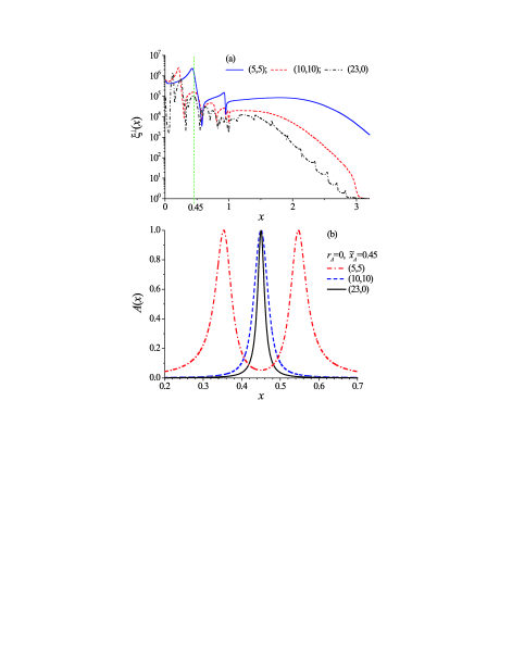
Figure 3 (a) shows the functions for the atom in the center of the (5,5), (10,10) and (23,0) CNs (calculated as described in Refs. Bondarev02 ; Bondarev04 ; Bondarev04pla ; Bondarev05 ; Bondarev04ssc ; Bondarev06trends ). They are seen to decrease with increasing the CN radius, representing the decrease of the atom-field coupling strength as the atom moves away from the CN wall. To calculate the normalized absorption curves in this case, the atomic transition frequency was fixed at [vertical dashed line in Fig. 3 (a)] since this is the approximate peak position of for all the three CNs. Figure 3 (b) shows the result. For the (5,5) CN, the absorption line is split into two components, indicating the strong atom-field coupling with the Rabi splitting corresponding to the energy of eV. The splitting is disappearing with increasing the CN radius, and the absorption line shape becomes Lorentzian with the narrower widths for the larger radii CNs.
3. Atomic States Entanglement in CNs
Two identical two-level atoms (pair of atomic qubits), and , located at and close to a CN, are coupled to the common medium-assisted vacuum-type electromagnetic field via their transition dipole moments. Both atomic dipole moments are, as before, assumed to be directed along the CN axis, . Also assumed is that the atoms are located far enough from each other, to simplify the problem by ignoring the interatomic Coulomb interaction. The total secondly quantized Hamiltonian of the system of the two identical atoms and the nanotube is then written as follows Bondarev07 [compare with Eq. (1)]
| (9) | |||
The Pauli operators, , and with , describe the atomic subsystem and electric dipole transitions between its two states, upper with either of the two atoms in its upper state and lower with both atoms in their lower states, separated by the transition frequency . The renormalized transition frequencies are the same for both of the atoms.
For single-quantum excitations, the time-dependent wave function of the whole system can be written as
| (10) | |||
where , and are the probability amplitudes for the upper states and the lower state of the system, respectively. For the following it is convenient to introduce the new variables
that are the expansion coefficients of the wave function (10) in terms of the maximally entangled two-qubit atomic states . In view of Eqs. (9) and (10), the time-dependent Schrödinger equation yields then (dimensionless variables — Section 2)
| (11) |
where
| (12) | |||
| (13) | |||
| (14) |
The functions are only unequal to zero when the two atoms are initially in their ground states, with the initial excitation residing in the nanotube. Equation (14) assumes that this is realized by selecting the time origin to be right after the time interval , that is necessary for the (excited) atom to decay completely into the nanotube photonic modes, has elapsed. The two-particle local photonic DOS functions
are the generalizations of the DOS functions of Section 2 (see Refs. Bondarev04 ; Bondarev05 ; Bondarev06trends ; Bondarev07 for more details).
The entanglement of the two quantum bits occurs when the two-qubit wave function cannot be represented as a product of the two one-qubit states in any basis. To determine this quantity, a recipe based on the ”spin flip” transformation (see Ref. Wooters for details) and valid for an arbitrary number of the qubits is used. First, the reduced density matrix is defined
that describes the bipartite atomic subsystem in terms of the wave function (10) of the whole system. Next, the ”concurrence”
is introduced, where with being the Pauli matrix that represents the ”spin flip” transformation in the atom single-qubit space. This, after some algebra, becomes
| (15) |
with given by the integral equation (11). Finally, the degree of the entanglement of the two-qubit atomic state (”entanglement of formation” Wooters ) is given by
| (16) |
where .
The entanglement is maximal when the coefficients and are maximally different from each other. For this to occur, the functions in Eqs. (11)–(14) should be different in their values. These are determined by whose frequency behavior is determined by the CN surface axial conductivity (Fig. 2). The functions are computed as described in Ref. Bondarev07 . Then, the integral equation (11) is solved numerically to obtain , followed by the ”concurence” (15) and the entanglement of formation (16).
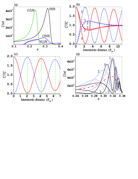
Shown in Fig. 4 (a) is a typical frequency behavior of the one-particle transverse photonic DOS in the infrared and visible frequency range for the atom inside ’zigzag’ CNs of increasing radii. The DOS resonances are seen to be much sharper for metallic CNs () than for semiconducting ones () in agreement with the fact that this frequency range is dominated by the classical Drude-type conductivity which is larger in metallic CNs Bondarev02 . Figure 4 (b) shows the normalized two-particle local photonic DOS functions taken at the resonance frequencies of the respective ’s [Fig. 4 (a)], as functions of the distance between the two atoms on the axes of the (10,0), (11,0) and (12,0) CNs. The values of and are seen to be substantially different from each other before they reach their limit values of at sufficiently large interatomic separations. For metallic CNs the functions and exhibit resonator-like behavior, i.e. they vary periodically in antiphase almost without damping with increasing interatomic separation. In Fig. 4 (c) is shown the dependence of [peak position of in Fig. 4 (a)] on the interatomic separation for the atoms in the center of the metallic (9,0) CN. As the separation increases, and may differ greatly one from another in a periodic way. The maximal difference is , making the mixing coefficients different and thus resulting in a substantial degree of the entanglement of the two spatially separated atomic qubits.
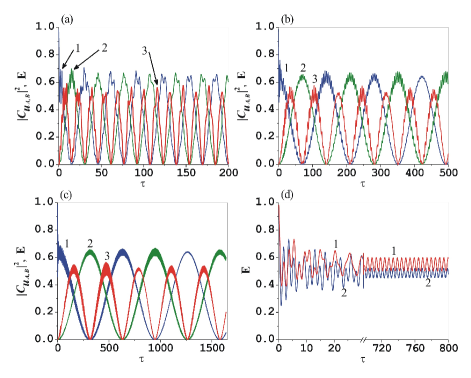
The ensuing spontaneous decay dynamics and atomic entanglement are presented in Fig. 5 (a),(b),(c) for the atoms separated by the three different distances [shown by the vertical dashed lines in Fig. 4 (c)] in the center of the (9,0) CN. Atom is assumed to be initially excited while atom is in its ground state. The entanglement is seen to reach the amount of 0.5 and to vary with time periodically without damping at least for the (reasonably long) times we restricted ourselves in our computations. As the interatomic separation increases, so the period of the entanglement oscillations does while no change occurs in the maximal entanglement. Figure 5 (d) shows the short-time and long-time entanglement evolution when both of the atoms are initially maximally entangled [ while ] and separated by the distance of Å. The entanglement is slightly larger in the case where and no damping occurs as before. Note that the atoms can be separated by longer distances with roughly the same entanglement due to the periodicity with interatomic distance.
4. Exciton-Surface-Plasmon Coupling in Pristine Semiconducting CNs
The total Hamiltonian of an exciton interacting with vacuum-type electromagnetic fluctuations (no external electromagnetic field is assumed to be applied) on the surface of a pristine single-walled semiconducting carbon nanotube is of the form Bondarev08
| (17) |
where the three terms represent the free field, the free exciton, and their interaction, respectively. Here, the second quantized electromagnetic field Hamiltonian is
| (18) |
with the scalar bosonic field operators and creating and annihilating, respectively, the (vacuum-type) medium-assisted surface electromagnetic excitation of frequency at an arbitrary point associated with a carbon atom (representing a lattice site) on the surface of the CN of radius . The summation is made over all the carbon atoms, and may be replaced by the integration over the entire nanotube surface according to the rule
where is the area of an elementary equilateral triangle selected around each carbon atom in a way to cover the entire surface of the nanotube, with Å being the carbon-carbon interatomic distance.
The second quantized Hamiltonian of the free exciton (see, e.g., Ref. Haken ) is of the following form
| (19) |
where the operators and create and annihilate, respectively, an exciton with energy at the lattice site of the CN surface. The index refers to the internal degrees of freedom of the exciton. Alternatively, creates ( is the number of the lattice sites) and annihilates the -internal-state exciton with the quasi-momentum , where is quantized due to the transverse confinement effect and is continuous. The exciton total energy is given by
| (20) |
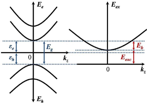
with the first term representing the excitation energy, , of the -internal-state exciton with the (negative) binding energy , created via the interband transition with the band gap , where are transversely quantized azimuthal electron-hole subbands (see the schematic in Fig. 6). The second term represents the kinetic energy of the translational longitudinal movement of the exciton with the effective mass , where and are the electron and hole effective masses, respectively. The two equivalent free-exciton Hamiltonian representations are related to one another via the obvious orthogonality relationships and with the -summation running over the first Brillouin zone of the nanotube. The bosonic field operators in Eq. (18) are transformed to the -representation in the same way.
The most general (non-relativistic, electric dipole) exciton-electromagnetic-field interaction on the nanotube surface can be written in the form Bondarev08 ; Bondarev05 ; Bondarev06trends
| (21) |
where is the total electron momentum operator at the lattice site under the optical dipole transition resulting in the exciton formation at the same site, is the corresponding transition dipole moment operator [related to via the equation ], and are the speed of light and the electron charge, respectively. The vector potential operator (the Coulomb gauge is assumed) and the scalar potential operator represent, respectively, the nanotube’s transversely polarized surface electromagnetic modes and longitudinally polarized surface electromagnetic modes which the exciton interacts with,
with the total electric field operator given by
and representing the -component of the transverse (longitudinal) Green tensor of the electromagnetic subsystem (the nanotube). This Green tensor is different from that used for atomically doped CNs in Sections 2 and 3 above since now there is no additional atomic source in the problem. The Green tensor is derived by expanding the solution of the Green equation in cylindrical coordinates and determining the Wronskian normalization constant from the appropriately chosen boundary conditions on the CN surface Jackson ; Bondarev04 ; Bondarev06trends .
Equations (17)–(21) form the complete set of equations describing the exciton-photon coupled system on the CN surface in terms of the electromagnetic field Green tensor and the CN surface axial conductivity.
It is important to realize that the transversely polarized surface electromagnetic mode contribution to the interaction Hamiltonian from Eq. (21) (first term) is negligible compared to the longitudinally polarized surface electromagnetic mode contribution (second term). The point is that, because of the nanotube quasi-one-dimensionality, the exciton quasi-momentum vector and all the relevant vectorial matrix elements of the momentum and dipole moment operators are directed predominantly along the CN axis (the longitudinal exciton). This prevents the exciton from the electric dipole coupling to transversely polarized surface electromagnetic modes as they propagate predominantly along the CN axis with their electric vectors orthogonal to the propagation direction. The longitudinally polarized surface electromagnetic modes are generated by the electronic Coulomb potential (see, e.g., Ref. Landau ), and therefore represent the CN surface plasmon excitations. These have their electric vectors directed along the propagation direction. They do couple to the longitudinal excitons on the CN surface. Such modes were observed in Ref. Pichler98 . They occur in CNs both at high energies (well-known -plasmon at eV) and at comparatively low energies of eV. The latter ones are related to transversely quantized interband (inter-van Hove) electronic transitions. These weakly-dispersive modes Pichler98 ; Kempa02 are similar to the intersubband plasmons in quantum wells Kempa89 . They occur in the same energy range of eV where the exciton excitation energies are located in small-diameter ( nm) semiconducting CNs Spataru05 ; Ma .
The Hamiltonian (17)–(21) can be diagonalized exactly using Bogoliubov’s canonical transformation technique (see, e.g., Ref. Davydov ), to yield Bondarev08
| (22) |
where the new operator
annihilates and creates the coupled exciton-plasmon excitation of branch , and are the (appropriately chosen) canonical transformation coefficients, . The ”vacuum” energy represents the state with no exciton-plasmons excited in the system, and is the exciton-plasmon energy given by the solution of the following (dimensionless) dispersion relation Bondarev08 ; Bondarev09
| (23) |
Here,
the function
represents the (dimensionless) exciton spontaneous decay rate, where is the longitudinal exciton transition dipole moment matrix element, and the function
| (24) |
stands for the surface plasmon DOS responsible for the exciton decay rate variation due to its coupling to the surface plasmon modes. In Eq. (24), is the fine-structure constant and is the dimensionless CN surface axial conductivity per unit length.
Note that the conductivity factor in Eq. (24) equals
in view of the equation
representing the Drude relation for CNs, where is the longitudinal dielectric function, and are the surface area of the tubule and the number of tubules per unit volume, respectively Bondarev04 ; Bondarev05 ; Bondarev06trends ; Tasaki . This relates very closely the surface plasmon DOS function (24) to the loss function measured in Electron Energy Loss Spectroscopy (EELS) experiments to determine the properties of collective electronic excitations in solids Pichler98 .
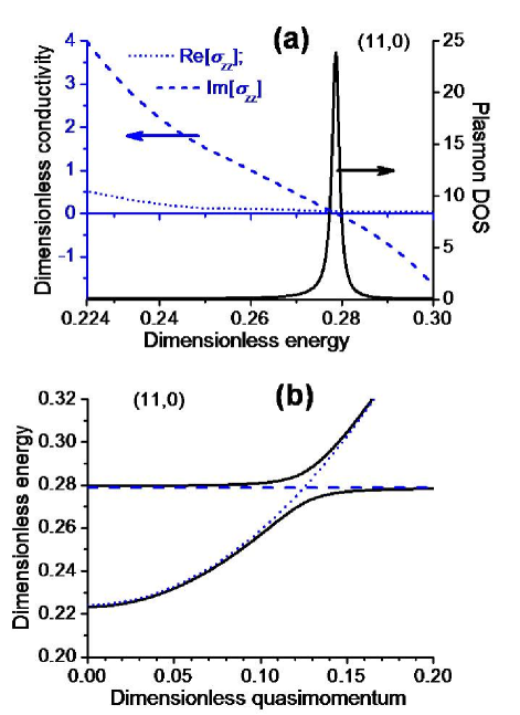
Figure 2 above shows the low-energy behavior of the functions and for the (11,0) nanotube taken as an example ( nm). The function is only non-zero when the two conditions, and , are fulfilled simultaneously Kempa02 ; Kempa89 ; LinShung97 . These result in the peak structure of and of the surface plasmon DOS function (24), respectively. The plasmon DOS peaks represent the surface plasmon modes associated with the transversely quantized interband electronic transitions in CNs Kempa02 (transitions in between the azimuthal electron-hole subbands in the left panel of Fig. 6).
Figure 7 (a) shows the lowest-energy plasmon DOS resonance of the (11,0) CN Bondarev09 as given by Eq. (24). The corresponding fragments of the nanotube’s real and imaginary conductivities are also shown there for comparison. The lower dimensionless energy limit is set up to be equal to the lowest bright exciton excitation energy [ eV () for the (11,0) CN as reported in Ref.Spataru05 by directly solving the Bethe-Salpeter equation]. The peak of the DOS function is seen to exactly coincide in energy with the zero of {or the zero of }, clearly indicating the plasmonic nature of the CN surface excitations under consideration Kempa02 ; Kempa . Also seen in Fig. 7 that the interband plasmon excitations occur in CNs slightly above the first bright exciton excitation energy Ando . This is a unique feature of the complex dielectric response function — the consequence of the general Kramers-Krönig relation VogelWelsch .
The sharp peak structure of the surface plasmon DOS may be used to solve the dispersion equation (23) analytically. Using the Lorentzian approximation
with and being, respectively, the position and the half-width-at-half-maximum of the plasmon resonance closest to the lowest bright exciton excitation energy, the integral in Eq. (23) simplifies to the form
where . This is valid for all in Eq. (23) apart from those located in the narrow interval in the vicinity of the plasmon resonance, provided that the resonance is sharp enough. Then, the dispersion equation becomes the biquadratic equation for with the following two positive solutions of interest (the dispersion curves)
| (25) |
Here, (the -function is expanded into series to linear terms in ).
The two dispersion curves of Eq. (25) are shown in Fig. 7 (b) for the (11,0) nanotube Bondarev09 as functions of the dimensionless longitudinal quasi-momentum. In these calculations, the dipole interband transition matrix element in was estimated from the equation (according to Hanamura’s general theory of the exciton radiative decay in spatially confined systems Hanamura ), where is the exciton intrinsic radiative lifetime, and with being the exciton total energy given by Eq. (20). For zigzag-type nanotubes, the first Brillouin zone of the longitudinal quasi-momentum is given by Dresselhaus ; Dai . The total energy of the ground-internal-state exciton can then be written as with representing the dimensionless longitudinal quasi-momentum. The lowest bright exciton parameters eV, ps, and ( is the free-electron mass) were used for the (11,0) CN as reported in Ref.Spataru05 from the numerical solution of the Bethe-Salpeter equation.
The dispersion curves in Fig. 7 (b) demonstrate a clear anticrossing behavior with the (Rabi) energy splitting eV. This indicates the formation of the strongly coupled surface plasmon-exciton excitations. Note that here the strong exciton-plasmon interaction is supported by an individual quasi-1D nanostructure, a single-walled (small-diameter) semiconducting carbon nanotube, as opposed to the artificially fabricated metal-semiconductor nanostructures studied previously Bellessa ; Govorov ; Fedutik where the metallic component normally carries the plasmon and the semiconducting one carries the exciton. It is also important that the effect comes not only from the height but also from the width of the plasmon resonance as is seen from the definition of the factor in Eq. (25). In other words, as long as the plasmon resonance is sharp enough (which is always the case for interband plasmons), the effect is determined by the area under the plasmon peak in the DOS function (24) rather then by the peak height as one would expect.
The theory of Section 2 can be applied to obtain the optical absorption lineshape (optical response) for the surface exciton-plasmons in CNs. A slight difference now is that the exciton-phonon scattering should also be taken into account as a concurrent process to scatter the exciton in addition to the exciton-plasmon scattering. In the relaxation time approximation for the exciton-phonon scattering, the (dimensionless) exciton absorption lineshape function in the vicinity of the plasmon resonance is then of the form Bondarev09
| (26) |
with
and being the exciton energy broadening due to the exciton-phonon scattering with the relaxation time .
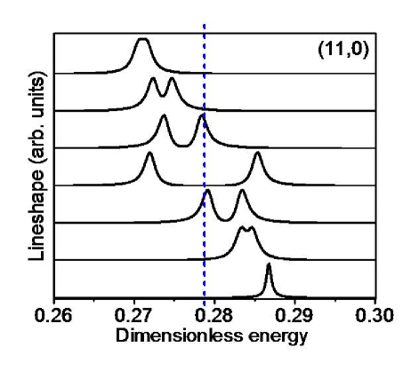
Figure 8 shows the calculated exciton absorption lineshapes as the exciton energy is tuned to the nearest plasmon resonance of the (11,0) CN. In these calculations, the phonon relaxation time fs was used as reported in Ref. Perebeinos05 . The line (Rabi) splitting effect is seen to be eV, indicating the strong exciton-plasmon coupling with the formation of the mixed surface plasmon-exciton excitations. The splitting is not masked by the exciton-phonon scattering, and is expected to be larger in smaller diameter nanotubes.
Obviously, the formation of the strongly coupled mixed exciton-plasmon states is only possible if the exciton total energy is in resonance with the energy of an interband surface plasmon mode. The exciton energy might be tuned to the nearest plasmon resonance in ways used for the excitons in semiconductor quantum microcavities — thermally (by elevating sample temperature) Reithmaier ; Yoshie ; Peter , and/or electrostatically MillerPRL ; Miller ; Zrenner ; Krenner (via the quantum confined Stark effect with an external electrostatic field applied perpendicular to the CN axis). The two possibilities influence the different degrees of freedom of the quasi-1D exciton — the (longitudinal) kinetic energy and the excitation energy, respectively [see Eq. (20)]. In the latter case, in spite of the fact that the cylindrical surface symmetry of the excitonic states brings new peculiarities, the general qualitative behavior of the quantum confined Stark effect in CNs should be similar to what was previously observed and theoretically analyzed for semiconductor quantum wells MillerPRL ; Miller . One should expect that the exciton excitation energy and the interband plasmon energy both shift to the red due to the decrease in the CN band gap as the perpendicular electrostatic field increases. However, the exciton red shift is expected to be much less due to the decrease in the absolute value of the exciton (negative) binding energy Bondarev09aps , which is estimated to be in small-diameter carbon nanotubes Pedersen03 ; Pedersen04 ; Wang05 ; Capaz and thus contributes largely to the exciton excitation energy. So, the exciton excitation energy and the interband plasmon energy will be approaching as the field increases, bringing the total exciton energy [see Eq. (20)] in resonance with the plasmon mode due to the non-zero longitudinal kinetic energy term at finite temperature.
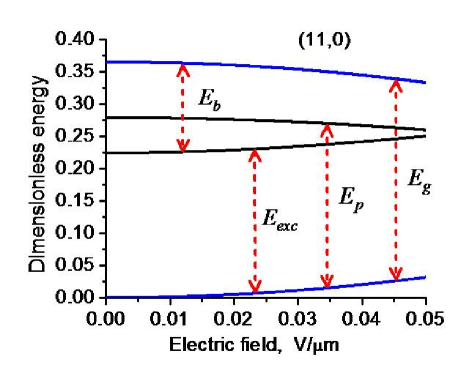
Figure 9 shows the results of the recent calculations of the quantum confined Stark effect for the (11,0) nanotube Bondarev09aps , which confirm the qualitative expectations just discussed. More details on these calculations and the complete theory of the quantum confined Stark effect in CNs will be published elsewhere.
5. Conclusion
Similar to semiconductor microcavities and photonic band-gap materials, carbon nanotubes may qualitatively change the character of the atom-electromagnetic-field interaction, yielding the strong atom-field coupling. For atoms (ions) doped into small-diameter ( nm) nanotubes, the effect of the optical absorption line splitting (Rabi splitting) of eV is predicted in the vicinity of the energy of the atomic transition. This is at least three orders of magnitude larger than the Rabi splitting of eV observed recently in the photoluminescence experiments for exciton-polaritons in quantum dots in semiconductor microcavities Reithmaier ; Yoshie ; Peter . The larger effect in atomically doped CNs comes from the facts that (i) typical atomic binding energies are at least three orders of magnitude larger than typical excitonic binding energies in solids, and (ii) the effective mode volume of the medium-assisted vacuum-type electromagnetic field in the CNs is small enough to achieve Rabi splitting of eV in 1 nm-diameter nanotubes.
Rear-earth Eu3+ complexes in hydrocarbon solvents might be good candidates to test this prediction. They are known to be excellent probes to study quantum optics phenomena in spatially confined systems such as dielectric microspheres Schniepp , or photonic crystals Gaponenko , owing to the dominant narrow, easily detectible dipole transition between two deep-lying electronic levels of europium that essentially create a two-level system.
Metallic carbon nanotubes of nm diameter are demonstrated theoretically to be very efficient, even at room temperatures, to entangle a pair of the spatially separated atomic qubits located in the middle of the nanotube, provided they interact with the same resonance of nanotube’s local photonic DOS. This latter condition is automatically satisfied for identical atoms doped into the nanotube. The entanglement greatly exceeds 0.35 (known to be the maximal value one can achieve in the weak atom-field coupling regime Dung ), and persists with no damping for very long times. Such a behavior is attributed to the strong atom-field coupling and electronic structure resulting in the resonator-like distance dependence of the two-particle local photonic DOS in metallic CNs. Thus, similar to quasi-0D excitonic polaritons in quantum dots in semiconductor microcavities suggested recently to be a possible way to produce the excitonic qubit entanglement Hughes , small-diameter metallic atomically doped carbon nanotubes might represent a novel approach towards solid-state quantum information transfer over long distances — centimeter-long distances, as a matter of fact, since centimeter-long small-diameter single-walled CNs are currently technologically available Zheng ; Huang .
In the current version of the theory outlined here, all the possible decoherence mechanisms in the two-qubit system coupled to nanotube’s surface electromagnetic mode are taken into account in terms of the relaxation time approximation in the CN surface conductivity. The conductivity appears in the photonic DOS and plays a crucial role in the entanglement of formation. It is also important that the method of entanglement preparation described here does not involve the spin degrees of freedom — just a normal, but strong, electric dipole coupling to the same local (single-particle) photonic DOS resonance of the nanotube is required to entangle the pair of spatially separated atomic qubits, as opposed to the spin entanglement studied recently in other fullerene-based models Benjamin . The outlined entanglement scheme can be further generalized to the multi-atom entanglement via the nearest neighbor pairwise quantum correlations, thus challenging novel applications of atomically doped CNs in quantum information science.
In pristine small-diameter ( nm) semiconducting CNs, the strong exciton-surface-plasmon coupling effect is demonstrated with the characteristic exciton absorption line (Rabi) splitting eV. This is almost as large as the typical exciton binding energies in such CNs ( eV Pedersen03 ; Pedersen04 ; Wang05 ; Capaz ), and of the same order of magnitude as the exciton-plasmon Rabi splitting in organic semiconductors ( meV Bellessa ). Also, this is much larger than the exciton-polariton Rabi splitting in semiconductor microcavities (Reithmaier ; Yoshie ; Peter ), or the exciton-plasmon Rabi splitting in hybrid semiconductor-metal nanoparticle molecules Govorov . Also important is that the strong exciton-plasmon coupling effect takes place in an individual carbon nanotube as opposed to artificially fabricated hybrid plasmonic nanostructures just mentioned. To bring the exciton in resonance with nanotube’s nearest plasmon mode, the exciton energy can be tuned in ways used for the excitons in semiconductor quantum microcavities — thermally (by elevating sample temperature) Reithmaier ; Yoshie ; Peter , and/or electrostatically MillerPRL ; Miller ; Zrenner ; Krenner (via the quantum confined Stark effect with an external electrostatic field applied perpendicular to the CN axis). The two possibilities affect the different degrees of freedom of the quasi-1D excitons in CNs — the (longitudinal) kinetic energy and the excitation energy, respectively.
To conclude, the surface electromagnetic field phenomena reviewed here have a great potential to open up new paths for the development of the CN based tunable optoelectronic device applications in areas such as nanophotonics, nanoplasmonics, cavity quantum electrodynamics, and quantum information science.
I Acknowledgements
This work was supported by the US National Science Foundation (grants ECS-0631347 and HRD-0833184), the US Department of Defense (grant W911NF-05-1-0502) and NASA (grant NAG3-804). Discussions with M.A.Braun, J.Finley, S.V.Gaponenko, M.F.Gelin, A.O.Govorov, A.Kleinhammes, J.Liu, G.E.Malashkevich, H.Qasmi, B.Vlahovic, L.Woods, and Y.Wu are gratefully acknowledged.
References
- (1) R.Saito, G.Dresselhaus, and M.S.Dresselhaus, Science of Fullerens and Carbon Nanotubes (Imperial College Press, London, 1998).
- (2) H.Dai, Surf. Sci. 500 (2002) 218.
- (3) L.X.Zheng, M.J.O’Connell, S.K.Doorn, X.Z.Liao, Y.H. Zhao, E.A.Akhadov, M.A.Hoffbauer, B.J.Roop, Q.X.Jia, R.C.Dye, D.E.Peterson, S.M.Huang, J.Liu and Y.T.Zhu, Nature Materials 3 (2004) 673.
- (4) S.M.Huang, B.Maynor, X.Y.Cai, and J.Liu, Advanced Materials 15 (2003) 1651.
- (5) R.H.Baughman, A.A.Zakhidov, and W.A.de Heer, Science 297 (2002) 787.
- (6) A.Popescu, L.M.Woods, and I.V.Bondarev, Nanotechnology 19 (2008) 435702.
- (7) J.E.Trancik, S.C.Barton, and J.Hone, Nanoletters 8 (2008) 982.
- (8) S.Latil, F.Triozon, and S.Roche, Phys. Rev. Lett. 95 (2005) 126802.
- (9) Y.-W.Son, J.Ihm, M.L.Cohen, S.G.Louie, and H.J.Choi, Phys. Rev. Lett. 95 (2005) 216602.
- (10) L.Duclaux, Carbon 40 (2002) 1751.
- (11) H.Shimoda, B.Gao, X.P.Tang, A.Kleinhammes, L.Fleming, Y.Wu, and O.Zhou, Phys. Rev. Lett. 88 (2002) 015502.
- (12) G.-H. Jeong, A.A.Farajian, R.Hatakeyama, T.Hirata, T.Yaguchi, K.Tohji, H.Mizuseki, and Y.Kawazoe, Phys. Rev. B 68 (2003) 075410.
- (13) G.-H.Jeong, A.A.Farajian, T.Hirata, R.Hatakeyama, K. Tohji, T.M.Briere, H.Mizuseki, and Y.Kawazoe, Thin Solid Films 435 (2003) 307.
- (14) M.Khazaei, A.A.Farajian, G.-H.Jeong, H.Mizuseki, T. Hirata, R.Hatakeyama, and Y.Kawazoe, J. Phys. Chem. B 108 (2004) 15529.
- (15) M.M.Calbi, M.W.Cole, S.M.Gatica, M.J.Bojan, and G.Stan, Rev. Mod. Phys. 73 (2001) 857.
- (16) I.V.Bondarev and B.Vlahovic, Phys. Rev. B 74 (2006) 073401.
- (17) I.V.Bondarev and B.Vlahovic, Phys. Rev. B 75 (2007) 033402.
- (18) I.V.Bondarev, J. Electron. Mater. 36 (2007) 1579.
- (19) I.V.Bondarev, Optics & Spectroscopy (Springer) 103 (2007) 366.
- (20) T.Pedersen, Phys. Rev. B 67 (2003) 073401.
- (21) T.Pedersen, Carbon 42 (2004) 1007.
- (22) R.B.Capaz, C.D.Spataru, S.Ismail-Beigi, and S.G.Louie, Phys. Rev. B 74 (2006) 121401(R).
- (23) C.D.Spataru, S.Ismail-Beigi, L.X.Benedict, and S.G. Louie, Phys. Rev. Lett. 92 (2004) 077402.
- (24) F.Wang, G.Dukovic, L.E.Brus, and T.F.Heinz, Phys. Rev. Lett. 92 (2004) 177401.
- (25) F.Wang, G.Dukovic, L.E.Brus, and T.F.Heinz, Science 308 (2005) 838.
- (26) A.Hagen, M.Steiner, M.B.Raschke, C.Lienau, T.Hertel, H.Qian, A.J.Meixner, and A.Hartschuh, Phys. Rev. Lett. 95 (2005) 197401.
- (27) F.Plentz, H.B.Ribeiro, A.Jorio, M.S.Strano, M.A.Pimenta, Phys. Rev. Lett. 95 (2005) 247401.
- (28) F.Xia, M.Steiner, Y.-M.Lin, and Ph.Avouris, Nature Nanotechnology 6 (2008) 609.
- (29) A.Högele, Ch.Galland, M.Winger, and A.Imamolu, Phys. Rev. Lett. 100 (2008) 217401.
- (30) B.F.Habenicht and O.V.Prezhdo, Phys. Rev. Lett. 100 (2008) 197402.
- (31) V.Perebeinos, J.Tersoff, and Ph.Avouris, Phys. Rev. Lett. 94 (2005) 027402.
- (32) M.Lazzeri, S.Piscanec, F.Mauri, A.C.Ferrari, and J.Robertson, Phys. Rev. Lett. 95 (2005) 236802.
- (33) S.Piscanec, M.Lazzeri, J.Robertson, A.Ferrari, and F. Mauri, Phys. Rev. B 75 (2007) 035427.
- (34) I.V.Bondarev and H.Qasmi, Physica E 40 (2008) 2365.
- (35) I.V.Bondarev, K.Tatur, and L.M.Woods, Opt. Commun. 282 (2009) 661.
- (36) S.Zaric, G.N.Ostojic, J.Shaver, J.Kono, O.Portugall, P.H.Frings, G.L.J.A.Rikken, M.Furis, S.A.Crooker, X. Wei, V.C.Moore, R.H.Hauge, and R.E.Smalley, Phys. Rev. Lett. 96 (2006) 016406.
- (37) A.Srivastava, H.Htoon, V.I.Klimov, and J.Kono, Phys. Rev. Lett. 101 (2008) 087402.
- (38) V.Perebeinos and Ph.Avouris, Nano Lett. 7 (2007) 609.
- (39) M.S.Dresselhaus, G.Dresselhaus, R.Saito, and A.Jorio, Annu. Rev. Phys. Chem. 58 (2007) 719.
- (40) T.Brandes, Phys. Rep. 408 (2005) 315.
- (41) A.S.Srensen, C.H. van der Wal, L.I.Childress, and M.D.Lukin, Phys. Rev. Lett. 92 (2004) 063601.
- (42) S.C.Benjamin, A.Ardavan, G.A.D.Briggs, D.A.Britz, D.Gunlycke, J.Jefferson, M.A.G. Jones, D.F.Leigh, B.W.Lovett, A.N.Khlobystov, S.A.Lyon, J.J.L.Morton, K.Porfyrakis, M.R.Sambrook. and A.M.Tyryshkin, J. Phys.: Condens. Matter 18 (2006) S867.
- (43) S.Hughes, Phys. Rev. Lett. 94 (2005) 227402.
- (44) J.I.Cirac, P.Zoller, H.J.Kimble, and H.Mabuchi, Phys. Rev. Lett. 78 (1997) 3221.
- (45) I.V.Bondarev, G.Ya.Slepyan and S.A.Maksimenko, Phys. Rev. Lett. 89 (2002) 115504.
- (46) I.V.Bondarev and Ph.Lambin, Phys. Rev. B 70 (2004) 035407.
- (47) I.V.Bondarev and Ph.Lambin, Phys. Lett. A 328 (2004) 235.
- (48) I.V.Bondarev and Ph.Lambin, Phys. Rev. B 72 (2005) 035451.
- (49) I.V.Bondarev and Ph.Lambin, Solid State Commun. 132 (2004) 203.
- (50) I.V.Bondarev and Ph.Lambin, in: Trends in Nanotubes Reasearch (Nova Science, NY, 2006). Ch.6, pp.139-183.
- (51) L.C.Andreani, G.Panzarini, and J.-M.Gérard, Phys. Rev. B 60 (1999) 13276.
- (52) A.S.Davydov, Quantum Mechanics (Pergamon, New York, 1976).
- (53) J.P.Reithmaier, G.Sȩk, A.Löffler, C.Hofmann, S.Kuhn, S.Reitzenstein, L.V.Keldysh, V.D.Kulakovskii, T.L.Reinecke, and A.Forchel, Nature 432 (2004) 197.
- (54) T.Yoshie, A.Scherer, J.Hendrickson, G.Khitrova, H.M. Gibbs, G.Rupper, C.Ell, O.B.Shchekin, and D.G.Deppe, Nature 432 (2004) 200.
- (55) E.Peter, P.Senellart, D.Martrou, A.Lemaître, J.Hours, J.M.Gérard, and J.Bloch, Phys. Rev. Lett. 95 (2005) 067401.
- (56) T.Pichler, M.Knupfer, M.S.Golden, J.Fink, A.Rinzler, and R.E.Smalley, Phys. Rev. Lett. 80 (1998) 4729.
- (57) C.D.Spataru, S.Ismail-Beigi, R.B.Capaz, and S.G.Louie, Phys. Rev. Lett. 95 (2005) 247402.
- (58) Y.-Z.Ma, C.D.Spataru, L.Valkunas, S.G.Louie, and G.R. Fleming, Phys. Rev. B 74 (2006) 085402.
- (59) J.Bellessa, C.Bonnand, J.C.Plenet, and J.Mugnier, Phys. Rev. Lett. 93 (2004) 036404.
- (60) W.Zhang, A.O.Govorov, and G.W.Bryant, Phys. Rev. Lett. 97 (2006) 146804.
- (61) Y.Fedutik, V.V.Temnov, O.Schöps, U.Woggon, and M.V. Artemyev, Phys. Rev. Lett. 99 (2007) 136802.
- (62) W.Vogel and D.-G.Welsch, Quantum Optics (Wiley-VCH, NY, 2006). Ch.10, p.337.
- (63) L.Knöll, S.Scheel, and D.-G.Welsch, in: Coherence and Statistics of Photons and Atoms, edited by J.Peřina (Wiley, NY, 2001).
- (64) S.Y.Buhmann and D.-G.Welsch, Prog. Quantum Electron. 31 (2007) 51.
- (65) H.T.Dung, S.Scheel, D.-G.Welsch, and L.Knoll, J. Opt. B: Quant. & Semiclass. Optics 4 (2002) S169.
- (66) L.X.Benedict, S.G.Louie, and M.L.Cohen, Phys. Rev. B 52 (1995) 8541.
- (67) S.Tasaki, K.Maekawa, and T.Yamabe, Phys. Rev. B 57 (1998) 9301.
- (68) Z.M.Li, Z.K.Tang, H.J.Liu, N.Wang, C.T.Chan, R.Saito, S.Okada, G.D.Li, J.S.Chen, N.Nagasawa, and S.Tsuda, Phys. Rev. Lett. 87 (2001) 127401.
- (69) A.G.Marinopoulos, L.Reining, A.Rubio, and N.Vast, Phys. Rev. Lett. 91 (2003) 046402.
- (70) T.Ando, J. Phys. Soc. Jpn. 74 (2005) 777.
- (71) B.Kozinsky and N.Marzari, Phys. Rev. Lett. 96 (2006) 166801.
- (72) W.Heitler, The quantum Theory of Radiation (Clarendon, Oxford, 1954).
- (73) M.F.Lin, D.S.Chuu, and K.W.-K.Shung, Phys. Rev. B 56 (1997) 1430.
- (74) H.Ehrenreich and M.H.Cohen, Phys. Rev. 115 (1959) 786.
- (75) V.N.Popov, L.Henrard, Phys. Rev. B 70 (2004) 115407.
- (76) W.K.Wooters, Phys. Rev. Lett. 80, 2245 (1998).
- (77) H.Haken, Quantum Field Theory of Solids, (North-Holland, Amsterdam, 1976).
- (78) J.D.Jackson, Classical Electrodynamics (Wiley, New York, 1975).
- (79) L.D.Landau and E.M.Lifshits, The Classical Theory of Fields (Pergamon, New York, 1975).
- (80) K.Kempa and P.R.Chura, special edition of the Kluwer Academic Press Journal, edited by L.Liz-Marzan and M.Giersig (2002).
- (81) K.Kempa, D.Broido, C.Beckwith, and J.Cen, Phys. Rev. B 40 (1989) 8385.
- (82) K.Kempa, Phys. Rev. B 66 (2002) 195406.
- (83) E.Hanamura, Phys. Rev. B 38 (1988) 1228.
- (84) H.Schniepp and V.Sandoghdar, Phys. Rev. Lett. 89 (2002) 257403.
- (85) S.V.Gaponenko, V.N.Bogomolov, E.P.Petrov, A.M.Kapitonov, D.A.Yarotsky, I.I.Kalosha, A.A.Eychmueller, A.L.Rogach, J.McGilp, U.Woggon, and F.Gindele, J. Lightwave Technology 17 (1999) 2128.
- (86) D.A.B.Miller, D.S.Chemla, T.C.Damen, A.C.Gossard, W.Wiegmann, T.H.Wood, and C.A.Burrus, Phys. Rev. Lett. 53 (1984) 2173.
- (87) D.A.B.Miller, D.S.Chemla, T.C.Damen, A.C.Gossard, W.Wiegmann, T.H.Wood, and C.A.Burrus, Phys. Rev. B 32 (1985) 1043.
- (88) A.Zrenner, E.Beham, S.Stufler, F.Findeis, M.Bichler, and G.Abstreiter, Nature 418 (2002) 612.
- (89) H.J.Krenner, E.C.Clark, T.Nakaoka, M.Bichler, C.Scheurer, G.Abstreiter, and J.J.Finley, Phys. Rev. Lett. 97 (2006) 076403.
- (90) I.V.Bondarev and J.McConnell, In: Bulletin of the American Physical Society, Vol. 54, No 1, Q11.00002.