Two-dimensional electron liquid state at LaAlO3-SrTiO3 interfaces
Abstract
Using tunneling spectroscopy we have measured the spectral density of states of the mobile, two-dimensional electron system generated at the LaAlO3-SrTiO3 interface. As shown by the density of states the interface electron system differs qualitatively, first, from the electron systems of the materials defining the interface and, second, from the two-dimensional electron gases formed at interfaces between conventional semiconductors.
pacs:
73.20.-r, 73.40.Gk, 71.15.MbTwo-dimensional (2D) conducting electron systems are generated at interfaces between a large variety of insulating oxides Ohtomo and Hwang (2004); Mannhart et al. (2008). These interfaces show a broad spectrum of different properties. The quantum-Hall effect has been found Tsukazaki et al. (2007), for example, for the electron system at the ZnO-(MgxZn1-xO) interface. For the interface between LaTiO3 and SrTiO3, first explored experimentally by Ohtomo and Hwang Ohtomo et al. (2002), spin ordering and ferro-orbital ordering has been predicted Okamoto et al. (2006). The most widely investigated electron system at oxide interfaces is the metallic state created at the interface between the charge transfer insulators LaAlO3 and TiO2-terminated SrTiO3 Ohtomo and Hwang (2004). This electron system forms a 2D superconductor with a of mK that is easily tunable by electric gate fields Caviglia et al. (2008). The LaAlO3-SrTiO3 interface has also been predicted Pentcheva and Pickett (2006) and reported Brinkman et al. (2007) to develop magnetic order.
While several theoretical models have been developed to describe the electronic properties of these interfaces Pavlenko and Kopp (unpublished); Pentcheva and Pickett (2009); Schwingenschlögl and Schuster (2009a, b), less information on the electronic structure has been provided by experiments. At room temperature its thickness has been inferred from scanning tunneling microscopy (STM) writing experiments Cen et al. (2008), from photoemission Sing et al. (2009), and from cross-sectional STM (Ref. Basletic et al., 2008) to be at most a few nanometers. Further, hard x-ray photoelectron emission has shown that the charge carriers at the interface occupy Ti states Sing et al. (2009). Studies of x-ray absorption spectroscopy furthermore revealed that energetically the crystal-field split Ti levels are rearranged, such that the levels are the first available states for the conducting electrons Salluzzo et al. (2009).
The spectral density of states (DOS) at the interface is a fundamental property that characterizes the electron system. As it furthermore can be calculated as well as measured, it is a key property for the understanding of the electron system at the interface. For measurements of the spectral DOS scanning tunneling spectroscopy (STS) is a powerful technique Feenstra (1994), which has been used extensively to characterize 2D electron gases (2DEGs) in semiconductor systems. STS was employed, in particular, to probe surfaces of semiconducting thin films where electrons are confined by the film thickness Perraud et al. (2008). STS was also used successfully to analyze cross-sectional cleavage planes of semiconductor heterostructures Salemink et al. (1989); Suzuki et al. (2007). In addition, semiconductor surfaces, below which electrons are confined in band bending regions induced by ion implantation Wolovelsky et al. (1998) or surfaces at which electron gases were generated by adsorbates Morgenstern et al. (2003), were explored.
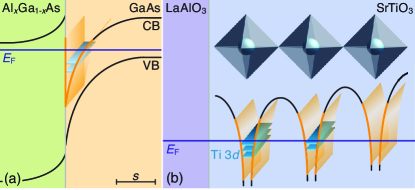
Here we report on STS measurements of the spectral DOS of the electron system at the LaAlO3-SrTiO3 interface. We find the measured DOS to be in excellent agreement with the interface DOS calculated in density-functional theory (DFT), providing evidence that the tunneling current in the STS measurements is carried by interface states. The measured spectrum of the interface DOS and therefore the electron system differs qualitatively from the DOS of doped bulk SrTiO3 or LaAlO3. The electron system cannot be accurately described as a thin layer of doped SrTiO3. The measurements reveal furthermore that the electron system also differs qualitatively from the hitherto known 2D electron systems at interfaces between conventional semiconductors. We find the electrons confined in multiple layers of quantum wells given by the ionic potentials of the TiO6 octahedra. In these wells the electrons are subject to the correlations characteristic of the orbitals of the Ti ions. The spectral DOS is not a step function as is the case for standard semiconductor interfaces but rather resembles the DOS of Ti states. Quantum wells and electronic systems of this kind are unknown from the 2DEGs in conventional semiconductors, in graphene or in ZnO.
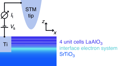
For the studies, we fabricated LaAlO3-SrTiO3 heterostructures with 4 unit-cell (uc) thick ( nm) epitaxial LaAlO3 layers to obtain measurable tunneling currents. This thickness was chosen because it is the minimum thickness required to generate the conducting interface Thiel et al. (2006). For larger LaAlO3 thicknesses the tunneling current densities become impractically small. The samples were grown by standard pulsed laser deposition as described in Ref. epa, . For deposition the SrTiO3 substrates were heated to 780C in an oxygen background pressure of mbar. The LaAlO3 film growth was monitored by reflection high-energy electron diffraction. While SrTiO3 surfaces are known to show numerous surface reconstructions Herger et al. (2007); Lu et al. (2010); Deak et al. (2007); Eglitis and Vanderbilt (2008); Wang et al. (2009); Silly et al. (2006); Kubo and Nozoye (2003); Newell et al. (2007), x-ray diffraction showed no evidence of distortions of the LaAlO3 films, which could be attributed to a SrTiO3 surface reconstruction, suggesting that the LaAlO3 growth stabilizes the standard SrTiO3 structure at the interface. Titanium plugs filling ion etched holes were used to contact the interfaces. After a heating procedure in a preparation chamber epa , the samples were transferred in situ to the scanning probe microscope (SPM), which operates in ultrahigh vacuum at K. An iridium spall attached to a cantilever based on a quartz tuning fork Giessibl (1998) with a spring constant of 1800 Nm was used as a tip. The tip was treated in situ by field emission epa . The cantilever was not excited mechanically during STM and STS measurements. The experimental setup is sketched in Fig. 1. Typical measurement parameters were tunneling currents of 10 pA, sweep rates of Vs and scanning speeds of 10 nms.

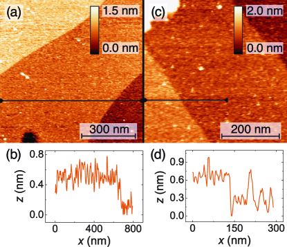
Imaging the LaAlO3-SrTiO3 heterostructures by frequency modulation scanning force microscopy Albrecht et al. (1991) (FM-SFM) as well as by constant current STM revealed the standard step-and-terrace structure resulting from the slight miscut of the SrTiO3 substrates (Fig. 2). While on more conventional samples excellent resolution was achieved with the SPM employed Hembacher et al. (2004), it was impossible to obtain atomic resolution on the LaAlO3-SrTiO3 heterostructures epa .

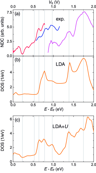
Conductance-voltage characteristics were measured using a standard lock-in technique epa . Simultaneously, the tunneling current was measured as a function of voltage. The normalized differential conductance was determined as a measure of the sample DOS Feenstra et al. (1987). The spectra were taken on sample areas where the step-and-terrace structure was resolved in STM topography. We found the characteristic spectroscopic features to be reproducible across four samples epa . Figure 3(a) shows a representative dependence of the NDC on voltage. The conductances are minute for negative voltages (tunneling from occupied sample states). For positive voltages (tunneling into unoccupied sample states) the spectroscopically accessible energy range is limited at low voltages by small tunneling conductances and at high voltages by large electric fields destabilizing the tunneling gap. To measure the tunneling characteristics at a given sample location over a large voltage range, several spectra were therefore taken at different tip-sample separations as determined according to the tunneling currents at given gap voltages . Three characteristics measured with different tip-sample separations, from two different samples, are shown in Fig. 3(a). In these spectra, clear peaks are seen at , , , , and V.

To identify the electron states carrying the measured tunneling current and to explore the role of electronic correlations at the interface we compare the measured DOS to predictions of DFT. We performed local-density approximation (LDA) and LDA calculations Blaha et al. (2001); Anisimov et al. (1993) of the layer-resolved DOS of LaAlO3-SrTiO3 heterostructures. Further information on these calculations is given in Ref. epa, . While differences are present in details, the calculated state densities and the effective electron mass of bare electron masses are consistent with those reported in Refs. Schwingenschlögl and Schuster, 2008; Pentcheva and Pickett, 2009; Pavlenko and Kopp, unpublished, and Copie et al., 2009.
In Fig. 3(b) the Ti DOS of the interface TiO2 layer calculated using LDA for a supercell with a 4 uc thick LaAlO3 layer on SrTiO3 is shown. According to the calculation, electronic reconstruction leads to a doping of O states located in the topmost AlO2 layer with holes and of Ti states located at the interface with electrons. Experimentally, it is only the interface which is found to be conducting. In the total DOS between 0 and 2 eV the Ti orbitals located in the interfacial TiO2 layer prevail. The other, small, contributions are provided by the TiO2 planes of adjacent SrTiO3 layers and, below eV, by the O states of the surface. The Ti states contribute at energies above eV and the La states at energies above eV. The measured peaks at , , and V are also present in the calculated DOS. The measured peaks at and V, however, are not represented in the LDA result.
The LDA calculations of the interface electron system consider an on-site Coulomb repulsion eV and a Hund coupling eV in the Ti shell. The choice of conservative values for and does not imply these values characterize the system best. Figure 3(c) shows the DOS calculated for the supercell using LDA. The DOS exhibits additional peaks at and eV, generated by the splitting of the Ti bands due to the interorbital interactions caused by the finite and . Remarkably, these peaks are observed experimentally but are missing in the LDA DOS.
We note that the experimental hump at eV is broader than the corresponding structure in LDA. However, LDA generates a structure of approximately the measured width but with finer structures. These fine structures reflect the formation of the upper Hubbard bands, which is a fundamental effect of correlated electron systems, arising when is on the order of the bandwidth or larger. Indeed, the calculated width of the Ti band is eV.
The good agreement between experiment and calculation suggests that the electron states carrying the measured tunneling current are the ones calculated in DFT. For energies between and 2 eV, mainly Ti and Ti orbitals of the interface TiO2 layer contribute to the calculated DOS and the prominent peaks result from these orbitals; tunneling occurs into Ti orbitals at the interface, the significant contributions arising from the Ti states. These results are consistent with the results of recent photoabsorption measurements Salluzzo et al. (2009), from which it was concluded that the lowest unoccupied states are Ti 3 states.

The fact that the experimental DOS is matched significantly better by the LDA calculation than by the LDA calculation provides evidence that the electron system at the interface is correlated with substantial values of and on the Ti orbitals. Therefore, this 2D electron system is a liquid. This electron liquid is formed by correlated electrons, which can move parallel to the interface, but are constrained in their perpendicular motion by the Coulomb potentials of the titanium ions of the final TiO2 layers and also, to a smaller degree, by band bending (Fig. 4).
Interfaces in oxides therefore broaden the spectrum of available 2D electron systems from the 2DEGs of conventional semiconductors to also include systems with sizable electronic correlations. Such correlation effects, in combination with the already intriguing physics of 2D electron systems, promise unprecedented electronic phenomena. Influenced by electronic correlations generated in the ionic lattices of the oxides, electron systems at oxide interfaces have exceptional properties, possibly enabling devices with hitherto unknown characteristics.
We thank D. Bonn, R. Claessen, M. Fiebig, F. J. Giessibl, J. Repp, C. W. Schneider and D. Vollhardt for helpful discussions. This work was supported by the Deutsche Forschungsgemeinschaft (TRR 80) and by the European Union (OxIDes). J. R. Kirtley was supported by the Alexander von Humboldt foundation. Grants of computer time from the Leibniz-Rechenzentrum München through HLRB (h1181) and DEISA (OXSIM) are gratefully acknowledged.
References
- Ohtomo and Hwang (2004) A. Ohtomo and H. Y. Hwang, Nature (London) 427, 423 (2004).
- Mannhart et al. (2008) J. Mannhart et al., MRS Bull. 33, 1027 (2008).
- Tsukazaki et al. (2007) A. Tsukazaki et al., Science 315, 1388 (2007).
- Ohtomo et al. (2002) A. Ohtomo et al., Nature (London) 419, 378 (2002).
- Okamoto et al. (2006) S. Okamoto et al., Phys. Rev. Lett. 97, 056802 (2006).
- Caviglia et al. (2008) A. D. Caviglia et al., Nature (London) 456, 624 (2008).
- Pentcheva and Pickett (2006) R. Pentcheva and W. E. Pickett, Phys. Rev. B 74, 035112 (2006).
- Brinkman et al. (2007) A. Brinkman et al., Nature Mater. 6, 493 (2007).
- Pavlenko and Kopp (unpublished) N. Pavlenko and T. Kopp, arXiv:0901.4610 (unpublished).
- Pentcheva and Pickett (2009) R. Pentcheva and W. E. Pickett, Phys. Rev. Lett. 102, 107602 (2009).
- Schwingenschlögl and Schuster (2009a) U. Schwingenschlögl and C. Schuster, Chem. Phys. Lett. 467, 354 (2009a).
- Schwingenschlögl and Schuster (2009b) U. Schwingenschlögl and C. Schuster, EPL 86, 27005 (2009b).
- Cen et al. (2008) C. Cen et al., Nature Mater. 7, 298 (2008).
- Sing et al. (2009) M. Sing et al., Phys. Rev. Lett. 102, 176805 (2009).
- Basletic et al. (2008) M. Basletic et al., Nature Mater. 7, 621 (2008).
- Salluzzo et al. (2009) M. Salluzzo et al., Phys. Rev. Lett. 102, 166804 (2009).
- Feenstra (1994) R. M. Feenstra, Surf. Sci. 299-300, 965 (1994).
- Perraud et al. (2008) S. Perraud et al., Phys. Rev. Lett. 100, 056806 (2008).
- Salemink et al. (1989) H. W. M. Salemink et al., Appl. Phys. Lett. 54, 1112 (1989).
- Suzuki et al. (2007) K. Suzuki et al., Phys. Rev. Lett. 98, 136802 (2007).
- Wolovelsky et al. (1998) M. Wolovelsky et al., Phys. Rev. B 57, 6274 (1998).
- Morgenstern et al. (2003) M. Morgenstern et al., Phys. Rev. Lett. 90, 056804 (2003).
- Thiel et al. (2006) S. Thiel et al., Science 313, 1942 (2006).
- (24) See supplementary material for more data and details on sample preparation, STM tip treatment, experimental parameters, the STS lock-in technique, and the DFT calculations.
- Herger et al. (2007) R. Herger et al., Phys. Rev. Lett. 98, 076102 (2007).
- Lu et al. (2010) C. Lu et al., J. Phys. Chem. C 114, 3416 (2010).
- Deak et al. (2007) D. S. Deak et al., Nanotechnology 18, 075301 (2007).
- Eglitis and Vanderbilt (2008) R. I. Eglitis and D. Vanderbilt, Phys. Rev. B 77, 195408 (2008).
- Wang et al. (2009) Z. Wang et al., Appl. Phys. Lett. 95, 021912 (2009).
- Silly et al. (2006) F. Silly et al., Surf. Sci. 600, 219 (2006).
- Kubo and Nozoye (2003) T. Kubo and H. Nozoye, Surf. Sci. 542, 177 (2003).
- Newell et al. (2007) D. T. Newell et al., Phys. Rev. B 75, 205429 (2007).
- Giessibl (1998) F. J. Giessibl, Appl. Phys. Lett. 73, 3956 (1998).
- Albrecht et al. (1991) T. R. Albrecht et al., J. Appl. Phys. 69, 668 (1991).
- Hembacher et al. (2004) S. Hembacher et al., Science 305, 380 (2004).
- Feenstra et al. (1987) R. M. Feenstra et al., Surf. Sci. 181, 295 (1987).
- Blaha et al. (2001) P. Blaha, K. Schwarz, G. K. H. Madsen, D. Kvasnicka, and J. Luitz, WIEN2k (K. Schwarz, Vienna University of Technology, Vienna, Austria, 2001).
- Anisimov et al. (1993) V. I. Anisimov et al., Phys. Rev. B 48, 16929 (1993).
- Schwingenschlögl and Schuster (2008) U. Schwingenschlögl and C. Schuster, EPL 81, 17007 (2008).
- Copie et al. (2009) O. Copie et al., Phys. Rev. Lett. 102, 216804 (2009).