Electrical Detection and Magnetic-Field Control of Spin States in Phosphorus-Doped Silicon
Abstract
Electron paramagnetic resonance of ensembles of phosphorus donors in silicon has been detected electrically with externally applied magnetic fields lower than 200 G. Because the spin Hamiltonian was dominated by the contact hyperfine term rather than by the Zeeman terms at such low magnetic fields, superposition states and were formed between phosphorus electron and nuclear spins, and electron paramagnetic resonance transitions between these superposition states and or states are observed clearly. A continuous change of and with the magnetic field was observed with a behavior fully consistent with theory of phosphorus donors in silicon.
pacs:
76.90.+d, 72.20.Jv, 71.55.-i, 76.30.-vI Introduction
A phosphorus in silicon is attracting much attention towards realization of solid-state quantum information processors. It can be viewed as a two-qubit system having one 31P nuclear spin () and one electron spin (). Kane ; Kane2000 ; all-silicon ; Sarovar ; EDMRQC Coherent manipulation of its electronic states, MarNP ; MarPRL ; GWMPRL08 ; FelarXiv coherent transfer of states between electron and nuclear-spins, entofPinSi and large hyperpolarization of nuclear spins BoehmePRL2009 ; YSSPRL2009 have been demonstrated recently. Thanks to phosphorus’s long spin dephasing time, Tyryshkin ; Abe enrichment of silicon with nuclear spin-free 28Si has suppressed the background isotope fluctuation significantly SiIsotope1 ; SiIsotope2 to make possible the optical detection of 31P nuclear spin states. PLE Because a standard electron paramagnetic resonance (EPR) measurement requires at least 109 spins or more, much more sensitive electrical detection methods of phosphorus EPR have been attracting attention. MarNP ; MarPRL ; GWMPRL08 ; FelarXiv ; MMSPRL2008 ; Solomon ; Stich:JAP77 ; Stich:d-a ; Stich:APL68 ; pointdefect ; P50 ; HighEDMR ; Honig57 The record so far reported is the detection of 50 phosphorus spin states P50 and extensive efforts are underway worldwide to detect single phosphorus spin states. YMM09 All of the previous phosphorus EPR studies have been performed in the “high-magnetic-field regime,” which can be defined as 200 G for phosphorus in silicon as we demonstrate later, and have observed two EPR allowed transitions. MarNP ; MarPRL ; GWMPRL08 ; FelarXiv ; BoehmePRL2009 ; Solomon ; P50 ; HighEDMR ; Honig57 The present work reports electrically detected magnetic resonance (EDMR) of phosphorus spin states in silicon which shows five of six possible transitions expected for the phosphorus donors in silicon under the low magnetic field 200 G.
The spin Hamiltonian of an isolated phosphorus atom placed in an externally applied magnetic field is given by;
| (1) |
where and are electron and phosphorus nuclear spins, respectively. The first, second, and third terms represent the electron Zeeman, nuclear Zeeman, and contact hyperfine interaction between phosphorus electron and nuclear spins, respectively. Here GHz/T and MHz/T are given by electron and nuclear -factors and , respectively. CE ; NuclMom The hyperfine constant is MHz. Feher1959 Eigenstates of this spin Hamiltonian are given by;
| (2) | |||||
| (3) | |||||
| (4) | |||||
| (5) |
where and . is the angle between externally applied magnetic field direction and actual electron and nuclear spins precession axis given by . P-pESR A magnetic quantum number is represented by () and an arrow on the left (right) in each ket represents the electron (nuclear) spin state. Fig. 1(a) shows the magnetic field dependence of the four states expected for phosphorus in silicon. At the high magnetic fields ( G) and , i.e., the four states simply become , , , and . The EPR allowed transitions in this regime are limited to two: and . In the low-magnetic-field regime defined by 200 G, the eigenstates of and change continuously because , i.e., and , change significantly with as shown in Fig. 1(b). Therefore, the degree of superposition between and that determines the EPR allowed transitions also changes with . For example, the transition at the high magnetic field corresponds to the nuclear magnetic resonance (NMR) and it cannot be observed as the EPR. However, the same transition becomes EPR observable at the low magnetic field because the EPR allowed component emerges with . Note that transitions and are weak because they are allowed only in the second order. Nevertheless, two aspects of quantum control that cannot be realized in the high-magnetic-field regime is expected to become possible in the low-magnetic-field regime; 1) controlling the ratio of and to change the degree of superposition by the magnetic field and 2) changing the population of the four states by utilizing the six transitions that are made allowed. The present work demonstrates these properties experimentally using electrical detection of phosphorus EPR and develops a quantitative theoretical model to support our observation.

II Experimental
A sample was a bulk Czochralski-grown n-type silicon single crystal having phosphorus concentration 1016 cm-3. It was cut into a rectangular shape of the dimension 821 mm3. Ohmic contacts were prepared at both ends of the long axis by arsenic implantation of at 25 keV followed by annealing at 980 ∘C for 25 seconds and vacuum deposition of the 5-nm-thick palladium and 50-nm-thick gold layers. The sample was placed in a cryostat with optical windows. A white light from a halogen lamp placed outside of the cryostat was focused onto the sample through the optical window for steady state excitation of the electron-hole pairs to maintain the sample resistance at 10 k. The sample was connected with a series resistor of 10 k. A constant voltage of typically 10 V was applied to the series of the sample and resistor. A coaxial cable was used to connect a RF source with an irradiation coil whose opposite side was connected to a 50 terminator. Externally applied magnetic field was provided by a 300 mm bore electrical magnet. Another pair coil was placed in the cryostat to modulate the externally applied magnetic field for the lock-in detection of the divider voltage corresponding to the change in the sample photoconductivity (EDMR signal).
III Results and Discussions
III.1 EDMR peak positions
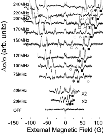
Fig. 2 shows the EDMR signals obtained at = 5 K. By changing the irradiation frequencies, six different transition peaks labeled , , , , , and are observed clearly.

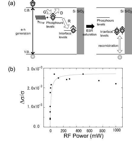
Fig. 3 shows externally applied magnetic field vs. RF frequencies of the six observed resonance positions. Solid curves are theoretically expected results for different transitions of phosphorus in silicon using Eqs. (2) - (5) that are calculated rigorously with no fitting parameter. The excellent quantitative agreement between our experiment and theory supports the successful observation of the transitions listed in the captions of Figs. 1, 2, and 3.
The transition indicated by agrees very well with the theoretically predicted resonance positions for labeled by . However, we conclude that this peak is composed predominantly by the EPR transition of the paramagnetic defects situating around the interface between bulk Si and native surface oxide SiO2 for the following reasons. As apparent from Fig. 1(a), the transition indicated by corresponds to a typical electron Zeeman transition whose energy is approximately proportional to . Therefore, EPR transition energies of other defects with very little hyperfine interaction, such as those of the interface spin states, Lepine ; Pb overlap with this transition. Here the EPR of the interface spin state is allowed in the first order and, therefore, expected to have strong intensity. However, the transition labeled by is allowed only in the second order and should demonstrate approximately the same intensity as the transition labeled by in Fig. 2. The fact that the intensity of being much stronger than that of suggests that the transition arises predominantly from the EPR transition of the interface defects that is allowed in the first order. The importance of the presence of the interface defects was confirmed by removing the surface oxide using a dilute hydrofluoric (HF) solution. The HF treatment made all of the EDMR signals nearly invisible. Leaving the sample for a few days in air to cover the sample surface with native oxide again retrieved the intensity of the all EDMR signals completely.
III.2 RF power and magnetic field dependencies of the phosphorus EDMR
The fact that the presence of the surface oxide is needed to observe the EDMR signals allows us to develop a theoretical model describing the RF power and magnetic field dependencies of the EDMR signal intensity as the following. We assume that the interface defects act as spin-dependent recombination centers for electrons bound to phosphorus donors. In this sense, our model is an extension of existing two-level spin-dependent recombination model MarNP ; MarPRL ; GWMPRL08 ; FelarXiv ; Stich:JAP77 ; Stich:d-a ; pointdefect ; White77 ; KSM ; Haberkorn80 ; L'vov82 ; Vlasenko95 ; compKSM ; Barabanov98 ; exchangeofEDMR to the four levels. The spin Hamiltonian of the system during EDMR is given by
| (6) |
Here the nuclear Zeeman term is neglected because is approximately times smaller than and the coupling term ( where and are the electron spins of the phosphorus and interface states, respectively) is also neglected assuming . The second term arises from the RF irradiation and this perturbation term is defined as to calculate the transition probability for the system described by Eq. (6) using the Fermi’s golden rule,
| (7) |
The electron-hole recombination via interface states takes place only when and form a spin singlet and does not occur when they form a spin triplet to establish a “spin blockade.” Ono
| Phosphorus | Interface | Recombination rate | |
|---|---|---|---|
| 0 | |||
| + | |||
| + | |||
| + | |||
| + | |||
| 0 |
Other important essences of our model are described in the caption of Fig. 4(a). Let us consider where or is one of the four phosphorus spin states as defined by Eqs. (2) - (5) and where or corresponds to spin up or down of the interface state, respectively. Using , , and defined in Fig. 4(a), we obtain the rate equation
| (8) |
where is the total number of electron pairs and is the number of electron pairs in spin states and . The recombination rates that have been obtained using the method described in Ref. 43 are listed in Table 1. The pairs with () with correspond to the spin blockade. Now we consider a representing example where the irradiated RF is in resonance with the transition. In this case;
| (9) | |||
| (10) |
where is the transition probability that is proportional to the RF irradiation power around the origin. ex3 This partly lifts the spin blockade and promotes the recombination. The steady state solution for the number of electron recombining becomes;
| (11) | |||
| (12) |
Then the EDMR signal intensity is obtained as;
| (13) |
This result shows that the signal intensity is proportional to the irradiated RF power and, therefore, to around the origin. This corresponds to our experimental observation shown in Fig. 4(b) when is defined as . A solid curve shown in the figure is the successful fitting by Eqs. (12) and (13) using , , , and as fitting parameters D A set of appropriate values we found are = 6.4 cm-3, = 5.0 sec-1, = 2.3 sec-1, and = 1.7 sec-1.
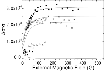
Finally, we show in Fig. 5 the magnetic field dependence of the EDMR signal intensity. We used the RF power of 500 mW, which was large enough to saturate the signal as shown in Fig. 4(b). Here . Now the two ’s in Eq. (12) are replaced by a constant;
| (14) |
Such relations with appropriate have been used to fit representative experimental results shown in Fig. 5. Note that our model is not applicable to second-order allowed transitions such as and . From the fitting of the first-order allowed transition, we obtain a set of appropriate values = 1.0 cm-3, = 6.7 sec-1, = 2.9 sec-1, and = 7.0 sec-1. Note that the magnetic field dependence of and employed here is same as the one shown in Fig. 1(b). Therefore, the excellent agreement between our experiment and model shows that the coefficients of superposition can be controlled by the choice of and reach the maximally entangled states in the limit of = 0 as expected. Bennett96
Similarly, we can derive a relation for the interface center EDMR, since the rotation of the interface electron spin also lifts the spin blockade and enhances the recombination. We consider again a rate equation using , , , and to obtain the same as Eq. (13) but different from the phosphorus resonance case: ex2
| (15) |
When the signal intensity is saturated, is given by;
| (16) |
This result has been used to fit the behavior of the interface center peak () in Fig. 5. A set of appropriate values we found are = 8 cm-3, = 2.0 sec-1, = 3.6 sec-1, and = 3.9 sec-1. Here the values of , , and are approximately the same as the ones obtained for phosphorus but the value of is different.
A significance of the results shown in Fig. 5 is that the intensity of transitions changes below 200 G in accordance with theory. The standard EPR allows for observation of only and because in the high magnetic fields. However, the value of increases with decreasing the magnetic field, especially for the magnetic fields below 200 G, and approaches 1/ as 0. Naturally, the intensity of and decreases because the components of the EPR allowed and diminish. For the same reason transitions such as and appear only when 200 G. This observation leads us to conclude that it is possible to form the superposition states between electron and nuclear spins of phosphorus in the regime of the low magnetic field 200 G. Their superposition coefficients and can be controlled simply by selecting an appropriate magnetic field.
IV Conclusion
Electron paramagnetic resonance spectroscopy of an ensemble of phosphorus donors in silicon has been performed successfully to map out the behavior of phosphorus spin states at the magnetic field lower than 200 G. Formation of the superposition states and has been confirmed with the values of and changing continuously with the magnetic field in accordance with theory of phosphorus in silicon. Dependencies of the EDMR signal intensity on the RF power and magnetic field have been described successfully by a model assuming a spin-dependent recombination of phosphorus electrons via defects situating around the oxide/silicon interface.
V Acknowledgment
We thank Martin Brandt for fruitful discussion. This work was supported in part by a Grant-in-Aid for Scientific Research by MEXT Specially Promoted Research 18001002, in part by Special Coordination Funds for Promoting Science and Technology, in part by the JST-DFG Strategic Cooperative Program on Nanoelectronics, in part by the Strategic Information and Communications R&D Promotion Program (SCOPE) from the Ministry of Internal Affairs and Communications of Japan and in part by a Grant-in-Aid for the Global Center of Excellence at Keio University.
References
- (1) B. E. Kane, Nature 393, 133 (1998).
- (2) B. E. Kane, Fort. Physik 48, 1023 (2000).
- (3) K. M. Itoh, Solid State Commun. 133, 747 (2005).
- (4) M. Sarovar, K. C. Young, T. Schenkel, and K. B. Whaley, Phys. Rev. B 78, 245302 (2008).
- (5) C. Boehme and K. Lips, Phys. Stat. Sol. (b) 233, 427 (2002).
- (6) A. R. Stegner, C. Boehme, H. Huebl, M. Stutzmann, K. Lips, and M. S. Brandt, Nature Phys. 2, 835 (2006).
- (7) H. Huebl, F. Hoehne, B. Grolik, A. R. Stegner, M. Stutzmann, and M. S. Brandt, Phys. Rev. Lett. 100, 177602 (2008).
- (8) G. W. Morley, D. R. McCamey, H. A. Seipel, L.-C. Brunel, J. van Tol, and C. Boehme, Phys. Rev. Lett. 101, 207602 (2008).
- (9) F. Hoehne, H. Huebl, B. Galler, M. Stutzmann, and M. S. Brandt, arXiv:0908.3612 (2009).
- (10) J. J. L. Morton, A. M. Tyryshkin, R. M. Brown, S. Shankar, B. W. Lovett, A. Ardavan, T. Schenkel, E. E. Haller, J. W. Ager, and S. A. Lyon, Nature 455, 1085 (2008).
- (11) D. R. McCamey, J. van Tol, G. W. Morley, and C. Boehme, Phys. Rev. Lett. 102, 027601 (2009).
- (12) A. Yang, M. Steger, T. Sekiguchi, M. L. W. Thewalt, T. D. Ladd, K. M. Itoh, H. Riemann, N. V. Abrosimov, P. Becker, and H.-J. Pohl, Phys. Rev. Lett. 102, 257401 (2009).
- (13) A. M. Tyryshkin, J. J. L. Morton, S. C. Benjamin, A. Ardavan, G. A. D. Briggs, J. W. Ager, and S. A. Lyon, J. Phys. Comd. Matt. 18, S783 (2006).
- (14) E. Abe, K. M. Itoh, J. Isoya, and S. Yamasaki, Phys. Rev. B 70, 033204 (2004).
- (15) K. M. Itoh, J. Kato, F. Uemura, A. K. Kaliteyevskii, O. N. Godisov, G. G. Devyatych, A. D. Bulanov, A. V. Gusev, I. D. Kovalev, P. G. Sennikov, H.-J. Pohl, N. V. Abrosimov, and H. Riemann, Jpn. J. Appl. Phys. 42, 6248 (2003).
- (16) K.Takyu, K. M. Itoh, K. Oka, N. Saito, and V. I. Ozhogin, Jpn. J. Appl. Phys. 38, L1493 (1999).
- (17) A. Yang, M. Steger, D. Karaiskaj, M. L. W. Thewalt, M. Cardona, K. M. Itoh, H. Riemann, N. V. Abrosimov, M. F. Churbanov, A. V. Gusev, A. D. Bulanov, A. K. Kaliteevskii, O. N. Godisov, P. Becker, H.-J. Pohl, J. W. Ager III, and E. E. Haller, Phys. Rev. Lett. 97, 227401 (2006).
- (18) G. W. Morley, D. R. McCamey, H. A. Seipel, L.-C. Brunel, J. van Tol, and C. Boehme, Phys. Rev. Lett. 101, 207602 (2008).
- (19) J. Schmidt and I. Solomon, Comptes Rendus de L’Acadmie des Sciences B 263, 169 (1966).
- (20) B. Stich, S. Greulich-Weber, and J.-M. Speath, J. Appl. Phys. 77, 1546 (1995).
- (21) S. Greulich-Weber, B. Stich, and J.-M. Spaeth, Materials Science Forum 196-201, 1509 (1995).
- (22) J.-M. Spaeth and H. Overhof, Point Defects in Semiconductors and Insulators (Springer, 2002), Chap. 7.
- (23) B. Stich, S. Greulich-Weber, and J.-M. Speath, Appl. Phys. Lett. 68, 1102 (1996).
- (24) D. R. McCamey, H. Huebl, M. S. Brandt, W. D. Hutchison, J. C. McCallum, R. G. Clark, and A. R. Hamilton, Appl. Phys. Lett. 89, 182115 (2006).
- (25) D. R. McCamey, G. W. Morley, H. A. Seipel, L.-C. Brunel, J. van Tol, and C. Boehme, Phys. Rev. B 78, 045303 (2008).
- (26) A. Honig and M. Moroz, Rev. Sci. Instrum. 49, 183 (1957).
- (27) K. Y. Tan, K. W. Chan, M. Möttönen, A. Morello, C. Yang, J. van Donkelaar, A. Alves, J. M. Pirkkalainen, D. N. Jamieson, R. G. Clark, and A. S. Dzurak, arXiv:0905.4358v2 (2009).
- (28) C. F. Young, E. H. Poindexter, G. J. Gerardi, W. L. Warren, and D. J. Keeble, Phys. Rev. B 55, 16245 (1997).
- (29) J. E. Mack, Rev. Mod. Phys. 22, 64 (1950).
- (30) G. Feher, Phys. Rev. 114, 1219 (1959).
- (31) A. Schweiger and G. Jeschke, Principles of pulse Electron Paramagnetic Resonance (OXFORD, 2001), Chap. 3, Sec. 3.5, pp.58 - 62.
- (32) D. J. Lpine, Phys. Rev. B 6, 436 (1970).
- (33) J. L. Cantin and H. J. von Bardeleben, J. Non-Cryst. Solids 303, 175 (2002).
- (34) R. M. White and J. F. Gouyet, Phys. Rev. B 16, 2596 (1977).
- (35) D. Kaplam, I. Solomon, and N. F. Mott, Le J. de Phys. Lett. 39, L51 (1978).
- (36) R. Haberkorn and W. Dietz, Solid State Commun. 35, 505 (1980).
- (37) V. S. L’vov, L. S. Mima, and O. V. Tretyak, Sov. Phys. JETP 56, 897 (1982).
- (38) L. S. Vlasenko, Yu. V. Martynov, T. Gregorkiewicz, and C. A. J. Ammerlaan, Phys. Rev. B 52, 1144 (1995).
- (39) A. V. Barabanov, O. V. Tretiak, and V. A. L’vov, Phys. Rev. B 54, 2571 (1996).
- (40) A. V. Barabanov, V. A. Lvov, and O. V. Tretyak, Phys. Stat. Sol. (b) 207, 419 (1998).
- (41) A. Gliesche, C. Michel, V. Rajevac, K. Lips, S. D. Baranovskii, F. Gebhard, and C. Boehme, Phys. Rev. B 77, 245206 (2008).
- (42) A similar phenomenon was observed in transport through double quantum dots in K. Ono et al., Science 297, 1313 (2002).
- (43) is the transition rate of an electron from phosphorus to the interface levels when and form a spin singlet. The transition rate , where is the distance between a phosphorus and an interface state and is the effective Bohr radius of phosphorus (interface) state. It is averaged with the weight of , where is the donor concentration.
- (44) On the other hand, the transition probabilities of , , and are proportional to , and , respectively.
- (45) C. H. Bennett, H. J. Bernstein, S. Popescu, and B. Schumacher, Phys. Rev. A 53, 2046 (1996).
- (46) The rate equations given by , where for and .