Thermoelectric performance of granular semiconductors
Abstract
We study thermoelectric properties of granular semiconductors with weak tunneling conductance between the grains, . We calculate the thermopower and figure of merit taking into account the shift of the chemical potential and the asymmetry of the density of states in the vicinity of the Fermi surface due to n- or p-type doping in the Efros-Shklovskii regime for temperatures less than the charging energy. We show that for weakly coupled semiconducting grains the figure of merit is optimized for grain sizes of order nm for typical materials and its values can be larger than one. We also study the case of compensated granular semiconductors and show that in this case the thermopower can be still finite, although two to three orders of magnitude smaller than in the uncompensated regime.
pacs:
72.20.Pa, 73.63.-b, 73.63.BdA major research area in nano-science and materials physics is the search for highly efficient thermoelectric materials. Although there has been extensive research efforts in the last several decades, the progress in this quest has been limited until recently. It was found that for further improvement in efficiency inhomogeneous/granular thermoelectric semiconductors are especially suited Majumdar . These materials are now accessible as next generation devices for conversion of thermal to electrical energy and vice versa and technologically important due to the possibility of direct control of the system parameters. The dimensionless figure of merit, , is the preferred measure for the performance or efficiency of thermoelectric materials, where is the thermopower and and the electric and thermal conductivities, respectively Rowe ; Mahan . Recently, values of in layered nanoscale structures venka01 at , and for a bulk semiconductors with nanoscale inclusions harman02 at about were reported. These high values of are in the range for applications and therefore call for the development of a comprehensive quantitative description of thermoelectric properties of granular semiconductors, which can serve as basis for a new generation of thermoelectrics.
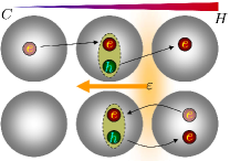
In this paper we investigate the thermopower and the figure of merit of granular semiconductors focusing on the case of weak coupling between the grains, , see Fig. 1. Each semiconducting nanocrystal is characterized by two energy scales: (i) the mean energy level spacing , where is the density of states at the Fermi surface, is the grain size, and is the dimensionality of a grain, and (ii) the charging energy with being the dielectric constant. In semiconductors the density of states is of about two orders of magnitude smaller than that in metals. Thus in semiconducting dots can be of order of the charging energy, , in contrast to metallic granular materials where typically glatz+prb09 . Our considerations are valid for temperatures .
The internal conductance of a grain is taken larger than the inter-grain tunneling conductance, , which controls macroscopic transport properties of the sample Beloborodov07 . In this paper we consider , i.e., smaller than the quantum conductance, which is the typical experimental situation venka01 ; harman02 .

In the case of diagonal (short range) Coulomb interaction, the total probability for an electron tunneling through many grains via elastic or inelastic co-tunneling can be written as the product, , of the individual probabilities of single elastic/inelastic co-tunneling events through single grains with is the number of grains. The probability is related to the localization length as .
Semiconducting nanocrystal arrays are described by the Hamiltonian
| (1) |
where are the grain indexes and the summation in the second term of the r.h.s. of Eq. (1) is performed over nearest neighbors. The term is the Hamiltonian for the single grain including the free electron energy and the diagonal Coulomb interaction, and the second term is the tunneling Hamiltonian between the adjacent grains and with being random tunneling matrix elements and [] the creation [annihilation] operator on the th grain. Due to the large mean energy level spacing in semiconducting grains , only a few terms of the -sums are important.
In Ref. BeloPRB it was shown that the probability for elastic and inelastic co-tunneling through an array of weakly coupled semiconducting grains has the form
| (2) |
where is the electron escape time from a grain. Thus, for the elastic/inelastic localization length we obtain
| (3) |
The localization length is related to the characteristic temperature scale , which is of order .

Below we derive the thermopower, , thermal conductivity, , and figure of merit, for granular semiconductors using Eq. (3).
One remark is in order: The thermopower of lightly doped compensated semiconductors was investigated in the past Fritzsche71 ; Zvyagin73 ; Kosarev74 ; Parfenov07 . However, all previous studies were concentrated on the Mott variable range hopping (VRH) regime, with conductivity being , where is the Mott temperature Mottbook . In granular materials the Mott VRH regime is hard to observe. Indeed, in semiconductors the Efros-Shklovskii (ES) law shklovskii-book ; ES may turn into the Mott behavior with an increase of temperature. This happens when the typical electron energy involved in a hopping process becomes larger than the width of the Coulomb gap , i.e. when it falls into the flat region of the density of states where Mott behavior is expected. To estimate the width of the Coulomb gap , one compares the ES expression for the density of states with the DOS in the absence of the long-range part of the Coulomb interaction, ( is the dimensionality of a sample). Using the condition we obtain . Inserting the value for the bare DOS, , into the last expression we finally obtain . This means that there is no flat region in the DOS for .
Here we discuss two effects: i) we calculate the thermopower of granular semiconductors taking into account the shift of the chemical potential with being the electron filling factor ( is related to the compensation level of semiconductors, here we concentrate on n-type doped semiconductors with ), a dimensionless numerical coefficient, and the asymmetry of the density of states (DOS) with being a numerical constant; ii) we show that even in the absence of the chemical potential shift, , and asymmetry of DOS, , the thermopower is still finite, although small, due to co-tunneling processes. We start with the former case.
To calculate the thermopower of granular materials in the regime of weak coupling between the grains it is necessary to take into account electrons and holes because the contributions of electrons and holes cancel in the leading order. In general the thermopower is proportional to the average energy transferred by charge carriers and can be written as Fritzsche71 ; Zvyagin73 ; Kosarev74 ; Parfenov07
| (4) |
Here the subscripts and refer to electrons and holes and is the shifted chemical potential. The expression in the square brackets of the r.h.s. of Eq. (4) describes the average energy transferred by charge carriers (electron or hole) measured with respect to the shifted chemical potential . The average energy in Eq. (4) can be calculated as follows
| (5) |
Here is the Fermi function for electrons or holes, the typical transfer energy in one hop, and is energy dependent the DOS. As we will see later, it is crucial to take into account the asymmetry of the DOS and the shift of the chemical potential in order to obtain a finite result in Eq. (4).
The DOS, in Eq. (5) for has the following form Zvyagin73
| (6) |
and is constant, , outside the Coulomb gap region, and , where is the width of the Coulomb gap. The shift of the chemical potential and the asymmetry of the DOS, , are explicitly defined above Eq. (4).
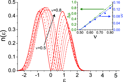
To support our choice for the expression of the DOS in Eq. (6) we numerically compute the DOS for a 2D Coulomb glass model to simulate the whole system of semiconducting grains (see Refs. glatz+prl07 ; glatz+jstat08 for details) at arbitrary filling factor using first principles. The result of the simulations is shown in Fig. 2. These simulations clearly indicate that for a filling factor , the DOS is asymmetric and the chemical potential is shifted. Using these results we can identify the dimensionless numerical coefficients and by a simple linear fit. We note that , thus the contribution to the thermopower caused by in Eq. (7) is dominant.
Now, we can calculate Eq. (5) and the analog contribution for holes using Eq. (6) for the DOS together with the numerically found values for 111We expect that the values for in a 3D Coulomb glass are of the same order as in 2D.. Finally we derive the expression for the thermopower of granular semiconductors in the limit of weak coupling between the grains
| (7) |
We note that the r.h.s. of Eq. (7) vanishes for filling factor , i.e., for compensated semiconductors.
Equation (7) is valid for temperatures and weak coupling between the grains . Under this condition, the electric conductivity is Beloborodov07 ; BeloPRB
| (8) |
The thermal conductivity consists of two parts: the electron, and phonon, . The phonon contribution at temperatures , where is the Debye temperature is given by Ziman ; Mahan00
| (9) |
where is the phonon mean free path in granular semiconductors with being the Fermi length. [For nm, , , one obtains nm at ]

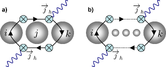
The main contribution to the electric part of the thermal conductivity appears due to a single closed co-tunneling loop (see Fig. 1). An electron executing a co-tunneling loop brings back its charge to the starting grain and hence there is little change in the electrical conductivity and therefore the classical activation term is absent. However, there is no requirement that the returning electron has exactly the same energy (due to inelastic processes). The leading contribution to is proportional to and is depicted in the diagram shown in Fig. 3a). The analytical result corresponding to this process can be estimated as follows
| (10) |
where we used Eq. (2) for the inelastic co-tunneling probability . Since at relatively high temperatures the phonon contribution to thermal conductivity is dominant, we can neglect the contribution in the following.
Substituting Eqs. (7) and (9) into the expression for the figure of merit we obtain the result
| (11) |
Here the expressions for and are given above Eq. (4). Using Eq. (11) we can calculate the temperature at which has its maximum value, given by the solution of the quadratic equation , where . In we get , while in 3D the existence of a maximum depends on the values of and .

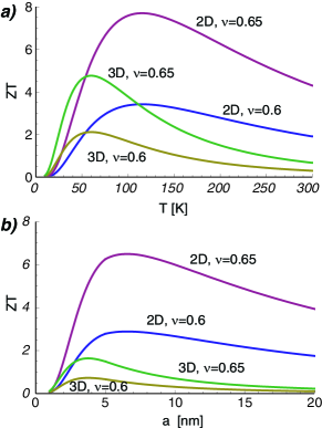
In Fig. 4 we plotted the figure of merit for a two- and three-dimensional system, using typical parameters for granular semiconductors: , , , , and . Figure 4a) shows the temperature dependence of for two different filling factors for a grain size of nm (For this size and the above dielectric constant we get K). We clearly see that the figure of merit can well exceed one. However, we remark that depends inversely proportional on the numerical coefficient of , which is assumed to be one here. Figure 4b) shows the grain size dependence of at fixed temperature K. At this temperature for the above system parameters, the figure of merit is optimal for grain sizes nm in 3D and nm in 2D.
Now, we concentrate on the compensated regime (filling factor ). In this case Eq. (7) predicts zero thermopower . Thus, the fundamental question exists what mechanism may lead to a finite thermopower in this case. We start our consideration with the fact that the thermopower can be expressed in terms of the thermoelectric coefficient and the electric conductivity as . Thus, to calculate the thermopower one has to know the thermoelectric coefficient . To estimate we use the diagram shown in Fig. 3b) (here the tilde indicates the compensated case). Since the dominant contribution to vanishes due to particle-hole symmetry, to obtain a nonzero result it is necessary to take into account the fact that the tunneling matrix elements and the density of states depend on energy. In the leading order, the corrections to both quantities are proportional to , where is Fermi energy glatz+prb09 . As a result, the thermoelecric coefficient is given by the expression
| (12) |
where the temperature scale was defined below Eq. (3). Substituting Eq. (8) and (12) into the expression for thermopower we obtain
| (13) |
It follows that the thermopower is finite although small, leading to a small figure of merit as well, since . Using Eqs. (7) and (13) one can see that the ratio of two thermopowers for compensated [, Eq. (13)] and for n-type (, Eq. (7)) regimes is of order .
In conclusion, we studied thermoelectric properties of granular semiconductors at weak tunneling conductance between the grains, . We calculated the thermopower and figure of merit taking into account the shift of the chemical potential and asymmetry of the density of states for the exemplary case of n-type doping. We showed that the weak coupling between the grains leads to a high thermopower and a low thermal conductivity resulting in relatively high values of the figure of merit. We also discussed the case of compensated (half filling, ) granular semiconductors. We showed that in this regime the thermopower is finite, but rather small.
A. G. was supported by the U.S. Department of Energy Office of Science under the Contract No. DE-AC02-06CH11357.
References
- (1) A. Majumdar, Science 303, 777 (2004).
- (2) D. M. Rowe and C. M. Bhandari, Modern thermoelectrics (Reston, Reston, VA, 1983).
- (3) G. D. Mahan, J. Appl. Phys. 70, 4551 (1991).
- (4) R. Venkatasubramanian, E. Siivola, T. Colpitts, and B O’Quinn, Nature 413, 597 (2001).
- (5) T. C. Harman, P. J. Taylor, M. P. Walsh, B. E. LaForge, Science 297, 2229 (2002).
- (6) A. Glatz and I. S. Beloborodov, Phys. Rev. B 79, 041404 (2009); Phys. Rev. B 79, 235403 (2009).
- (7) I. S. Beloborodov, A. V. Lopatin, V. M. Vinokur, and K. B. Efetov, Rev. Mod. Phys. 79, 469 (2007).
- (8) I. S. Beloborodov, A. Glatz, and V. M. Vinokur, Phys. Rev. B 75, 052302 (2007).
- (9) H. Fritzsche, Solid State Commun. 9, 1813 (1971).
- (10) I. P. Zvyagin, in Hopping Transport in Solids, Ed. by M. Pollak and B. I. Shklovskii (Elsevier, Amsterdam, 1991), p. 143; Phys. Status Solidi B 58, 443 (1973).
- (11) V. V. Kosarev, Fiz. Tekh. Poluprovodn. (Leningrad) 8, 1378 (1974) [Sov. Phys. Semicond. 8, 897 (1974)].
- (12) O. E. Parfenov and F. A. Shklyaruk, Fiz. Tekh. Poluprovodn. 41, 1041 (2007) [Semiconductors 41, 1021 (2007)].
- (13) N. F. Mott, Metal-Insulator Transitions (Taylor and Francis, 1990).
- (14) B. I. Shklovskii and A. L. Efros, Electronic Properties of Doped Semiconductors (Springer, New York, 1984).
- (15) A. L. Efros and B. I. Shklovskii, J. Phys. C 8, L49 (1975).
- (16) A. Glatz, V. M. Vinokur, and Y. M. Galperin, Phys. Rev. Lett. 98, 196401 (2007).
- (17) A. Glatz et al., J. Stat. Mech. 06, P06006 (2008).
- (18) J. Ziman, Electrons and Phonons (Cambridge University Press, 1960).
- (19) M. V. Simkin and G. D. Mahan, cond-mat/0005008.