Aharonov-Bohm Effect at liquid-nitrogen temperature:
Fröhlich superconducting quantum device
Abstract
The Aharonov-Bohm (AB) effect has been accepted and has promoted interdisciplinary scientific activities in modern physics. To observe the AB effect in condensed matter physics, the whole system needs to maintain phase coherence, in a tiny ring of the diameter 1 m and at low temperatures below 1 K. We report that AB oscillations have been measured at high temperature 79 K by use of charge-density wave (CDW) loops in TaS3 ring crystals. CDW condensate maintained macroscopic quantum coherence, which extended over the ring circumference 85 m. The periodicity of the oscillations is in accuracy within a 10 % range. The observation of the CDW AB effect implies Frohlich superconductivity in terms of macroscopic coherence and will provide a novel quantum interference device running at room temperature.
I Introduction
50 years ago, Aharonov and Bohm challenged our understanding of vector potential that had not been a physical entity Aharonov . Since then, the concept of AB (Aharonov and Bohm) phase has been accepted in modern physics Tonomura , such as condensed matter physics Webb ; Altshuler ; AharonovC ; Konig , particle physics Wu , non-abelian gauge theories Horvathy , gravitational physics Ford ; Ashtekar and laser dynamics Hosten . To observe AB phase in condensed matter physics, the whole system needs to maintain phase coherence, in a tiny ring of the diameter 1 m and at low temperatures below 1 K, typically Webb . We report first evidences for the AB interference effect at high temperature 79 K, by use of charge-density wave (CDW) loops in TaS3 ring crystals Tanda whose circumference is as long as 85 m. CDW condensate maintained macroscopic quantum coherence which extended over the ring system Gruner . Periodicity of the AB effect of CDW was half a flux quantum with h and e being Plank constant and an elementary charge, respectively. Using interference of CDWs, a room temperature operating quantum interference device may be produced because some low dimensional materials, such as NbS3, exhibit a CDW transition above room temperature. This will be substituted for superconducting quantum interference devices (SQUIDs), which can be only used at low temperatures.
CDWs have not been considered to exhibit AB effect because an electron-hole pair of CDW has neutral charge that cannot couple to vector potential, and the CDW phase is usually treated as a classical coordinate. However, the first prediction of AB effect of CDW was made by Bogachek et al Bogachek . Their model includes a term representing the interaction of the CDW with the vector potential field, and then estimated the oscillation of . Another theory states that quasi-particle interference is generated by changing the CDW ground state Visscher ; Yi ; Montambaux . Latyshev et al tried to observe the AB effect of CDWs in NbSe3 crystals with tiny random holes pierced by heavy-ion irradiation Latyshev . Oscillation in the nonlinear CDW conductivity as a function of the magnetic field was shown. Visscher et al, however, insisted that this could be the AB effect of a quasi-particle passing through a metallic region where the CDW order was destroyed near the tiny holes Visscher1998 . Therefore, existence of the AB effect of CDW condensate has been an open question as yet.
For this reason, a CDW loop, over which continuity of the CDW order is maintained, should be exploited in order to decide the argument. This cannot be realized simply by piercing a hole in a conventional single crystal, because continuous CDW chain doesn’t be formed with the hole. Topological crystals (ring and Möbius strip shaped seamless crystals) Tanda ; Matsuura are only materials providing such the CDW loop. The chain axis of CDW directs itself along the circumference of the ring without losing the CDW order, thereby forms a CDW loop.
Besides, the previous experiment of NbSe3 had another problem. In the CDW state of NbSe3, there still remain uncondensed electrons, which make it difficult to determine the origin of oscillation. Hence the choice of materials is crucial. We investigated orthorhombic TaS3, which have a Peierls transition at 218 K, and no uncondensed electrons at low temperatures.
II Experimental
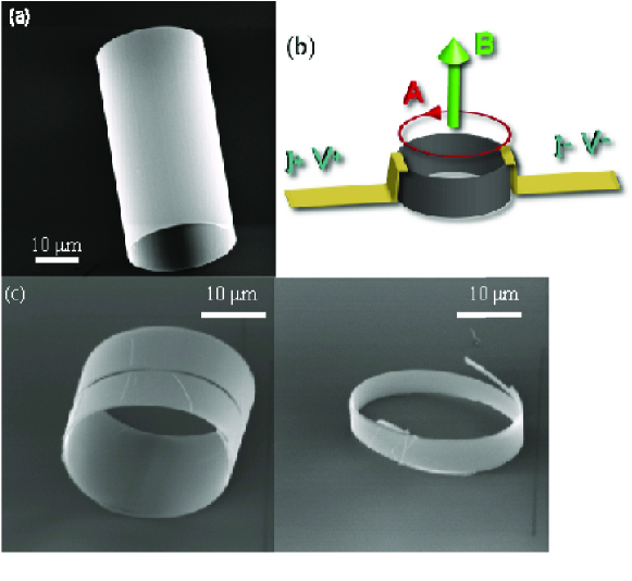
The samples are synthesized by the chemical vapor transportation method Tanda . The materials (tantalum and sulfur) in an evacuated quartz tube react to produce TaS3 crystals (whisker, ring and other kinds of topological crystals). We prepared a ring/tube crystal reproducibly (Figure 1a), and then cut the one with focused ion beam (Figure 1c). The dimensions of the sample are 27 m in diameter and 1 x 0.1 m2 in cross-section area. We fabricated gold electrode on the sample, by electron-beam lithography Inagaki , after coating with polymethylmethacrylate (Figure 1b).
We measured the electric current at 5.1 K while applying a magnetic field to the vertical the ring crystal (Figure 1b). The magnetic field is swept at a sweep rate of 50 mGauss/sec slow enough to eliminate generation of eddy current.
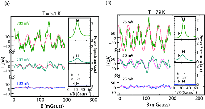
The magnetoresistance of a TaS3 ring crystal is shown at the voltage, 100, 200 and 300 mV, in Figure 2(a). We observed periodic oscillations in these voltages, increasing the amplitude together with the increasing voltage.
We obtained a peak estimated by the power spectra of the observed oscillation. The insets of Figure 2(a) show the evolution of the power spectra, 100, 200 and 300 mV, from bottom to top. The period of the oscillation is 39.7 mGauss for all voltages. By assuming the origin of the oscillation to the AB effect Aharonov ; Webb ; Latyshev , we estimated the effective charge using the following formula,
| (1) |
where is Planck’s constant and is the radius of the ring crystal. The estimated value of an effective charge e∗ is 3.0 x 10⁻¹⁹ C within a 10 percent accuracy and is approximately equal to two times the elementary charge ( = 3.2 x 10⁻¹⁹ C). The red lines in Figure 2(a) show the sinusoidal oscillation with the period and amplitude corresponding to the peak of the power spectra. The major contribution of the observed oscillations is well expressed by the obtained spectra. Other peak, such as or , was not observed within our experiment.
We performed several experiments to confirm reproducibility of our reservation. Changing the sample temperature to 79 K did not show discrepancy in the oscillation period with data at 5.1 K (Figure 2(b)). The insets of Figure 2(b) show the evolution of the power spectra, 25, 50 and 75 mV, from bottom to top. The estimated value of an effective charge e∗ is 3.1 x 10⁻¹⁹ C. Ordinarily, quantum phenomena hide in thermal fluctuation at high temperature by nature, but CDW state shows quantum interference at 79 K, such as superconductor. Moreover, another sample with diameter of 17 m reproduced the same behavior with the period of 95.2 mGauss, which is corresponding to 3.1 x 10⁻¹⁹ C. This periodic oscillation is also nearly equal to .
III Results and Discussion
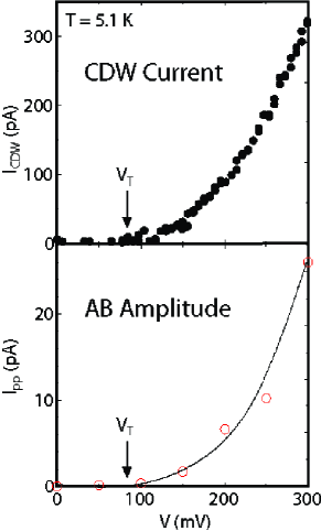
Figure 3 shows the voltage-current characteristics of the sample, after removing an Ohmic (linear) component of the conduction. The CDW current is shown to develop at larger voltage than the threshold . The amplitude of the sinusoidal oscillation at =0 was also plotted in Figure 3 (black line is guide for eyes in bottom panel). In the case of the ordinary fluctuation concerned with free electron, the line becomes linear as a function of the increasing voltage. Figure 3, however, shows that top and bottom curves behave similarly, in particular, a significant increase above . For this reason, the amplitude of the interference is related with sliding CDW. It is plausible to attribute the development of the oscillation to the CDWs.
In addition, the size of the sample is longer than coherent length of a quasi-particle. When a CDW was broken into quasi-particles, they can only stay within the coherence length of CDW. This is understood by analogy with a superconductor. Hence the quasi-particle will not travel over several nanometers, and the coherence of a quasi-particle is unlikely to be preserved over the whole system with the circumference of 85 m at 79 K. The phase correlation length of sliding CDW is longer than quasi-particle and the circumference of our sample because sliding CDW becomes more ordered in the direction of motion Ringland . In case of our sample, the possibility of A’tsuler-Aronov-Spivak effect Latyshev , namely oscillation of a quasi-particle, is ruled out.
Our study shows that the periodicity of CDW is half a flux quantum . Bogachek et al Bogachek suggested that charge quanta of CDWs are multiple of chain number. For example, interference of a single CDW chain results in the period , while a bundle of CDWs with chains provides an oscillation of period. If transverse correlation between CDWs formed CDW bundles, the period of or must be observed. In fact, the power spectra only give the fundamental oscillation.
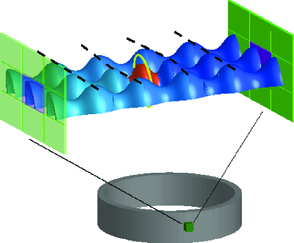
Thus we propose a model to describe the oscillation. Figure 4 shows a schematic picture of a CDW soliton confined into a single chain. A CDW chain (the green wave in Fig. 4) has an extra wavefront, namely a soliton, carrying a charge of Maki . The yellow circle corresponds to a dislocation loop encircling the soliton Duan ; Hatakenaka . Existence of the dislocation loop makes the soliton to move freely along the chain accompanying the charge. This agrees with our observation. Finally, we estimated a mass of CDW condensate, which influences coherence and decoherence in quantum mechanics. The CDWs have large effective mass being 1000 times the electron mass per CDW wavelength as they coupled with phonons and lattice Gruner . In the case of TaS3 ring which has the circumference of 85 m, the effective mass of the single CDW loop is estimated about 108 times electron mass Kagoshima . On the other hand, if a CDW soliton is localized in space, the mass is comparable to the effective mass Arndt . In this context, determination of the model for our observation will directly relate with an applicability of quantum mechanics on macroscopic scales, and solve an important open question in quantum mechanics.
In conclusion, we observed the AB effect at liquid-nitrogen temperature 79 K using a CDW loop of TaS3 ring crystal. The observed period was , which cannot be explained by interference of a quasi-particle. A soliton confined in a CDW chain, possibly originated the oscillation. This work suggests that macroscopic quantum tunneling Bardeen and Fröhlich superconductors Frohlich can occur in sliding CDWs. In principle, the quantum interference of CDWs provides a same sensitivity to an applied magnetic field to that of superconducting quantum interference device. And note that the transition temperatures of CDWs are relatively higher than those of superconductor. Some materials show CDW behavior even at room temperature. Hence our observation will provide a Fröhlich superconducting quantum interference device running at room temperature, which has not been achieved by superconductor.
Acknowledgements.
The authors are grateful to T. Toshima, T. Tsuneta, T. Matsuura, K. Matsuda, K. Ichimura, and K. Yamaya, for experimental support and Y. Asano, M. Hayashi, and N. Hatakenaka for stimulating discussions. This research has been supported by Grant-in-Aid for the 21st Century COE program on gTopological Science and Technology h and the Japan Society for the Promotion of Science.References
- (1) Y. Aharonov and D. Bohm, Phys. Rev. 115, 485-491 (1959).
- (2) A. Tonomura, T. Matsuda, R.Suzuki, A. Fukuhara, N. Osakabe, H. Umezaki, J. Endo, K. Shinagawa, Y. Sugita, and H. Fujiwara, Phys. Rev. Lett. 48, 1443-1446 (1982).
- (3) R. A. Webb, S. Washburn, C. P. Umbach and R. B. Laibowitz, Phys. Rev. Lett. 54, 2696-2699 (1985).
- (4) B. L. Al’tshuler, A. G. Aronov and B. Z. Spivak, JETP Lett. 33, 94-97 (1981).
- (5) Y. Aharonov and A. Casher, Phys. Rev. Lett. 53, 319-321 (1984).
- (6) M. König, A. Tschetschetkin, E. M. Hankiewicz, J. Sinova, V. Hock, V. Daumer, M. Schäfer, C. R. Becker, H. Buhmann, and L. W. Molenkamp, Phys. Rev. Lett. 96, 076804 (2006).
- (7) T. T. Wu and C. N. Yang, Phys. Rev. D 12, 3845-3857 (1975).
- (8) P. A. Horváthy, Phys. Rev. D 33, 407-414 (1986).
- (9) L. H. Ford and A. Vilenkin, J. Phys. A:Math. Gen. 14, 2353-2357 (1981).
- (10) A. Ashtekar and A. Magnon, J. Math. Phys. 16, 341-344 (1975).
- (11) O. Hosten and P. Kwiat, Science 319, 787-790 (2008).
- (12) S. Tanda, T. Tsuneta, Y. Okajima, K. Inagaki, K. Yamaya, and N. Hatakenaka, Nature 417, 397-398 (2002).
- (13) G. Grüner, Density Waves in Solids (Addison-Wesley, Reading, MA, 1994), and references therein.
- (14) E. N. Bogachek, I. V. Krive, I. O. Kulik, and A. S. Rozhavsky, Phys. Rev. B 42, 7614-7617 (1990).
- (15) M. I. Visscher, B. Rejaei, and G. E. W. Bauer, Euro. Lett. 36, 613-618 (1996).
- (16) J. Yi, M. Y. Choi, K. Park, and E.-H Lee, Phys. Rev. Lett. 78, 3523-3526 (1997).
- (17) G. Montambaux, Euro. Phys. Jour. 1, B377-383 (1998).
- (18) Yu. I. Latyshev, O. Laborde, P. Monceau, and S. K. Klaumunzer, Phys. Rev. Lett. 78, 919-922 (1997).
- (19) M. I. Visscher and B. Rejaei, Euro. Phys. Lett. 43, 617-622 (1998).
- (20) T. Matsuura, M. Yamanaka, N. Hatakenaka, T. Matsuyama, and S. Tanda, J. Crys. Grow. 297, 157-160 (2006).
- (21) K. Inagaki, T. Toshima, S. Tanda, K. Yamaya and S. Uji, Appl. Phys. Lett. 86, 073101 (2005).
- (22) K. L. Ringland, A. C. Finnefrock, Y. Li, J. D. Brock, S. G. Lemay, and R. E. Thorne, Phys. Rev. B 61, 4405-4408 (2000).
- (23) K. Maki, Phys. Rev. Lett. 39, 46-48 (1977).
- (24) J.-M. Duan, Phys. Rev. B 48, 4860-4863 (1993).
- (25) N.Hatakenaka, M.Shiobara, K.Matsuda, and S.Tanda Phys. Rev. B 57, R2003-2005 (1998).
- (26) S. Kagoshima, H. Nagasawa, T. Sambongi, One-dimensional Conductors, Springer-Verlag, Berlin (1988).
- (27) M. Arndt, O. Nairz, J. Vos-Andreae, C. Keller, G. van der Zouw and A. Zeilinger, Nature 401, 680-682 (1999).
- (28) J. Bardeen, Phys. Rev. Lett. 42, 1498-1500 (1979).
- (29) H. Fröhlich, Proc. R. Soc. London Ser. A 223, 296-305 (1954).


