Tuning of electron transport through
a quantum wire: An exact study
Santanu K. Maiti†,‡,111Corresponding Author: Santanu K. Maiti
Electronic mail: santanu.maiti@saha.ac.in
†Theoretical Condensed Matter Physics Division,
Saha Institute of Nuclear Physics,
1/AF, Bidhannagar, Kolkata-700 064, India
‡Department of Physics, Narasinha Dutt College,
129 Belilious Road, Howrah-711 101, India
Abstract
We explore electron transport properties in a quantum wire attached to two metallic electrodes. A simple tight-binding model is used to describe the system and the coupling of the wire to the electrodes (source and drain) is treated through Newns-Anderson chemisorption theory. In our present model, the site energies of the wire are characterized by the relation where , , are three positive numbers. For , the threshold bias voltage of electron conduction across the bridge can be controlled very nicely by tuning the strength of the potential . On the other hand, for , the wire becomes an aperiodic one and quite interestingly we see that, for some special values of , the system exhibits a metal-insulator transition which provides a significant feature in this particular study. Our numerical results may be useful for fabrication of efficient switching devices.
PACS No.: 73.23.-b; 73.63.Rt; 73.63.Nm; 85.65.+h
Keywords: Quantum wire; Conductance; DOS; - characteristic; - transition.
1 Introduction
Quantum transport in low-dimensional systems like quantum wires,1-2 quantum wells and quantum dots3-4 provides several novel features due to reduced system dimensionality and lateral quantum confinement. The geometrical sensitivity of such systems makes them truly unique in offering the possibility of studying quantum transport in a very tunable environment. At present, manufacturing of the devices using single molecule or cluster of molecules become more widespread and they provide a signature in the design of future nano-electronic circuits where the electron transport is predominantly coherent.5-6 Based on the pioneering work of Aviram and Ratner7 in which a molecular electronic device has been predicted for the first time, the development of a theoretical description of molecular electronic devices has been pursued. Later, several experiments8-10 have been carried out in different molecular bridges to understand the basic mechanisms underlying such transport. Though electron transport properties through several bridge systems have been investigated elaborately both theoretically as well as experimentally, yet the complete knowledge of conduction mechanism in this scale is not very well established even today. Several significant factors are there which control the electron transport across a bridge system, and all these effects have to be taken into account properly to characterize such transport. For our illustration, here we describe very briefly some of these factors. (i) Molecular coupling to the side attached electrodes and the electron-electron correlation.11 Understanding of the molecular coupling to the electrodes under non-equilibrium condition is a major challenge in this particular study. (ii) Geometry of the molecule itself. To emphasize it, Ernzerhof et al.12 have predicted several model calculations and provided some new interesting results. (iii) Quantum interference effect13-18 of electronic waves passing through the bridge system. (iv) Dynamical fluctuation in small-scale devices is another important factor which plays an active role and can be manifested through measurement of shot noise, a direct consequence of the quantization of charge. It can be used to obtain information on a system which is not available directly through conductance measurements, and is generally more sensitive to the effects of electron-electron correlations than the average conductance.19-20 Beside these factors, several other parameters of the Hamiltonian that describe a system also provide significant effects in the determination of current through a bridge system.
In the present paper, we will investigate the electron transport properties of a quantum wire attached to two semi-infinite one-dimensional (D) metallic electrodes. It is well established from the Bloch’s theorem that, a one-dimensional quantum wire subject to the periodic on-site potentials, exhibits all extended eigenstates. While, for the random distribution of the site potentials, localized states are the only allowed solutions as predicted by the Anderson model.21 Thus, for these two different class of materials we get either all extended states or localized states.21-22 But there is a special type of quasi-random potentials () lying in between the above mentioned potential distributions which have attracted a lot of interest23-34 in last few decays. Our numerical results show that for a special choice of the parameter (), threshold bias voltage of electron conduction across the wire can be controlled in a tunable way by changing the strength of the potential . While for the non-zero value of , the wire becomes an aperiodic one and several interesting results are obtained. Quite significantly we see that, for some particular values of the parameter , the system shows metal-insulator transition which clearly manifests the existence of the mobility edge in conductance spectrum. In our present discussion, we use a simple tight-binding model to incorporate electron transport through a quantum wire, and adopt the Newns-Anderson chemisorption model35-37 for the description of electrodes and for the interaction of electrodes to the wire. Our numerical studies might throw new light, both in the context of basic physics and possible technological applications.
The paper is organized as follows. In Section , we describe the model and methodology for the calculation of transmission probability () and current () through a quantum wire attached to two metallic electrodes using single particle Green’s function formalism. Section discusses the significant results, and finally, we summarize our study in Section .
2 Model and the theoretical description
This section describes the model and technique for the calculation of transmission probability (), conductance () and current () through a quantum wire attached to two D metallic electrodes using the Green’s function method. The schematic view of such a bridge system is illustrated in Fig. 1. In actual experimental set up, these two electrodes made from gold are used and the wire attached to them via thiol groups in the chemisorption technique and in making such contact, hydrogen (H) atoms of the thiol groups remove and the sulfur (S) atoms reside.
For low bias voltage and temperature, conductance of the wire is determined from the Landauer conductance formula,38-39
| (1) |
where, the transmission probability can be written in the form,38-39
| (2) |
where, and correspond to the retarded and advanced Green’s functions of the wire, and and describe the coupling

of the wire to the source and drain, respectively. The Green’s function of the wire is expressed as,
| (3) |
where, is the energy of the injecting electron and corresponds to the Hamiltonian of the wire. Within the non-interacting picture this Hamiltonian can be written in the tight-binding model as,
| (4) |
In this expression, () represents the creation (annihilation) operator of an electron at site , ’s are the on-site energies and corresponds to the nearest-neighbor hopping strength. In our present study, the on-site potentials of the wire are described by the expression,
| (5) |
where, be the strength of the potential and the parameters and are the two other positive numbers define the tight-binding problem. Depending on the value of the parameter , the wire becomes non-aperiodic () or aperiodic (), and both for these two different choices of we get several interesting results. In order to describe the side attached electrodes, viz, source and drain, we use the standard tight-binding Hamiltonian as prescribed in Eq. (4) and parametrized it by constant on-site potential and nearest-neighbor hopping integral . The wire is coupled to these electrodes through the parameters and , where they (coupling parameters) correspond to the coupling strengths to the source and drain respectively. In Eq. (3), the parameters and correspond to the self-energies due to coupling of the wire to the source and drain, respectively. All the information of this coupling are included into these two self-energies and are described by the Newns-Anderson chemisorption model.35-37 This Newns-Anderson model permits us to describe the conductance in terms of the effective wire properties multiplied by the effective state densities involving the coupling, and allows us to study directly the conductance as a function of the properties of the electronic structure of the wire between the electrodes.
The current passing through the wire can be regarded as a single electron scattering process between the two reservoirs of charge carriers. The current-voltage relationship can be obtained from the expression,38
| (6) |
where gives the Fermi distribution function with the electrochemical potential . Usually, the electric field inside the wire, especially for small wires, seems to have a minimal effect on the - characteristics. Thus it introduces very little error if we assume that, the entire voltage is dropped across the wire-electrode interfaces. The - characteristics are not significantly altered. On the other hand, for larger system sizes and higher bias voltage, the electric field inside the wire may play a more significant role depending on the size and structure of the wire,40 though the effect is quite small.
All the results presented in this communication are worked out for zero temperature. However, they should remain valid even in a certain range of finite temperature ( K). This is due to the fact that the broadening of energy levels of the wire due to the electrode-wire coupling is, in general, much larger than that of the thermal broadening.38 For simplicity, we take the unit in our present calculations.
3 Numerical results and discussion
This section demonstrates the transport properties of a quantum wire. Here we concentrate our results on clarifying the dependence of conductance and current on (i) the parameters , and and (ii) the coupling strength of the wire
to the two side attached electrodes. The parameter is an irrational number which is set to , for our illustration. Out of these three parameters (, , ), is the most significant one. For the three distinct regimes of , we get several important results which we will discuss here one by one. In the first regime, . Therefore, the on-site energy () alternates between the two values and . Thus the wire becomes a non-aperiodic one. The other two regimes are and , where we choose and , respectively. In the same footing, the wire-to-electrode coupling strength has a strong dependence in the transport phenomena. To reveal this fact, here we focus our results for the two distinct regimes, the so-called weak- and strong-coupling regimes, respectively. These two regions are described by the conditions and , respectively. The values of these parameters for the two distinct regimes are taken as: , (weak-coupling) and , (strong-coupling). Throughout the calculations, the on-site
potential and hopping integral in the electrodes are set as and , respectively. The equilibrium Fermi energy is fixed at .
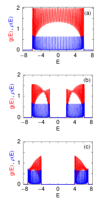
To illustrate our results, let us first concentrate to the regime where . As representative examples, the characteristic properties of the conductance (red color) and density of states (DOS) (blue color) for some typical quantum wires are presented in Fig. 2, where (a), (b) and (c) correspond to , and , respectively. For this particular value of , the wire becomes a non-aperiodic one and the on-site energies become or depending on whether the site index is even or odd. Figure 2(a) represents the result for a completely perfect wire where all the site energies are set to zero (as for this particular case). The conductance shows sharp resonant peaks throughout the bandwidth of the wire ( to ), associated with the energy eigenvalues of it. This is clearly observed by superposing the picture of the density of states on the conductance profile. At these resonances, the conductance gets the value , and accordingly,
the transmission probability becomes unity, since from the Landauer conductance formula the relation holds (see Eq. (1) with in our present description). Thus the conductance spectrum manifests itself the electronic structure of the system. In Figs. 2(b) and (c), the results are shown for the finite values of , and quite interestingly we see that, a gap appears in the conductance spectra across the energy . This is due to the existence of the two energy bands separated by twice the width of disorder. Therefore, the gap between the two bands increases with the increase of the strength , which is clearly observed from these figures. Thus we can tune the electron conduction across the wire by controlling the parameter . This provides an interesting phenomenon, and it can be much more clearly understood from our study of the current-voltage (-) characteristics.
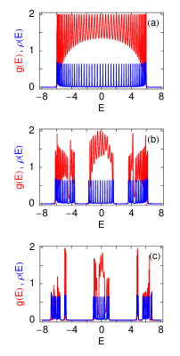
Now we consider the results for the aperiodic quantum wires where becomes finite. As illustrative examples, in Fig. 3, we display the conductance and density of states for some typical aperiodic
quantum wires, where (a), (b) and (c) correspond to , and , respectively. For these wires, we set . When , the result is exactly similar to that as given in Fig. 2(a). We re-plot this result once again to compare the other results for the finite values of quite clearly. Our numerical results show that, for this particular regime of (), the conductance spectrum breaks into three distinct regions associated with the DOS spectrum. Quite significantly it is observed that, the energy separation between these bands increases with the strength of . Thus we get three separate energy bands for these kind of aperiodic quantum wires. Such a behavior can be used to construct multiple switching devices, which is really a very interesting observation in the transport community.
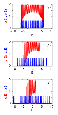
The most significant result is obtained when we choose i.e., in the regime . As representative examples, we plot the - and - characteristics in Fig. 4 for some typical aperiodic quantum wires subject to this particular value of , where (a), (b) and (c) correspond to , and , respectively. Figure 4(a) is identical with those as in Fig. 2(a) and Fig. 3(a). For non-zero values of , Figs. 4(b)
and (c) clearly show that there are eigenstates existing in the energy regimes for which the conductance is completely zero. This illustrates the transition from the conducting (high ) to the non-conducting or insulating phase, the so-called metal-insulator transition in the system. Thus from the conductance and the DOS spectra, a crossover from a completely opaque to a fully transmitting zone is easily understood. In view of such a crossover, one can then set the Fermi energy at a suitable energy zone in the spectrum and control the transmission characteristics. This enhances the prospect of such quantum wires as novel switching devices.
Up to now, all the results studied here are described only for the strong-coupling limit. Quite similar feature will also be observed in the conductance spectra for the weak-coupling limit in these three distinct regimes of . The only difference appears in the conductance spectra in these two coupling limits is that, in the weak-coupling case the widths of the resonant peaks become much narrow than that of the strong-coupling case. This broadening solely depends on the imaginary parts of the two self-energies and .38 Now for these quantum wires, since we get many resonant peaks, it is quite difficult to observe the difference between the widths of the resonant peaks in the conductance spectra for the two different coupling cases, and therefore, we do not show the results for the weak-coupling case. The effects of the electrode-wire coupling can be much more clearly understood from the current-voltage characteristics which we are going to discuss in our forthcoming parts of this paper.
Current across the bridge is computed from the integration procedure of the transmission function as prescribed in Eq. (6). The transmission function varies exactly similar to that of the conductance spectra as illustrated above, differ only in magnitude by the factor since the relation holds from the Landauer conductance formula (Eq. (1)). Let us first discuss the results for the case . As typical examples, in Fig. 5, we plot the current-voltage (-) characteristics for some non-aperiodic quantum wires (), where the st, nd and rd rows correspond to , and , respectively. The red lines represent the results for the weak-coupling limit, while the blue lines denote the results in the limit of strong-coupling. Both for these two limiting cases several significant results are observed. In the weak wire-electrode coupling, the current exhibits staircase-like structure with fine steps as a function of the applied bias voltage. This is due to the existence of the sharp resonant peaks in the conductance spectra in this limit of coupling, since current is computed by the integration method of the transmission function . With the increase of the applied bias voltage, electrochemical potentials on the electrodes are shifted gradually, and finally cross one of the quantized energy levels of the wire. Therefore, a current channel is opened up and the current-voltage characteristic curve provides a jump. On the other hand, for the strong wire-electrode coupling, current varies almost continuously with the applied bias voltage and achieves much large amplitude than the weak-coupling case. This is because the resonant peaks get broadened due to the broadening of the energy levels in the strong-coupling limit which provide much larger current amplitude as we integrate the transmission function to get the current. Thus by tuning the wire-to-electrode coupling, one can achieve very high current from the very low one. Now the effect of
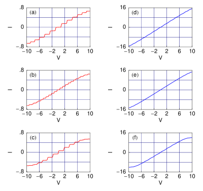
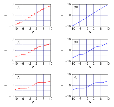
is quite interesting in this particular study. For the non-zero value of , current across the wire is obtained beyond some finite bias voltage (see Figs. 5(b) and (e)), which is associated with the conductance and DOS spectra (Fig. 2). This threshold bias voltage increases with the increase of the strength (see Figs. 5(c) and (f)). Thus one can shift the threshold bias voltage gradually by changing the parameter accordingly.
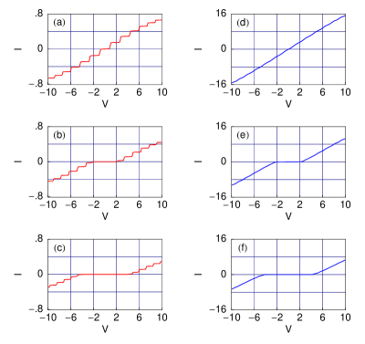
Next we make an attention to the current-voltage characteristics for the aperiodic quantum wires where we set . In Fig. 6, we represent the current-voltage characteristics for some aperiodic quantum wires, where the st, nd and rd rows correspond to , and , respectively. The red and blue curves represent the identical meaning as in Fig. 5. Both for the weak- and strong-coupling cases, we get quite similar features as in the case i.e, step-like in the limit of weak-coupling and continuous-like in the other limiting case. But the key behavior is that, here one gets the current across the wire for much low bias voltage in the weak coupling case, while in the strong wire-electrode coupling the current is available as long as the bias voltage is applied. In the presence of , an interesting behavior is observed. Our results show that, for a wide range of the applied bias voltage, the current remains constant and after that it again increases with the voltage . This constant current region can also be controlled by tuning the appropriate parameters.
Finally, we consider the particular case where we fix . The results are shown in Fig. 7, where the st, nd and rd rows correspond to the similar strengths of as in the previous cases. The red and blue curves also represent the identical meaning as above. The coupling effects are same as described earlier. For this particular value of , the current is observed for any non-zero value of in both these two limiting cases as long as the bias voltage is applied (see the nd and rd rows of Fig. 7). Like in Fig. 6, here we will also get the saturation region of the current that appears at quite higher values of the bias voltage , which is not shown here in the figure. This saturation region continues with the bias voltage and there is no such possibility of getting the current further for the higher voltages as in the case of .
4 Concluding remarks
In conclusion, the electron transport properties in a quantum wire attached to two semi-infinite D metallic electrodes have been investigated by using the single particle Green’s function formalism. We have used a simple tight-binding model to describe the system where the coupling of the wire to the electrodes has been treated through the Newns-Anderson chemisorption theory. In this article, we have described our results for the three typical values of those are associated with the three different regimes of this parameter. For , the wire becomes a non-aperiodic one and in such a case, the threshold bias voltage of electron conduction can be tuned significantly by controlling the strength of the potential . On the other hand, for the non-zero value of , the wire becomes an aperiodic one and several other key features are obtained. In the regime , conductance spectrum breaks into three separate bands associated with the energy spectrum. By tuning the parameter , we can change the gap between the bands in the conductance spectrum, which is responsible for the constant current across the wide range of applied bias voltage. The most remarkable result is observed in the regime . In this regime (), our numerical results have shown a cross over from the conducting (high ) to non-conducting or insulating phase. This illustrates a metal-insulator transition in the system. In view of such a crossover, one can tune the Fermi energy to a suitable energy zone in the spectrum, and thus, can be able to control the transmission properties. This aspect may be utilized in designing a tailor made switching device. In this article we have also described the effects of the wire-electrode coupling which have been clearly visible from our current-voltage characteristics. The current shows sharp staircase-like structure in the weak-coupling limit, while it varies quite continuously and achieves very high value in the limit of strong-coupling. Thus, we can emphasize that, care should be taken on the coupling effects in fabrication of electronic circuits by using nano-scale systems.
Throughout our discussions we have used several approximations by neglecting the effects of the electron-electron interaction, all the inelastic scattering processes, the Schottky effect, the static Stark effect, etc. Beside these, here we have also made another one approximation by calculating all the results at absolute zero temperature, and we have already stated about it at the end of Section . Instead of calculating all the results at zero temperature, we can also determine these results at some finite temperatures. But, our presented results will not change significantly even for some finite non-zero temperatures. More studies are expected to take into account all these approximations for our further investigations.
Acknowledgments
I acknowledge with deep sense of gratitude the illuminating comments and suggestions I have received from Prof. Arunava Chakrabarti and Prof. Shreekantha Sil during the calculations.
References
- [1] P. A. Orellana, M. L. Ladron de Guevara, M. Pacheco, and A. Latge, Phys. Rev. B 68, 195321 (2003).
- [2] P. A. Orellana, F. Dominguez-Adame, I. Gomez, and M. L. Ladron de Guevara, Phys. Rev. B 67, 085321 (2003).
- [3] S. M. Cronenwett, T. H. Oosterkamp, and L. P. Kouwenhoven, Science 281, 5 (1998).
- [4] A. W. Holleitner, R. H. Blick, A. K. Huttel, K. Eber, and J. P. Kotthaus, Science 297, 70 (2002).
- [5] A. Nitzan, Annu. Rev. Phys. Chem. 52, 681 (2001).
- [6] A. Nitzan and M. A. Ratner, Science 300, 1384 (2003).
- [7] A. Aviram and M. Ratner, Chem. Phys. Lett. 29, 277 (1974).
- [8] T. Dadosh, Y. Gordin, R. Krahne, I. Khivrich, D. Mahalu, V. Frydman, J. Sperling, A. Yacoby, and I. Bar-Joseph, Nature 436, 677 (2005).
- [9] J. Chen, M. A. Reed, A. M. Rawlett, and J. M. Tour, Science 286, 1550 (1999).
- [10] M. A. Reed, C. Zhou, C. J. Muller, T. P. Burgin, and J. M. Tour, Science 278, 252 (1997).
- [11] T. Kostyrko and B. R. Bułka, Phys. Rev. B 67, 205331 (2003).
- [12] M. Ernzerhof, M. Zhuang, and P. Rocheleau, J. Chem. Phys. 123, 134704 (2005).
- [13] R. Baer and D. Neuhauser, Chem. Phys. 281, 353 (2002).
- [14] R. Baer and D. Neuhauser, J. Am. Chem. Soc. 124, 4200 (2002).
- [15] D. Walter, D. Neuhauser, and R. Baer, Chem. Phys. 299, 139 (2004).
- [16] K. Tagami, L. Wang, and M. Tsukada, Nano Lett. 4, 209 (2004).
- [17] M. Magoga and C. Joachim, Phys. Rev. B 59, 16011 (1999).
- [18] K. Walczak, Cent. Eur. J. Chem. 2, 524 (2004).
- [19] Y. M. Blanter and M. Buttiker, Phys. Rep. 336, 1 (2000).
- [20] K. Walczak, Phys. Stat. Sol. (b) 241, 2555 (2004).
- [21] P. W. Anderson, Phys. Rev. 109, 1492 (1958).
- [22] P. A. Lee and T. V. Ramakrishnan, Rev. Mod. Phys. 57, 287 (1985).
- [23] S. Das Sarma, S. He, and X. C. Xie, Phys. Rev. B 41, 5544 (1990).
- [24] S. Das Sarma, A. Kobayashi, and R. E. Prange, Phys. Rev. Lett. 56, 1280 (1986).
- [25] S. Das Sarma, A. Kobayashi, and R. E. Prange, Phys. Rev. B 34, 5309 (1986).
- [26] S. Das Sarma, S. He, and X. C. Xie, Phys. Rev. Lett. 61, 2144 (1988).
- [27] D. R. Grempel, S. Fishman, and R. E. Prange, Phys. Rev. Lett. 49, 833 (1982).
- [28] J. B. Sokoloff, Phys. Rep. 126, 189 (1985).
- [29] M. Kohmoto, L. P. Kadanoff, and C. Tang, Phys. Rev. Lett. 50, 1870 (1983).
- [30] M. Griniasty and S. Fishman, Phys. Rev. Lett. 60, 1334 (1988).
- [31] S. Aubry and G. André, in Group Theoretical Methods in Physics, edited by L. Horwitz and Y. Neeman, Annals of the Israel Physical Society Vol. 3 (American Institute of Physics, New York, 1980), p. 133.
- [32] C. M. Soukoulis and E. N. Economou, Phys. Rev. Lett. 48, 1043 (1982).
- [33] M. Johansson and R. Riklund, Phys. Rev. B 42, 8244 (1990).
- [34] M. Johansson and R. Riklund, Phys. Rev. B 43, 13468 (1991) .
- [35] D. M. Newns, Phys. Rev. 178, 1123 (1969).
- [36] V. Mujica, M. Kemp, and M. A. Ratner, J. Chem. Phys. 101, 6849 (1994).
- [37] V. Mujica, M. Kemp, A. E. Roitberg, and M. A. Ratner, J. Chem. Phys. 104, 7296 (1996).
- [38] S. Datta, Electronic transport in mesoscopic systems, Cambridge University Press, Cambridge (1997).
- [39] M. B. Nardelli, Phys. Rev. B 60, 7828 (1999).
- [40] W. Tian, S. Datta, S. Hong, R. Reifenberger, J. I. Henderson, and C. I. Kubiak, J. Chem. Phys. 109, 2874 (1998).