Universal zero-bias conductance for the single electron transistor. II: Comparison with numerical results
Abstract
A numerical renormalization-group survey of the zero-bias electrical conductance through a quantum dot embedded in the conduction path of a nanodevice is reported. The results are examined in the light of a recently derived linear mapping between the temperature-dependent conductance and the universal function describing the conductance for the symmetric Anderson model. A gate potential applied to the conduction electrons is known to change markedly the transport properties of a quantum dot side-coupled to the conduction path; in the embedded geometry here discussed, a similar potential is shown to affect only quantitatively the temperature dependence of the conductance. As expected, in the Kondo regime the numerical results are in excellent agreement with the mapped conductances. In the mixed-valence regime, the mapping describes accurately the low-temperature tail of the conductance. The mapping is shown to provide a unified view of conduction in the single-electron transistor.
pacs:
73.23.-b,73.21.La,72.15.Qm,73.23.HkI Introduction
The development of the first single-electron transistor (SET)Goldhaber-Gordon et al. (1998a) was preceded by analytical and numerical breakthroughsGlazman and Raikh (1987); Ng and Lee (1988); Hershfield et al. (1991); Meir and Wingreen (1992); Wingreen and Meir (1994); Costi et al. (1994) and, in the subsequent years, motivated numerous theoretical investigations.W. et al. (1998); Hofstetter et al. (2001); Aguado and Langreth (2003); Franco et al. (2003); Pustilnik and Glazman (2004); Zitko and Bonca (2006); Nisikawa and Oguri (2006); Maruyama et al. (2004); Romeike et al. (2006); Dias da Silva et al. (2006); Bulla et al. (2008) Notwithstanding this intense activity, important aspects of the transport properties of the device received limited attention. In particular, even after it guided the interpretation of experimental data drawn out of nanodevices,Goldhaber-Gordon et al. (1998b); Cronenwett et al. (2002); Sato et al. (2005); Katsumoto et al. (2006) the concept of universality remained confined to the narrow corner in which it was first identified.Costi et al. (1994)
As it was established much more recently, in the Kondo regime of the Anderson model,Anderson (1961) the thermal dependence of the zero-bias conductance of quantum dots either embeddedYoshida et al. (2009) in or side-coupledSeridonio et al. (2009) to the conduction path of elemental nanodevices maps linearly onto the conductance curve for the symmetric model computed by Costi, Hewson and Zlatic.Costi et al. (1994) The linear coefficient in the mapping, which is parametrized by the ground-state phase shift of the conduction electrons to which the quantum dot is coupled, depends on the geometry. Qualitatively different thermal dependences result, which distinguish the side-coupled geometry from the embedded configuration. With a side-coupled quantum dot, the linear coefficient depends only on the phase shift. As it results, the application of a potential to the conduction electrons can switch the conductance curves from monotonically increasing to monotonically decreasing functions of the temperature.Seridonio et al. (2009)
In the embedded configuration, of which the SET is the simplest illustration, the conductance always decreases with temperature. The mapping depends on the difference between the ground-state phase shift and the phase shift that the potential would induce if the conduction electrons were decoupled from the dot. In the special class of model Hamiltonians that are invariant under particle-hole transformations, the symmetry makes the dot occupation unitary, and it follows from the Friedel sum ruleLangreth (1966) that . For asymmetric Hamiltonians, by contrast, a priori knowledge of is impossible. In the Kondo regime, again on the basis of the Friedel sum rule, a difference close to is expected;Yoshida et al. (2009) accurate estimates nevertheless require diagonalization of the model Hamiltonian. One possibility would be to generate temperature-dependent conductance curves from Bethe-ansatzAndrei et al. (1983); Tsvelick and Wiegmann (1983) results for the phase shift. Here, however, we prefer the numerical renormalization-group (NRG) approach, which gives direct access to the phase shifts and to the thermal dependence of the conductance.
This paper compares numerically computed SET conductances with the mapping to the universal function. From the same NRG diagonalization of the model Hamiltonian, we compute (i) the conductance as a function of the temperature; and (ii) the ground-state phase shift, which specifies the mapping. Plotted as functions of the temperature in the Kondo regime, the computed conductances rise from from nearly zero to nearly ballistic as decreases past the Kondo temperature, and conduction electrons screen the the dot magnetic moment. The curves obtained from the mapping run through the numerical data.
Outside the Kondo domain, the mapping to the univeral function is expected to fail. To witness its downfall, the numerical survey includes the adjacent mixed-valence domain, in which the dot moment is only partially formed. Here, the conductance crosses over to its ground-state value at relatively high temperatures, which are outside the domain of the mapping; hence, only the low-temperature tail of the numerical data can be accurately fitted.
Our presentation is distributed over five Sections. Section II describes the SET and the Anderson Hamiltonian modeling it. Section III discusses cursorily the mapping derived in Ref. Yoshida et al., 2009. Section IV is dedicated to the NRG procedure, which it summarizes, and to the numerics, which it details. The numerical results appear next, in Section V, which starts with a discussion of the phase-shift differences .
The same section presents the conductance curves. Besides describing quantitatively the conductance in the Kondo regime (and the low-temperature sector of the mixed-valence regime), the mapping to the universal function offers a simple, unifying view of charge transport through a single-electron transistor. Faithful to this notion, Sections V.1 and V.2 compound the output of 100 NRG runs in two plots of the conductance as a function of the temperature and gate potential applied to the quantum dot; and show that every feature of the landscapes is easily understood in the light of that mapping. Section V.3 then turns the numerically computed ground-state phase shifts into linear coefficients, and the mapping into conductance curves that fit the NRG results for the temperature-dependent conductances. Our conclusions and a summary constitute the closing Section VI.
II Model
Figure 1 depicts the object of our study, a quantum dot symmetrically coupled to two otherwise independent quantum wires. The tunneling amplitude transfer charge between the dot and the wires. To represent the dot, we introduce a single, spin-degenerate level . An energy , controlled by the gate potential , and a Coulomb repulsion define the dot Hamiltonian , which can be writtenKrishna-murthy et al. (1980b)
| (1) |
to emphasize that the energy breaks the particle-hole symmetry of the dot Hamiltonian.

Inclusion of the quantum wires, represented by a structureless half-filled band of width containing conduction states, and of their coupling to the quantum dot yields the Anderson Hamiltonian
| (2) |
where
| (3) |
and is the potential due to the wire electrodes in Fig. 1.
The coupling , to the wires, broadens the dot level . The scattering potential reduces its width , where is the density of conduction states, toYoshida et al. (2009)
| (4) |
With , a specially important instance of Eq. (2) is the particle-hole symmetric Hamiltonian
| (5) |
to which reduces for .
The operators on the right-hand side of Eq. (2) are even combinations of the conduction operators in the left and in the right wire segments in Fig. 1: . The inversion symmetry of the device decouples the odd combinations from the dot level, which make no explicit contribution to the zero-bias conductance . Linear Response relates to the dot-level spectral density :Yoshida et al. (2009)
| (6) |
where is the quantum conductance, is the Fermi function, is the partition function for the Hamiltonian , and
| (7) |
Here, () denotes an eigenstate of with eigenvalue ().
The substitution of Eq. (7) on the right-hand side of Eq. (6) yields an expression that translates into a few lines of computer code:
| (8) |
As this expression suggests, the computational efforts underlying a conductance curve and e. g., a magnetic susceptibility plotKrishna-murthy et al. (1980a) are comparable.
III Mapping
Equation (8) yields conductances ranging from zero to the quantum conductance . We are interested in the Kondo regime, the vast parametric subspace defined by the condition and . At the high-temperature end of the Kondo regime a magnetic moment arises, associated with the nearly unitary dot-level occupancy . As the temperature is lowered past the Kondo temperature , and the wire electrons screen the resulting dot magnetic moment, the Kondo cloud couples the dot level to the wire states and sustains conductance. Costi, Hewson and ZlaticCosti et al. (1994) showed that the thermal dependence of the conductance for the symmetric Hamiltonian (5) is a universal function of the temperature scaled by the Kondo temperature. More recently, we have shown that the Kondo-regime conductance maps linearly onto :Yoshida et al. (2009)
| (9) |
where is the ground-state conduction-band phase shift, and , the Fermi-level phase shift for , i. e.,
| (10) |
As the temperature rises, the universal function decays from , through , to . The linear coefficient on the right-hand side of Eq. (9) is a function of the phase-shift difference . It follows from the Friedel sum rule that , so that in the Kondo regime, and even in the mixed-valence regime, is never small. According to Eq. (9), for , the conductance sticks to . A particular case is the symmetric Hamiltonian (5), for which , , and . If the difference were , on the other hand, the conductance would be flat: . For the intermediate differences observed in the Kondo and mixed-valence regimes, the conductance is a monotonically decreasing function of the temperature. If , is smaller than the quantum conductance, is nonzero, and is flatter than .
IV Numerics
Excellent descriptions of the NRG method being available,Krishna-murthy et al. (1980a); Hewson (1993); Bulla et al. (2008) brief recapitulation of the four steps constituting the procedure will be sufficient. Two dimensionless parameters and define the logarithmic discretization of the conduction band.Yoshida et al. (1990); Bulla et al. (2008) The infinite energy sequence () defines the intervals . For each interval, a single operator , with normalization factor , is defined. In the negative half of the conduction band, the sequence () defines the mirror image of each operator . The forma a basis upon which the conduction band Hamiltonian is projected.Krishna-murthy et al. (1980a)
Next, a Lanczos transformationKomzsik (2003) makes tridiagonal the projected conduction Hamiltonian, so that the model Hamiltonian reads
| (11) |
Here, is the operator defined in Eq. (3), and the ’s () form an orthonormal basis that replaces the ’s (). With , we recover the Lanczos transformation in Ref. Krishna-murthy et al., 1980a. Otherwise, the codiagonal coefficients have to be determined numerically.Yoshida et al. (1990) With error , it is foundCampo and Oliveira (2005) that . This shows that the ’s decrease rapidly with , a conclusion that brings us to the third step in the NRG procedure, the definition of a renormalization-group transformation.
Given a temperature and a small dimensionless parameter , let be the smallest integer such that , and consider the infinite sum on the right-hand side of Eq. (11). Compared to , the codiagonal element is then negligible, and to compute , it is safe to neglect the term with . This decouples the subsequent terms in the sum from the quantum dot, so that they no longer contribute to the conductance. The infinite sum can therefore be truncated at . We define the reduced bandwidth and the dimensionless, scaled, truncated Hamiltonian :
| (12) |
The entire Hamiltonian has been divided by so that the smallest codiagonal coefficient in the scaled sum, , is of .
The last step in the NRG procedure is the iterative diagonalization of the model Hamiltonian. With , the right-hand side of Eq. (12) is easily diagonalized; four eigenvalues and four eigenvectors () result. At this stage, it is equally simple to calculate the matrix elements between the eigenvectors of , which will be needed to compute the right-hand side of Eq. (8).
Application of the operators , , , and the identity on the eigenvectors of generates sixteen states that constitute a basis upon which the Hamiltonian can be projected. Appropriately chosen linear combinations of those operators yield basis states () that diagonalize the charge and spin operators; projected on them, reduces to block-diagonal matrices, which are then diagonalized numerically. The matrix elements () are projected onto the basis and subsequently rotated to the basis of the eigenstates () of . Application of the operators , , , and on the creates 64 basis vectors upon which can be projected, and the procedure is iterated.
To check the exponential growth of matrix dimensions, a dimensionless parameter is chosen, which will control the cost and the accuracy of the iterative diagonalization. At the end of iteration , the eigenvectors with scaled energies above are discarded before the construction of the basis states , upon which the Hamiltonian will be projected. This expedient limits the number of basis states and hence the computational effort that each iteration requires. The cost of a full NRG run grows linearly with the number of iterations.
The diagonalization yields scaled eigenvalues ranging from unity to , i. e., a window of energies ranging from to . Having neglected , we can only compute conductances for , where . At the other extreme, the ultraviolet truncation restricts us to temperatures such that . Thus, provided that , i. e., that , the -th iteration yields reliable conductances in the temperature window . If a run is stopped at iteration , the juxtaposition of the resulting windows yields for all temperatures above . In practice, the conductance is only computed for the , because irrelevant operators artificially introduced by the logarithmic discretization make the interval unreliable.
Conductance curves computed with large show oscillations, which can be traced to a sequence of poles on the lines of the complex-energy plane.Yoshida et al. (1990) To eliminate these artifacts of the discretization, we average the conductance curve computed for given over a sequence of equally spaced ’s in the interval .Wanda C. Oliveira and Luiz N. Oliveira (1994) The exponential deependence of the computational effort on , makes this averaging procedure far more efficient than comparably accurate computations with small .
The conductances in Section V were computed with and averaged over two ’s: 0.5 and 1. The amplitude of the residual oscillations encountered after averaging over , somewhat smaller than , provides an estimate of the error introduced by the logarithmic discretization. The other two parameters controlling the precision of the results were fixed at and , respectively. Spin degeneracies not counted, the number of states below the cutoff in each iteration peaked at 4000 in iteration 6. To estimate the error due to the infrared and ultraviolet truncations, for each we compared the conductance at the lowest temperature in the ()-th window, , with the conductance at the highest temperature in the -th window. The mismatch between the two results never exceeding , we conclude that deviations due to the three approximations in the procedure, the logarithmic discretization and the infrared and ultraviolet truncations, are comparable. At any temperature, the estimated absolute deviation in the computed conductances is smaller than than of the quantum conductance.
The relatively large discretization parameter expedites the calculation. On a standard desktop computer, a complete run, including (i) the iterative diagonalization of and computation of the matrix elements on the right-hand side of Eq. (8) for for each , and (ii) the evaluation of the conductance curve in the interval , takes less than 30 seconds.
Phase shifts
Along with the iterative diagonalization procedure, Eq. (12) defines a renormalization-group transformation:Krishna-murthy et al. (1980a)
| (13) |
The factor multiplying the first term on the right-hand side magnifies the scale on which the eigenvalues of are examined. On the new scale, the second term is a fine structure. In the absence of characteristic energies, as grows the magnification compensates the refinement, and the lowest-energy eigenvalues of rapidly become indistinguishable from those of . This indicates that the Hamiltonian has reached a fixed point of .
In the Kondo regime, the condition turns the Anderson Hamiltonian into the local-moment fixed point (LM) of . With , as the temperature is reduced past the dominant characteristic energy , the Hamiltonian first approaches the LM and then moves away towards the frozen-level fixed point (FL)—a strong-coupling fixed point equivalent to Eq. (2) with . Between the LM and the FL lies the Kondo temperature , around which the conduction electrons screen the dot moment.
If one of the dot excitation energies, or , is smaller than the dot width , the model Hamiltonian enters the mixed-valenc regime.111Ref. Krishna-murthy et al., 1980b discusses the mixed-valence regime under the heading “transitional cases”, in Section III.E. Instead of , the dominant characteristic energy is now . The dot moment is only partially formed, as the coupling drives the model Hamiltonian toward the FL before it can come close to the LM.
Devoid of characteristic energies, the two fixed points, LM and FL, are phase-shifted conduction bands, which can be diagonalized analytically.Krishna-murthy et al. (1980b) With , for instance, the model Hamiltonian flows towards the LM with phase shift . With , (inaccurate) estimates for the LM phase shifts can be extracted from the eigenvalues of , where is such that , i. e., such that the model Hamiltonian dwells in the vicinity of the LM.
Much more accurate FL phase shifts can be obtained from the low-energy eigenvalues of , because for large the eigenvalues of come arbitrarily close to the many-body excitations of the FL HamiltonianKrishna-murthy et al. (1980b); Yoshida et al. (2009)
| (14) |
Here, the and subscripts distinguish the positive eigenvalues from the negative ones, while counts the positive (negative) eigenvalues upward (downward) from the Fermi level.
Once the eigenvalues of are identified with the many-body energies generated from Eq. (14), the ground-state phase shift are extracted from the approximate expression describing all but the closest to zero.Krishna-murthy et al. (1980b) For , in particular, within deviation,
| (15) |
where () for odd (even) .
V Results
To emulate the conditions under which a SET operates, we fix the Coulomb repulsion () and effective dot-level width () and examine the ground-state phase shift and the thermal dependence of the conductance as a function of the dot energy for five wire potentials . Since , , and are invariant under the transformation , , , , we need not study negative wire potentials, which would mirror the conductances and phase shifts calculated with positive .
We turn first to the calculated phase shifts. Figure 2 displays the argument of the trigonometric function on the right-hand side of the mapping (9), computed for five wire potentials , in the dot-energy range . For , the upright triangles draw a well-known curve,Tsvelick and Wiegmann (1983) which remains invariant under the particle-hole transformation , . At the symmetric point , which corresponds to Eq. (5), the phase-shift is exactly . The arrows above the top axis indicate the Kondo domain, within which the phase shift remains close to . As grows, the model Hamiltonian first approaches the limits of the Kondo domain and then invades the mixed-valence domain. In response, moves away from , towards zero for , or towards for .
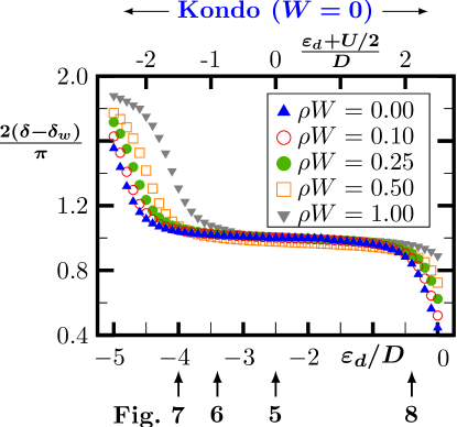
The wire potential reduces the ground-state phase shift throughout the depicted range. For , for instance, the phase shift at the symmetric dot-level energy is reduced from to . In the Kondo-regime, as the illustration shows, the difference is nonetheless pinned at . The pinning is due to the Friedel sum rule.Langreth (1966) Since the ground-state phase shift would be if were zero, is the screening charge due to the coupling to the dot. In the Kondo regime, that charge is nearly unitary, and .
Figure 2 shows that a positive wire potential tends to displace the Kondo regime towards higher dot energies. For , the rapid decay of the phase shift near () marks the resonance between the and ( and ) dot-level configurations. The Kondo regime lies between them. As grows, the two resonances move to higher ’s, and so does the Kondo regime.
V.1 Conductance landscape
According to Eq. (9), controls . Consequently, the central features of Fig. 2 are manifest in landscape plots of the conductance. Figure 3 shows in the dot-energy range for , and . The plot surveys the entire Kondo regime and part of the mixed-valence regime. The plane , which represents the symmetric Hamiltonian (5), splits the landspace in two symmetric halves, mapped onto each other by the particle-hole transformation , .
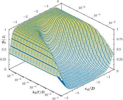
Examined at the symmetric point , the temperature-dependent conductance reproduces the universal function . Here and elsewhere in the Kondo regime, the conductance at fixed rises from zero to ballistic or nearly ballistic as the temperature is reduced past , i. e., as one climbs from the high-temperature Coulomb-blockade valley to the low-temperature Kondo plateau. The Kondo temperature for the symmetric Hamiltonian is . As grows, it rises until , an equality indicating proximity to the mixed-valence regime, i. e., to the two resonances centereced at and . As grows further, we come into mixed-valence domain. The dot moment shrinks, and so does the Kondo cloud. The Kondo bypass of the Coulomb blockade becomes less and less effective, and the conductance approaches zero. The steep drops near the and planes in Fig. 3 mark the mixed-valence regime.
V.2 Wire potential
Figure 4 displays the conductance as a function of and for , , and . Quantitative differences distinguish the plot from Fig. 3. In particular, the Kondo temperature is now minimized at the higher dot-level energy , the minimum is thirtyfold higher, the resonance between the and dot configurations is now centered at , and the resonance between the and dot configurations has been reduced to an incipient rise, at the high- end of the plot. Clearly, the wire potential has displaced the Kondo domain towards higher dot-level energies. This displacement acknowledged, we recognize in Fig. 4 the salient features of Fig. 3.
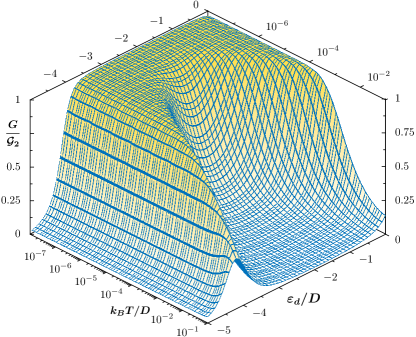
The two landscapes are similar because the phase-shift difference on the right-hand side of Eq. (9) is weakly dependent on . With , the conductance curve is approximately mapped onto throughout the Kondo domain. The rise from the high-temperature valley to the Kondo plateau is therefore close to universal, dependent on the model parameters only through the Kondo temperature . The latter is a function of the antiferromagnetic interaction between the dot moment and the conduction electrons around it. The Schrieffer-Wolff transformationSchrieffer and Wolff (1966) relates that interaction to the dot excitation energies:
| (16) |
Here, () is the energy needed to remove (add) and electron to the singly-occupied dot level. For the symmetric Hamiltonian (5), in particular, . For nearly symmetric Hamiltonians, and . As or grow, the resulting particle-hole asymmetry renormalizes the dot energy,Haldane (1978); Krishna-murthy et al. (1980b) so that and are changed to and , respectively, where is the effective dot energy at the LM.Krishna-murthy et al. (1980b)
Since both landscapes were computed for the same effective width , only (i) the excitation energies and ; and (ii) irrelevant operators make the Kondo temperatures in Fig. 3 different from those in Fig. 4. The renormalized excitation energies displace the Kondo domain along the axis, while the modified irrelevant operators extend the Kondo plateau towards higher temperatures.
V.3 Thermal dependence of the conductance
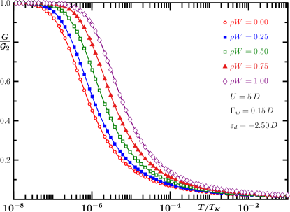
Figure 5 displays the conductance as a function of the temperature for , , , and five wire potentials: and , already studied in Figs. 3 and 4, and three intermediate values, , 0.5, and 0.75. With , the open circles represent the symmetric Hamiltonian (5), and the solid line through them reproduces the universal function computed in Ref. Costi et al., 1994. Notwithstanding the wire potentials, the Hamiltonians represented by the squares, triangles, and diamonds lie deep inside the Kondo regime. For each of them, the phase-shift difference in Table 1 is close to . It follows that the right-hand side of Eq. (9) is close to . The agreement with the numerical data is excellent.
| Figure | Symbol | |||||
|---|---|---|---|---|---|---|
| 5 | 0.00 | 0.00 | 0.50 | 1.00 | 8.1 | |
| 5 | 0.25 | -0.21 | 0.29 | 1.00 | 1.1 | |
| 5 | 0.50 | -0.32 | 0.18 | 1.01 | 2.0 | |
| 5 | 0.75 | -0.37 | 0.13 | 1.01 | 3.4 | |
| 5 | 1.00 | -0.40 | 0.11 | 1.02 | 6.0 | |
| 6 | 0.00 | 0.00 | 0.51 | 1.02 | 4.4 | |
| 6 | 0.25 | -0.21 | 0.30 | 1.03 | 1.1 | |
| 6 | 0.50 | -0.32 | 0.20 | 1.03 | 3.6 | |
| 6 | 0.75 | -0.37 | 0.15 | 1.05 | 1.1 | |
| 6 | 1.00 | -0.40 | 0.13 | 1.06 | 3.6 | |
| 7 | 0.00 | 0.00 | 0.52 | 1.04 | 8.8 | |
| 7 | 0.25 | -0.21 | 0.32 | 1.06 | 3.3 | |
| 7 | 0.50 | -0.32 | 0.23 | 1.10 | 1.6 | |
| 7 | 0.75 | -0.37 | 0.22 | 1.17 | 7.3 | |
| 7 | 1.00 | -0.40 | 0.25 | 1.31 | 3.4 * | |
| 8 | 0.00 | 0.00 | 0.42 | 0.84 | 7.7 | |
| 8 | 0.25 | -0.21 | 0.24 | 0.90 | 2.4 | |
| 8 | 0.50 | -0.32 | 0.15 | 0.93 | 9.4 | |
| 8 | 0.75 | -0.37 | 0.10 | 0.95 | 4.0 | |
| 8 | 1.00 | -0.40 | 0.08 | 0.96 | 1.9 |
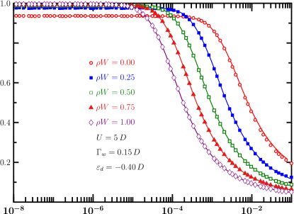
As the Hamiltonian moves away from the plane, the particle-hole asymmetry becomes more pronounced. One might expect the difference to grow. As Fig. 2 showed, however, in the Kondo regime the Friedel sum rule restrains the growth, so that . Illustrative results appear in Fig. 6, which displays conductance curves for . Even for the strongest wire potential in the legend, , the difference in Table 1 is only 6% away from . As in Fig. 5, therefore, the conductance curves computed from Eq. (9) are close to . The agreement with the numerical data is again flawless. Since we are now closer to the boundary of the Kondo regime, the Kondo temperature is more sensitive to the renormalization of the dot-level energy induced by strong wire potentials. Compared to Fig. 5, Fig. 6 thus exhibits a substantially broader spread of crossover temperatures.
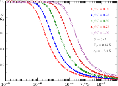
Figure 7 displays numerical results for , a still larger departure from the symmetric condition. For , the agreement with Eq. (9) is excellent; for , it is imperfect only at the highest temperatures shown. For , however, there is substantial disagreement, which justifies a digression.
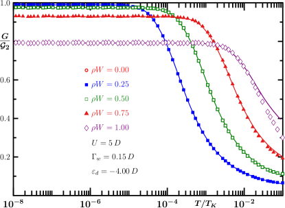
Inspection of Fig. 4 shows that, for (and ), the model Hamiltonian lies well within the mixed-valence regime.222With and , although in the mixed-valence regime, the model Hamiltonian is close to the Kondo regime. In the Kondo regime, Eq. (9) is reliable for thermal energies that are small on the scale of the dominant characteristic energy . If had its bare value, , the mapping would be reliable for . The dot energy has been renormalized, however, and the renormalization has pushed the model Hamiltonian into the mixed-valence regime. The dominant characteristic energy has therefore been changed to , a reduction that restricts the domain of the mapping to . The mapping fails at higher temperatures because irrelevant operators, which are sizable near the characteristic energy, make a significant contribution to the conductance. At , for example, the diamonds in Fig. 7 are displaced below the solid line; upon cooling, decays in proportion to and becomes insignificant below .
If were steadily increased beyond , the model Hamiltonian would traverse the mixed-valence region. Once , the dot occupation would approach . The dominant characteristic energy would then define the crossover energy scale, which would hence rise with . Soon, the model Hamiltonian would be driven to the frozen-level fixed point at the first steps of the renormalization-group flow, and the mapping would be reduced to its FL limit, .
Although Eq. (9) is asymptotically exact at low temperatures, i. e., for , as our digression showed its practical value is eroded outside the Kondo regime. In the mixed-valence regime, in particular, the asymptotic region lies below the crossover temperature, i. e., in the vicinity of the FL. To plot the rightmost solid line in Fig. 7, we thus had to match the right-hand side of Eq. (9) to the diamond at , because the identification , which defined for all the other plots in Figs. 5-8, became unreliable for . The asterisk in Table 1 marks the resulting Kondo temperature.
Near the opposite extreme of the Kondo regime, for fixed, small , the wire potential drives the model Hamiltonian toward the center of the Kondo regime. In Fig. 4, for instance, the mixed-valence domain is missing, because the wire potential displaced it to positive dot-level energies. Figure 8 displays the plane for the five potentials , 0.25, 0.5, 0.75, and 1. The Hamiltonian is now at the boundary of the Kondo regime, and for , irrelevant operators introduce significant deviations from the solid line. As grows, however, the model Hamiltonian sinks deeper into the Kondo regime, and the agreement with the solid lines is recovered.
VI Conclusions
In the Kondo regime, the physical properties for the Anderson model are universal functions of the temperature scaled by the Kondo temperature. The conductance constitutes no exception. For , the Anderson Hamiltonian reduces to Eq. (5), in which case the thermal dependence of the SET conductance is the universal function .Costi et al. (1994); Bulla et al. (2008) For nonzero or , Eq. (9) maps linearly the conductance onto .Yoshida et al. (2009) With , the particle-hole symmetry of the Hamiltonian (5) forces the ground-state phase shift to be and reduces Eq. (9) to a trivial identity. For asymmetric Hamiltonians in the Kondo regime, as the 5th and 6th columns in Table 1 and the plots in Fig. 2 suggest, while the ground-state phase shift can take any value in its domain of definition, the Friedel sum rule keeps the difference close to . The linear coefficient of the mapping (9) is never far from , and the thermal dependence of the SET conductance, never far from .
Equation (9) becomes asymptotically exact as . In the Kondo regime, the dominant characteristic energy is , and the mapping to the conductance is reliable throughout the crossover from the LM to the FL. In the mixed-valence regime, with or , the dominant characteristic energy reduces the domain of the universal mapping to a temperature range close to the low-temperature fixed point, i. e., to the final steps in the rise to the limit .Seridonio et al. (2009)
Summary
To recapitulate, the essentially exact numerical data in Figs. 2-8 offer an overview of electrical conduction through a quantum dot embedded in the conductance path of a nanostructured device. The linear mapping (9) to the universal function for the symmetric Anderson HamiltonianCosti et al. (1994); Bulla et al. (2008) describes accurately the thermal dependence of the conductance for in the Kondo regime. A gate potential applied to the wires affects only quantitatively the dependence of the conductance on the temperature and dot-level energy.
In the Kondo regime, independently of the wire potential, the Friedel sum rule drives the thermal dependence of the conductance to the neighborhood of . In particular, . In the mixed-valence regime, only well below the crossover temperature does map onto , and is substantially smaller than the quantum conductance. In the laboratory, it is often difficult to distinguish the Kondo regime from the mixed-valence regime. Goldhaber-Gordon et al. (1998b); Sato et al. (2005) The mapping to the universal curve offers a practical solution to this problem.
Acknowledgements.
This work was supported by the CNPq and FAPESP.References
- Goldhaber-Gordon et al. (1998a) D. Goldhaber-Gordon, H. Shtrikman, D. Mahalu, D. Abusch-Magder, U. Meirav, and M. A. Kastner, Nature 391, 156 (1998a).
- Costi et al. (1994) T. Costi, A. Hewson, and V. Zlatic, Journal of Physics–Condensed Matter 6, 2519 (1994).
- Glazman and Raikh (1987) L. I. Glazman and M. E. Raikh, JETP Lett. 47, 452 (1987).
- Ng and Lee (1988) T. K. Ng and P. A. Lee, Phys. Rev. Lett. 61, 1768 (1988).
- Hershfield et al. (1991) S. Hershfield, J. H. Davies, and J. W. Wilkins, Phys. Rev. Lett. 67, 3720 (1991).
- Meir and Wingreen (1992) Y. Meir and N. S. Wingreen, Phys. Rev. Lett. 68, 2512 (1992).
- Wingreen and Meir (1994) N. S. Wingreen and Y. Meir, Phys. Rev. B 49, 11040 (1994).
- Bulla et al. (2008) R. Bulla, T. A. Costi, and T. Pruschke, Rev. Mod. Phys. 80, 395 (2008), ISSN 0034-6861.
- W. et al. (1998) I. W., S. O., and S. Y., J. Phys. Soc. Jpn. 67, 2444 (1998).
- Hofstetter et al. (2001) W. Hofstetter, J. König, and H. Schoeller, Phys. Rev. Lett. 87, 156803 (2001).
- Aguado and Langreth (2003) R. Aguado and D. C. Langreth, Phys. Rev. B 67, 245307 (2003).
- Franco et al. (2003) R. Franco, M. S. Figueira, and E. V. Anda, Phys. Rev. B 67, 155301 (2003).
- Zitko and Bonca (2006) R. Zitko and J. Bonca, Phys. Rev. B 73, 035332 (2006).
- Nisikawa and Oguri (2006) Y. Nisikawa and A. Oguri, Phys. Rev. B 73, 125108 (2006).
- Maruyama et al. (2004) I. Maruyama, N. Shibata, and K. Ueda, J. Phys. Soc. Japan 73, 3239 (2004).
- Romeike et al. (2006) C. Romeike, M. R. Wegewijs, W. Hofstetter, and H. Schoeller, Phys. Rev. Lett. 96, 196601 (pages 4) (2006).
- Dias da Silva et al. (2006) N. P. Sandler, K. Ingersent, and S. E. Ulloa, Phys. Rev. Lett. 97, 096603 (pages 4) (2006).
- Pustilnik and Glazman (2004) M. Pustilnik and L. Glazman, J. Phys. Cond. Matter 16, R513 (2004).
- Goldhaber-Gordon et al. (1998b) D. Goldhaber-Gordon, J. Gores, M. A. Kastner, H. Shtrikman, D. Mahalu, and U. Meirav, Phys. Rev. Lett. 81, 5225 (1998b).
- Sato et al. (2005) M. Sato, H. Aikawa, K. Kobayashi, S. Katsumoto, and Y. Iye, Phys. Rev. Lett. 95, 066801 (2005).
- Cronenwett et al. (2002) S. M. Cronenwett, H. J. Lynch, D. Goldhaber-Gordon, L. P. Kouwenhoven, C. M. Marcus, K. Hirose, N. S. Wingreen, and V. Umansky, Phys. Rev. Lett. 88, 226805 (2002).
- Katsumoto et al. (2006) S. Katsumoto, M. Sato, H. Aikawa, and Y. Iye, Physica E: Low-dimensional Systems and Nanostructures 34, 36 (2006).
- Anderson (1961) P. W. Anderson, Phys. Rev. 124, 41 (1961).
- Yoshida et al. (2009) M. Yoshida, A. C. Seridonio, and L. N. Oliveira, Universal zero-bias conductance for the single-electron transistor (2009), URL http://www.citebase.org/abstract?id=oai:arXiv.org:0906.4063.
- Seridonio et al. (2009) A. C. Seridonio, M. Yoshida, and L. N. Oliveira, Europhys. Lett., to be published (2009), URL http://www.citebase.org/abstract?id=oai:arXiv.org:cond-mat/07%01529.
- Langreth (1966) D. C. Langreth, Phys. Rev. 150, 516 (1966).
- Tsvelick and Wiegmann (1983) A. M. Tsvelick and P. B. Wiegmann, Advances in Physics 32, 453 (1983).
- Andrei et al. (1983) N. Andrei, K. Furuya, and J. H. Lowenstein, Rev. Mod. Phys. 55, 331 (1983).
- Krishna-murthy et al. (1980a) H. R. Krishna-murthy, J. W. Wilkins, and K. G. Wilson, Phys. Rev. B 21, 1003 (1980a).
- Hewson (1993) A. C. Hewson, The Kondo Problem to Heavy Fermions (Cambridge University Press, Cambridge, 1993).
- Yoshida et al. (1990) M. Yoshida, M. A. Whitaker, and L. N. Oliveira, Phys. Rev. B 41, 9403 (1990).
- Komzsik (2003) L. Komzsik, The Lanczos Method: Evolution and Application (SIAM, Philadelphia, 2003).
- Campo and Oliveira (2005) V. L. Campo and L. N. Oliveira, Phys. Rev. B 72, 104432 (2005).
- Wanda C. Oliveira and Luiz N. Oliveira (1994) Wanda C. Oliveira and Luiz N. Oliveira, Phys. Rev. B 49, 11986 (1994).
- Krishna-murthy et al. (1980b) H. R. Krishna-murthy, J. W. Wilkins, and K. G. Wilson, Phys. Rev. B 21, 1044 (1980b).
- Schrieffer and Wolff (1966) J. R. Schrieffer and P. A. Wolff, Phys. Rev. 149, 491 (1966).
- Haldane (1978) F. D. M. Haldane, Phys. Rev. Lett. 40, 416 (1978).