The role of background impurities in the single particle relaxation lifetime of a two-dimensional electron gas
Abstract
We re-examine the quantum and transport scattering lifetimes due to background impurities in two-dimensional systems. We show that the well-known logarithmic divergence in the quantum lifetime is due to the non-physical assumption of an infinitely thick heterostructure, and demonstrate that the existing non-divergent multiple scattering theory can lead to unphysical quantum scattering lifetimes in high quality heterostructures. We derive a non-divergent scattering lifetime for finite thickness structures, which can be used both with lowest order perturbation theory and the multiple scattering theory. We calculate the quantum and transport lifetimes for electrons in generic GaAs-AlGaAs heterostructures, and find that the correct ‘rule of thumb’ to distinguish the dominant scattering mechanisms in GaAs heterostructures should be for background impurities and for remote impurities. Finally we present the first comparison of theoretical results for and with experimental data from a GaAs 2DEG in which only background impurity scattering is present. We obtain excellent agreement between the calculations and experimental data, and are able to extract the background impurity density in both the GaAs and AlGaAs regions.
pacs:
72.20.Dp, 72.10.-d, 73.63.-bI Introduction
Over the past four decades, an enormous effort has been dedicated to developing two-dimensional electron gases (2DEGs) engineered at the interface of semiconductor heterostructures, and optimising their low temperature transport properties Ando et al. (1982); Pfeiffer and West (2003). It is now possible to achieve low temperature mobilities in excess of in high quality GaAs-AlGaAs heterostructures Pfeiffer et al. (1989); Umansky et al. (1997), and there is continued interest in further improving 2DEG mobilities Umansky et al. (in press). Phenomena that are only observed in ultra-high mobility 2DEGs include anisotropies, stripe and bubble phases in higher Landau levels Lilly et al. (1999), microwave induced resistance oscillations Mani (2004), and even denominator fractional quantum Hall states Willett et al. (1987). The latter have attracted considerable interest due to proposals for topological quantum computers that use the possible non-abelian nature of the fractional quantum Hall state Sarma et al. (2005). Since these even denominator fractional quantum Hall states are only observed in ultra-high mobility 2DEGs at very low temperatures (), there is renewed interest in understanding the factors limiting the electron mobility in GaAs heterostructures Hwang and Sarma (2008).
The maximum attainable electron mobility is limited by phonon scattering, which cannot be avoided. However for low temperatures, K, phonon scattering is negligible, and the mobility is limited by other mechanisms. In GaAs heterostructures these include interface roughness scattering, remote ionised impurity scattering, and background impurity scattering. Interface roughness scattering is not important in high quality heterointerfaces at low densities, so the low mobility is limited by ionised impurity scattering Gottinger et al. (1988); Bockelmann et al. (1990). In most two-dimensional GaAs systems the carriers are introduced by modulation doping of the AlGaAs, and this modulation doping provides a significant source of remote ionised impurity scattering Dingle et al. (1978). Remote ionised impurity scattering can be reduced with the use of large undoped AlGaAs ‘spacer’ layers between the 2DEG and the modulation doping Störmer et al. (1981), or eliminated entirely with accumulation mode devices in which the carriers are introduced electrostatically rather than through doping Kane et al. (1993). Finally there are always ‘background impurities’ incorporated in the crystal during the epitaxial growth process, and these will limit the mobility in both the very cleanest modulation doped samples Umansky et al. (1997) and in electrostatically doped samples.
In practice, experimentally determining the factors limiting the mobility in a particular sample is non-trivial, since many scattering mechanisms may be acting together. There are two key experimental parameters available to try and separate the different scattering mechanisms: The transport scattering time , obtained from the conductivity, and the single-particle relaxation time (also known as the quantum lifetime) , obtained from the Shubnikov-de Haas oscillations. For short range isotropic scattering the two times are equivalent (e.g. in silicon MOSFETs), but for long range Coulomb interactions (e.g. from modulation doping) and are quite different Harrang et al. (1985); Sarma and Stern (1985); Coleridge et al. (1989). The difference lies in the fact that counts all scattering events, while is weighted towards large-angle scattering events that cause a significant change in the momentum. By comparing the measured and with numerical calculations it is possible to determine the nature of the predominant scattering mechanism in a 2DEG at low temperatures Sarma and Stern (1985); Kearney et al. (2000); Harrang et al. (1985); Coleridge et al. (1989). This is particularly important for background impurity scattering in ultra-high mobility 2D systems, since the impurity levels are so low that they cannot be measured by direct tools such as deep level transient spectroscopy.
While the transport scattering rates can be calculated using first order perturbation theory for a variety of scattering mechanisms, direct comparison between experimental measurements and theoretical calculations of and in high mobility samples have been limited by a problem in calculating the single-particle relaxation time for background impurity scattering: There is no lowest order result for the single-particle relaxation time for homogeneous background doping due a divergent integral Gold (1988). In a series of papers, Gold and Götze extended the theoretical formalism to include multiple scattering effects in both the transport and single-particle cases Gold (1988); Gold and Götze (1986, 1981). This made it possible to calculate the ‘renormalized’ single-particle lifetime for scattering from homogeneous background impurities Gold (1988).
In this paper we re-examine the scattering lifetime due to background impurities, and explicitly highlight how the logarithmic divergence in is due to the assumption of an infinitely thick heterostructure in Refs. Gold (1988); Davies (2000). We derive a non-divergent scattering lifetime for a finite thickness heterostructure, both in the lowest order perturbation theory approach and in the multiple scattering theory. Comparing these two approaches shows how the existing multiple scattering theory can lead to inaccurate scattering lifetimes in high quality heterostructures. Finally we present the first comparison of theoretical results for and with experimental data from a GaAs 2DEG with only background impurity scattering. We obtain excellent agreement between the calculations and experimental data, and are able to extract the background impurity density in both the GaAs and AlGaAs regions.
The remainder of this paper is structured as follows: In Section II we review the standard concepts and expressions for ionised impurity scattering in a 2DEG, with special emphasis on homogenous background scattering, and introduce the correct expression for background impurity scattering in a finite thickness sample. In Section III we evaluate these expressions for background impurity scattering, and compare the different approaches to calculating the single particle and quantum lifetimes. In Section IV we compare our results with experimental data, followed by conclusions in Section V.
II Theory
We restrict our analysis to 2DEGs at , and concentrate on re-examining how the scattering lifetimes are calculated for background impurity scattering, since other scattering mechanisms are readily treated with first order perturbation theory Gold (1988); Davies (2000). Most GaAs-AlGaAs heterostructures share a common layer structure, as shown in Fig. 1: a GaAs substrate/buffer with AlGaAs layer(s) above, and the 2DEG accumulated at the heterointerface. The AlGaAs layer may contain remote ionised impurities, as in the conventional modulation doped HEMT shown in Fig. 1(a), or may be undoped as in ‘induced’ field effect devices (Fig. 1(b)). The heterostructure in Fig. 1(b) has no modulation doping to form the 2DEG – instead the degenerately doped GaAs cap acts as a metallic gate, and carriers are induced by electrostatic doping with a gate bias Solomon et al. (1984); Kane et al. (1993). For the purposes of evaluating background impurity scattering, both types of heterostructure can be treated as consisting essentially of two layers: A GaAs substrate below the 2DEG of thickness , and AlGaAs layers on top of thickness Footnote 1 (2009).

II.1 Background Impurity Scattering in the Lowest Order Theory
In the lowest order of approximation, the transport and single-particle scattering lifetimes and are calculated at by integrating the scattering potential with respect to the scattered wavevector :
| (1) | |||||
| (2) |
Equations (1) and (2) can be derived via Fermi’s Golden Rule or by invoking the second Klauder approximation to the self-energy , where the formalism is presented in Gold (1988). Here is the electron effective mass (taken as for GaAs) and is the Fermi wave vector, which in two-dimensional reciprocal space is a measure of the radius of the mass-shell at . We use the Thomas-Fermi approximation to the dielectric function :
| (3) |
The dielectric function includes the form factor to account for the finite width of the 2DEG, where is a variational parameter and defines the thickness of the 2DEG Fang and Howard (1966).
Equations (1) and (2) show that the magnitudes of and are related to the scattering potential , which is characterized by both the type of disorder and geometry of the quantum well that confines the 2DEG. To calculate the scattering from homogenous background impurities it is necessary to divide the bulk sample into infinitesimal layers, and treat each layer as a -doped layer of remote ionized impurities at a distance from the 2DEG. The scattering potential due to one of these -doped layers is:
| (4) |
Here is the two-dimensional impurity density in the -doped layer and is the form factor that accounts for the finite thickness of the 2DEG. There are two form factors, and , for scattering sites located in the AlGaAs and GaAs regions respectively Footnote 2 (2009):
| (5) |
The difference between the two form factors is due to the overlap between the wave function of the 2DEG and the background impurities in the GaAs region.
The total scattering potential is obtained by summing the contribution from all of the delta-layers:
| (6) | |||||
to obtain:
| (7) |
The three-dimensional background impurity density is now defined by .
Equations (1)–(7) represent the standard lowest order expression for scattering from background impurities. Eqn. (1) is well behaved, but Eqn. (2) diverges as and cannot be evaluated.
The divergence in for background impurity scattering arises from the infinite limits in Eqn. (6), which physically corresponds to an infinite sample, containing an infinite number of charged impurities located far from the 2DEG. These charged background impurities, most of which are located far from the 2DEG, lead to a divergence in the small angle (small ) scattering rate due to the term in Eqn. (4), and hence to a divergence in . However the transport lifetime is convergent since it is less sensitive to small angle scattering events. The non-physical assumption of an infinitely thick sample has been a common assumption in previous calculations of background impurity scattering Gold (1989, 1990, 1985); Kearney et al. (2000); Davies (2000).
To solve the problem of the logarithmic divergence in the single-particle scattering rate, it is tempting to simply modify the lower limit of the integral in Eqn. (2) and replace it with the uncertainty of the 2D scattered wave vector . However, there are several problems with this approach. First of all, the integrand in Eqn. (2) contributes most strongly near the two limits of integration. Thus the result of the integral is extremely sensitive to any modifications of these two limits. Secondly one requires a precise knowledge of all the physical constraints that specify the uncertainty in regarding the system of interest. The uncertainty in will depend on some of the same parameters that affect the scattering rate that one intends to calculate. Only an approach which addresses the problem self-consistently would allow one to be confident of the results. Thirdly even if one can remove the logarithmic divergence with this approach, there still exists the assumption that the heterostructure is infinitely thick. This assumption is not only physically unsound, but also produces inaccurate results as we demonstrate in Section III.
II.2 The Single-Particle Lifetime in the Higher Order Theory
The conventional way around the logarithmic divergence in the integral for is to use the multiple scattering theory developed by Gold to calculate the renormalized single-particle scattering lifetime Gold (1988). The starting point for incorporating multiple scattering effects into the single-particle lifetime is to use the single-particle Green’s function with the mass-shell and third Klauder approximations Gold (1988); Klauder (1961). Taking into account only electron-impurity interactions (i.e. neglecting electron-electron interactions) one arrives at the following expression for :
| (8) | |||||
Eqn. (8) is a self-consistent equation with a double integral that must be solved recursively to obtain . This is a somewhat involved, and computationally intensive, operation and so has rarely (if ever) been used to model experimentally obtained single-particle scattering lifetimes. It is possible to simplify equation (8) by carrying out analytical approximations as in Ref. Gold (1988), but this introduces significant deviations from the exact result, particularly for low disorder GaAs-AlGaAs heterostructures MacLeod et al. (2007).
Kearney et al. showed that the double integral of equation (8) can be reduced to a single integral through contour integration Kearney et al. (2000):
| (9) |
where is given by:
Equation (9) allows the renormalised single particle relaxation time for background scattering for an infinitely thick heterostructure to be calculated efficiently (in a few minutes) using a standard personal computer. To demonstrate this we evaluate as a function of the carrier density for a generic 2DEG in a GaAs-AlGaAs heterostructure (c.f. Fig. 1), for three different background impurity densities, as shown in Fig. 2. The scattering lifetime decreases with decreasing carrier density, although it tends to saturate slightly at low densities. Unlike the lowest order scattering times and , the self-consistent nature of means that it is not a simple linear function of the background impurity density: Increasing by a factor of 10 does not simply reduce by a factor of 10.

II.3 A Physically Realistic Scattering Potential for Homogeneous Background Impurities
Although Fig. 2 provides convergent results for the single-particle lifetime due to background impurity scattering, it is instructive to identify the source of the divergence that caused problems for the lower order theory in the first place. It is a simple exercise to correct the background scattering potential and set a realistic thickness for the heterostructure, with finite bounds on the integrals in Eqn. (6). This leads to the potential:
| (10) | |||||
Here and are the thickness and background doping levels in the AlGaAs layer above the 2DEG, and and are the thickness and background doping levels in the GaAs layer below the 2DEG. Using the scattering potential in Eqn. (10) the lowest order single particle relaxation time can now be calculated without divergence. This scattering potential can also be used in Eqn. (9) to calculate the renormalised for a sample with finite thickness.
III Evaluation of theoretical scattering times
Having removed the divergence in the calculation of the single particle scattering lifetime, we can now evaluate and compare the various lifetimes for different sample thicknesses and doping levels.
III.1 A Comparison of , and
In Figure 3 we plot the scattering lifetimes evaluated for the generic GaAs-AlGaAs heterostructure of Fig. 1 as a function of sample thickness, for three different background impurity concentrations. For these calculations we have taken the background impurity levels in the GaAs and AlGaAs regions to be the same . We also set the thickness of the two regions to be the same , so that the total sample thickness is . The electron effective mass is taken as , and the dielectric constant of both GaAs and AlGaAs as .
The solid line in Fig. 3 shows the transport relaxation time as a function of sample thickness, for three different levels of the background doping density . As the sample is made thicker there are more and more background impurities for electrons to scatter from, and decreases. Above nm the scattering rate saturates, since background impurities located more than 100 nm from the 2DEG essentially act as remote impurities, predominantly causing small angle scattering that does not affect the momentum.
The dashed line in Fig. 3 shows the lower order single-particle lifetime , calculated using Eqn. (10). The single particle lifetime now produces convergent results, and like it decreases as the sample becomes thicker (larger ). The single particle scattering time is always shorter than the equivalent transport scattering time, since counts all scattering events and is weighted towards large angle scattering events. However exhibits the non-physical behaviour of continually decreasing as the thickness is increased, so that even impurities located at an almost infinite distance contribute to the scattering, and the single particle scattering rate diverges as . Even though can now be calculated for real samples, it cannot safely be used to obtain the ratio for comparison with experiments, since is always sensitive to the thickness of the sample, and it overestimates the scattering compared to the higher order . Note that since and are calculated to lowest order, the scattering rate is directly proportional to , so the solid and dashed curves in the three panels of Fig. 3 differ only by a numerical prefactor ().
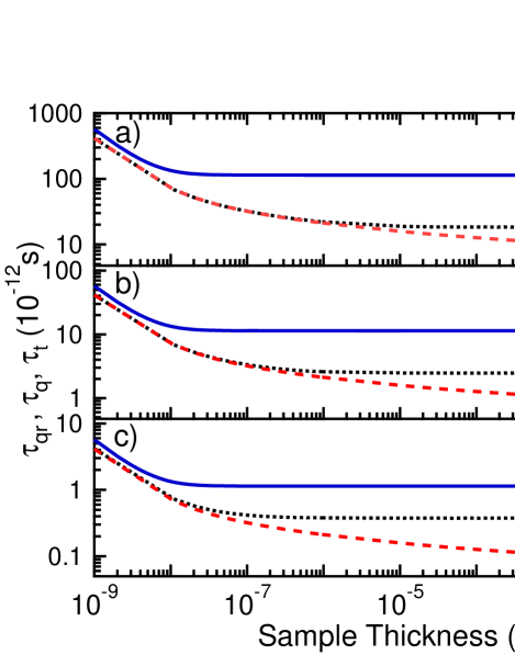
The crosses in Fig. 3 show the renormalised single particle scattering time , calculated using the higher order multiple scattering theory in Eqn. (9). As originally defined by Gold Gold (1988), this scattering time is evaluated for an infinitely thick sample, yet produces a convergent result. Since the renormalised scattering time is calculated iteratively ( exists on both the left and right sides of Eqn. (9)), is not a simple function of ; increasing tenfold does not necessarily increase by a factor of ten.
It is instructive to examine how the renormalised scattering time behaves for finite thickness samples, using the finite thickness scattering potential (Eqns. (9) and (10)). The dotted lines in Fig. 3 show calculated as a function of sample thickness. The renormalised single-particle lifetime saturates to a finite value, , as the thickness of the sample is increased, although it takes longer to saturate than the transport scattering time. The dotted lines in Figs. 3(a-c) also show that as the background impurity density is increased, saturates at a smaller sample thickness. Physically this indicates that the ‘dirtier’ a sample is, the less effect impurities situated away from the 2DEG have on the scattering of electrons in the 2DEG.
The calculations of for finite thickness samples also highlight a problem with clean samples that are thinner than m, such as heterostructure epilayers: hasn’t yet saturated to , so the standard assumption of an infinite heterostructure thickness Gold (1989, 1990, 1985); Kearney et al. (2000) results in an overestimation of the renormalised single-particle scattering rate . This result clearly demonstrates that the scattering potential must take into account the finite thickness of the heterostructure for accurate comparison with experimental data.
Since the GaAs and AlGaAs layers in a real sample are generally not of equal thickness (typically the AlGaAs region is nm and the GaAs region is ), it is useful to investigate how quickly saturates in each layer as a function of the layer thickness. However since is calculated recursively and self-consistently through Eqn. (9), Matthieson’s rule no longer holds, and the scattering rates for the two regions cannot be calculated independently of each other. We therefore have to calculate for the complete sample, and then determine the fraction of the total scattering caused by each layer. To do this was calculated for GaAs and AlGaAs layers having the same thickness and doping levels, . After was obtained for the entire sample, this value of was inserted into the right hand side of Eqn. (9), with the appropriate choice of for either the AlGaAs or GaAs region, to obtain the scattering from each layer individually. The results are plotted in Fig. 4 as a function of the layer thickness . The calculated scattering times show that there are two significant differences between the single-particle lifetime for the AlGaAs and GaAs regions: (i) Most of the contribution to the total scattering lifetime comes from impurities in the GaAs region; (ii) The scattering contribution from the GaAs saturates faster than that from the AlGaAs region as is increased. Physically this means that most of the scattering in the GaAs region comes from impurities close to the channel (), whereas in the AlGaAs region impurities located a considerable distance from the 2DEG can still cause appreciable scattering. The results in Fig. 4 again highlight the problem with the conventional assumption of an infinite sample thickness when calculating , since in most heterostructures the AlGaAs epilayer is only a few hundred nm thick yet doesn’t saturate to the infinite limit until .

III.2 Comparison of and
It is widely assumed that the ratio of the transport to the single particle lifetime can be taken as an indication of the dominant scattering mechanism Sarma and Stern (1985); Kearney et al. (2000); Harrang et al. (1985); Coleridge et al. (1989). The conventional wisdom is that should be close to 1 for background impurity scattering and much larger than 1 for remote ionised impurity scattering. To test if this is correct we plot in Fig. 5 both and calculated for background impurity scattering only, as a function of the 2D carrier density. We take the ‘generic’ thicknesses of the heterostructure to be for the AlGaAs region and for the GaAs region, with three different background doping levels () varied from .
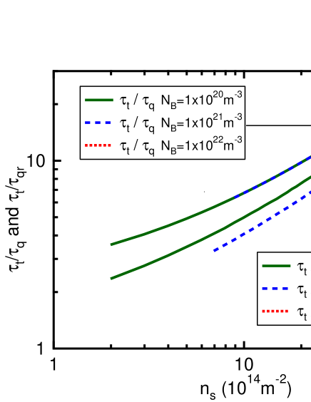
In Fig. 5 the calculation is performed for a finite sample, so the lowest order single particle scattering time is convergent and both and can be evaluated. There is no self-consistency in the lowest order theory (the impurity concentration is effectively just a prefactor in the integrals in Eqns. (1) and (2)), so is insensitive to . In contrast decreases as is increased, indicating that there is proportionally more large angle scattering as the background impurity density is increased.
The key result of Fig. 5 is that even for background impurity scattering alone can be as high as 10, which is much larger than conventional wisdom would suggest. We suggest instead that the correct ‘rule of thumb’ to distinguish the dominant scattering mechanisms in GaAs heterostructures should be for background impurity and for remote ionised impurity scattering MacLeod et al. (2007).
IV Comparison with experimental data
We now compare our results with experimental data from a 2DEG in a GaAs-AlGaAs heterojunction. This sample is specially designed to only have background impurity scattering, to allow direct comparison between experiment and theory. The sample has no modulation doping to form the 2DEG – instead carriers are induced by electrostatic doping with a gate bias (this type of sample is referred to as a Semiconductor Insulator Semiconductor FET, SISFET Solomon et al. (1984), or Heterostructure Insulated Gate FET, HIGFET Zhu et al. (2003)). The sample consists of a 450 substrate, 1 GaAs, 160nm AlGaAs and 60nm GaAs cap. Devices were fabricated in a Hall bar geometry, and standard low-frequency a.c. magnetotransport measurements were performed at 1.4 K with an excitation of 100 .
Figure 6(a) shows magnetotransport data from sample NBI30/AS08N with a top-gate bias of 1.05 V, corresponding to a 2D carrier density of . Carrier densities extracted from the low field Hall effect and the periodicity of the Shubnikov-de Haas (SdH) oscillations agreed to within 2%. We extract the transport lifetime from the resistivity at , and the quantum lifetime from a Lifshitz-Kosevitch analysis of the SdH oscillations Coleridge (1991). The inset to Fig. 6(a) shows a Dingle plot of the reduced amplitude of the SdH oscillations, defined as where and , as a function of inverse magnetic field. The data falls onto a straight line, with a intercept close to 2 at , which is a characteristic of a ‘good’ Dingle plot from which a reliable quantum scattering time can be extracted Coleridge (1991).
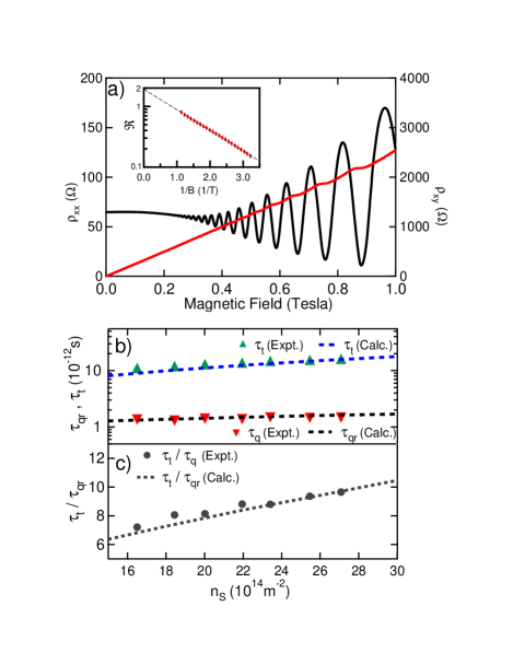
The extracted transport and single particle lifetimes are plotted as solid symbols in Figure 6(b) as a function of the 2D carrier density . As expected, the scattering lifetimes increase with increasing , with the transport lifetime showing a stronger density dependence than the quantum lifetime. The dashed and solid lines show the scattering times calculated for background impurity scattering only. For these calculations the sample is modelled as consisting of two layers, a 160nm thick AlGaAs layer above the 2DEG and a 450m GaAs buffer below it (although has already saturated with a GaAs thickness of 1m). The renormalised quantum lifetime was calculated using the finite thickness scattering potential defined in Eqn. (10). The only fitting parameters were the background impurity density of the AlGaAs and GaAs regions, and . It was only possible to achieve a good fit of the calculated scattering times to the experimental data when and were different, with and giving the best fit. The higher background doping level in the AlGaAs layer is consistent with previous studies showing AlGaAs has a higher background doping level than GaAs Clarke et al. (2006); Laihktman et al. (1990). We note that the quality of the fits and fitting parameters for and were rather insensitive to the thickness of the GaAs region , changing by less than 2% in the range m, whereas was very sensitive to (not shown). This reinforces the need to use the renormalised quantum lifetime.
Fig. 6(b) shows the ratio of the transport to quantum scattering lifetimes for the SISFET sample. This device has no modulation doping, so that scattering is by background impurities only, yet the ratio of scattering lifetimes is of order 10, much larger than the conventional wisdom that for background impurity scattering. This reinforces the rule of thumb introduced earlier, and highlights the need to perform rigorous modelling of experimental scattering times and the ratio in order to determine the limiting scattering mechanism in high quality 2D samples.
V Conclusions
In this paper we have re-analysed the problem of background impurity scattering for 2DEGs in semiconductor heterojunctions. We have shown that current approaches to calculating the quantum lifetime due to background impurities either fail completely, or produce inaccurate results in high quality heterostructures at low electron densities – precisely the area of interest for modern devices. We derived a non-divergent scattering lifetime for finite thickness structures, and have shown that this can be used both with the lowest order perturbation theory and the multiple scattering theory, although only the latter produces physically sensible results. We have found excellent agreement between theoretical calculations and experimental measurements of the scattering times due to background impurities for a GaAs 2DEG in which only background impurity scattering is present. Although our analysis was presented for AlGaAs-GaAs systems, this approach is applicable to generic semiconductor heterostructures.
Acknowledgements.
We thank Fred Green for many useful discussions, and Oleh Klochan for assistance with measurements. This work was funded by the Australian Research Council through the Discovery Projects Scheme (DP0772946); ARH acknowledges an ARC APF grant.References
- Ando et al. (1982) T. Ando, A. B. Fowler, and F. Stern, Reviews of Modern Physics 54, 437 (1982).
- Pfeiffer and West (2003) L. Pfeiffer and K. W. West, Physica E 20, 57 (2003).
- Pfeiffer et al. (1989) L. Pfeiffer, K. W. West, H. L. Störmer, and K. W. Baldwin, Applied Physics Letters 55, 1888 (1989).
- Umansky et al. (1997) V. Umansky, R. de Picciotto, and M. Heiblum, Applied Physics Letters 71, 683 (1997).
- Umansky et al. (in press) V. Umansky, M. Heiblum, Y. Levinson, J. Smet, J. Nübler, and M. Dolev, Journal of Crystal Growth (in press).
- Lilly et al. (1999) M. P. Lilly, K. B. Cooper, J. P. Eisenstein, L. N. Pfeiffer, and K. W. West, Phys. Rev. Lett. 82, 394 (1999).
- Mani (2004) R. G. Mani, Physica E 22, 1 (2004).
- Willett et al. (1987) R. Willett, J. P. Eisenstein, H. L. Störmer, D. C. Tsui, A. C. Gossard, and J. H. English, Phys. Rev. Lett. 59, 1776 (1987).
- Sarma et al. (2005) S. Das Sarma, M. Freedman, and C. Nayak, Physical Review Letters 94, 166802 (pages 4) (2005).
- Hwang and Sarma (2008) E. H. Hwang and S. Das Sarma, Physical Review B 77, 235437 (pages 6) (2008).
- Gottinger et al. (1988) R. Gottinger, A. Gold, G. Abstreiter, G. Weimann, and W. Schlapp, Europhysics Letters 6, 183 (1988).
- Bockelmann et al. (1990) U. Bockelmann, G. Abstreiter, G. Weimann, and W. Schlapp, Physical Review B 41, 7864 (1990).
- Dingle et al. (1978) R. Dingle, H. L. Störmer, A. C. Gossard, and W. Wiegmann, Appl. Phys. Lett. 33, 665 (1978).
- Störmer et al. (1981) H. L. Störmer, A. Pinczuk, A. C. Gossard, and W. Wiegmann, Applied Physics Letters 38, 691 (1981).
- Kane et al. (1993) B. E. Kane, L. N. Pfeiffer, K. W. West, and C. K. Harnett, Applied Physics Letters 63, 2132 (1993).
- Harrang et al. (1985) J. P. Harrang, R. J. Higgins, R. K. Goodall, P. R. Jay, M. Laviron, and P. Delescluse, Physical Review B 32, 8126 (1985).
- Sarma and Stern (1985) S. Das Sarma and F. Stern, Physical Review B (Rapid Communications) 32, 8442 (1985).
- Coleridge et al. (1989) P. T. Coleridge, R. Stoner, and R. Fletcher, Physical Review B 39, 1120 (1989).
- Kearney et al. (2000) M. J. Kearney, A. I. Horrell, and V. M. Dwyer, Semiconductor Science Technology 15, 24 (2000).
- Gold (1988) A. Gold, Physical Review B 38, 10798 (1988).
- Gold and Götze (1986) A. Gold and W. Götze, Physical Review B 33, 2495 (1986).
- Gold and Götze (1981) A. Gold and W. Götze, J. Phys. C: Solid State Phys. 14, 4049 (1981).
- Davies (2000) J. H. Davies, The Physics of Low-Dimensional Semiconductors, An Introduction (Cambridge University Press, 2000).
- Solomon et al. (1984) P. M. Solomon, C. M. Knoedler, and S. L. Wright, IEEE Electron Device Letters 5, 379 (1984).
- Footnote 1 (2009) A thin GaAs capping layer is often present in modulation doped structures, to prevent oxidation of the AlGaAs, but this can be treated as part of the AlGaAs layer for the purposes of background impurity scattering.
- Fang and Howard (1966) F. F. Fang and W. E. Howard, Physical Review Letters 16, 797 (1966).
- Footnote 2 (2009) The form factors given in Eqn. (5) differ from those given by Gold in Ref. Gold (1989) by a factor of 1/2. This factor of 1/2 comes from the integration of Eqn. (6), and can either be accounted for in the form factors of Eqn. (5) (as Gold does) or in the of Eqn. (7) (as we do).
- Gold (1989) A. Gold, Applied Physical Letters 54, 2100 (1989).
- Gold (1990) A. Gold, Physical Review B 41, 8537 (1990).
- Gold (1985) A. Gold, Physical Review Letters 54, 1079 (1985).
- Klauder (1961) J. R. Klauder, Annals of Physics 14, 43 (1961).
- MacLeod et al. (2007) S. J. MacLeod, T. P. Martin, A. P. Micolich, and A. R. Hamilton (SPIE, 2007), vol. 6800, p. 68001L.
- Zhu et al. (2003) J. Zhu, H. L. Störmer, L. N. Pfeiffer, K. W. Baldwin, and K. W. West, Phys. Rev. Lett. 90, 056805 (2003).
- Coleridge (1991) P. T. Coleridge, Phys. Rev. B 44, 3793 (1991).
- Clarke et al. (2006) W. R. Clarke, A. P. Micolich, A. R. Hamilton, M. Y. Simmons, K. Muraki, and Y. Hirayama, Journal of Applied Physics 99, 023707 (2006).
- Laihktman et al. (1990) B. Laihktman, M. Heiblum, and U. Meirav, Applied Physics Letters 57, 1550 (1990).