Large contrast enhancement of graphene monolayers by angle detection
Abstract
Exfoliated graphene monolayers are identified by optical inspection. In order to improve the monolayer detection, we investigate the angle dependence of the optical contrast of graphene on a 90nm SiO2/Si substrate. We observe a significant enhancement of the visibility of graphene by changing the polarization and the angle of optical incidence. This method can be used to detect graphene on new substrate designs such as GaAs/AlAs based materials, which have a much cleaner surface.
pacs:
78.67.-n, 68.65.AcSince its discovery in 2004 novo04 , graphene, a monolayer of carbon atoms packed into a honeycomb lattice led to an explosion of work. The high electronic mobility of intrinsic graphene makes it a very attractive candidate for electronicsgeim07 . Indeed, graphene on SiO2 substrates have shown very high mobilities tan07 at room temperature, but when the devices are cooled, mobilities do not improve significantly chen08 , which is in stark contrast to the highest mobilities in GaAs/AlGaAs pfeiffer03 . At low temperatures, the mobility is limited by scattering due to charged impurities chen08 ; hwang07 and the presence of ripples in graphene on SiO2 ishig07 ; chen08-2 ; chen09 .
Graphene monolayers can be obtained by exfoliation or by epitaxy. However, in graphene epitaxy the quantum Hall effect is not clearly seen because of the coupling to the substrate didier08 , which leads to a decreasing mobility as a function of magnetic field. In contrast, uncoupled single layers of graphene can be deposited via micromechanical cleavage of graphite flakes novo05 . Since the active electronic region in graphene is only one atom away from the substrate, the quality of the substrate will substantially influence the electronic properties as demonstrated by the increase of mobility for suspended graphene bol08 . However, it is very difficult to make advanced devices out of suspended materials. This brings us to consider the possibility to deposit graphene on different substrates, while still providing for a good visibility.
Graphene layers can be localized on oxidized Si wafers through changes of the reflection at optical wavelengths. Optimal thicknesses of the oxide layer are found to be 90 and 300 nm and lead to an optical contrast of about 15% for a graphene monolayer blake07 ; aberg07 ; rodd07 ; chang07 ; jung07 . Adding a resist layer can enhance the contrast gteo08 but requires the deposition of a very uniform resist before localizing the interesting flakes. Here we discuss an alternate route to increase the contrast of a graphene monolayer. The main idea is to increase the contrast by polarizing and directing the incoming light at various angles.
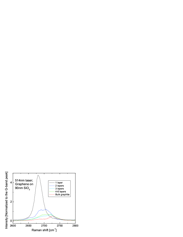
Graphene is deposited using natural graphite from Asbury Carbon via mechanical exfoliation. In order to identify single layered graphene flakes, we performed calibration measurements using Raman spectroscopy as seen in Figure 1. This technique can be used as a reference for optical contrast coding gupta06 and maps the number of layers to an optical contrast value. Once single layered graphene flakes were identified we measured the angle dependence of the contrast for different colors. We used a white light source and recorded the signal at different wavelengths.
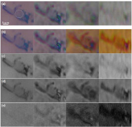
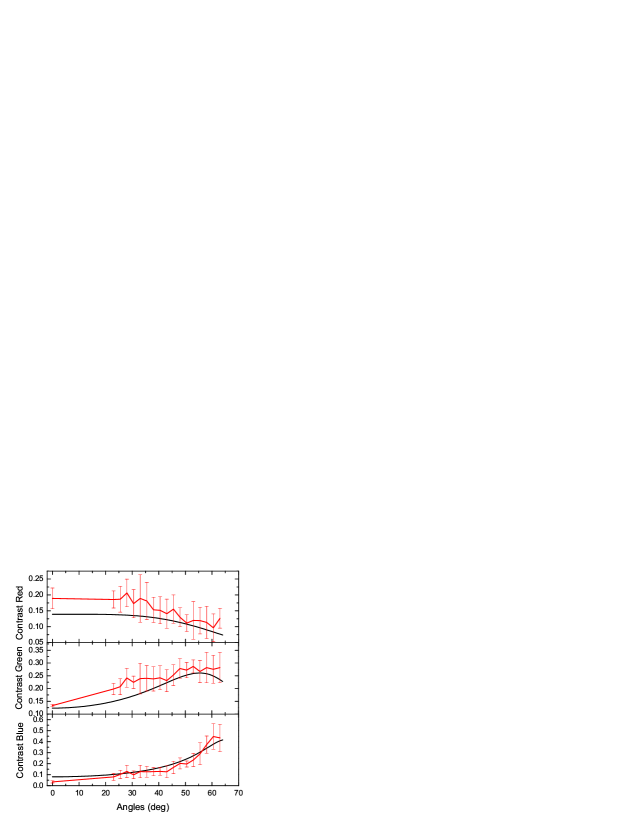
The first column of Figure 2 is a typical image of a graphene mono-layer at normal incidence. By increasing this angle, corresponding to images from left to right, the colors of the SiO2 and graphene change. Figure 2(a) is obtained with TM (Transverse Magnetic) polarization and as the angle increases, a decrease in contrast of graphene is observed for all wavelengths. With TE (Transverse Electric) polarization, Figure 2(b) shows a change in color with increased angle. In order to analyze the contrast, we selected a red, green and blue wavelength respectively (Figure 2(c)(d)(e)). A decrease of contrast is seen in the red as the angle increases, while the contrast for green and blue increases. We can understand these changes in terms of the following simple multilayered optical model.
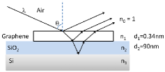
We consider a SiO2/Si substrate with an oxide thickness of 90nm (taken from the measured value of 902nm), while the thickness of a graphene monolayer is set to 0.34nm. We then consider an incoming light beam of wavelength (the external light source), which hits a trilayer structure (graphene/SiO2/Si) and passes through a series of reflections and transmissions as seen in Figure 3. The Si layer is assumed to be semi-infinite. The index of refraction of SiO2 (n2) and Si (n3) are wavelength dependent and their values are given in Ref. handb91, and henrie04, . The index of refraction of graphene is assumed to be the same as that of bulk graphite (n1 2.6 + 1.3i) handb91 .
 |
 |
The results are obtained by considering a system of 3 layers (Figure 3) in which each layer j can be represented by a transfer matrix. For a TM polarization, the magnetic field component Hz is parallel to the layers and the electrical component Ey is at the incident angle . The general form of the transfer matrix for a layer j can be written as hilke08 ; chilwell84 :
| (1) |
The relation of the field components for a wavelength can be expressed as the product of transfer matrices (M = Mj) with the reflectance given by
| (2) |
where Mkl are the matrix elements of M. The matrix Mj in Equation 1 depends on the index of refraction () and width () of the corresponding layer, with , , and the vacuum impedance . For the TE polarization, the expressions have to be substituted by , , and . Once the reflectance is computed, the contrast is given by , where is the reflectance without graphene and the reflectance in the presence of graphene.
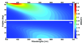
While several groups have computed the contrast at normal incidence blake07 ; jung07 ; gteo08 , we show here the results as a function of incident angle for different polarizations. Figure 3 shows the evolution of the contrast as function of angle in the visible spectrum for two polarizations. While no contrast enhancement is obtained for TM polarizations, TE polarizations show a significant enhancement in the blue wavelengths. We compare the calculated contrast with the data for different wavelengths in Figure 4. The data follows the calculated one within the error bars obtained from the standard deviation of several different data sets. Clearly, the blue and green wavelengths show a significant increase in contrast as a function of angle, reaching even 40% for blue.
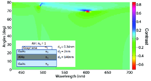
Based on our understanding of the contrast on SiO2, we now turn to the possibility of enhancing the contrast of graphene on other substrates, which would offer a smoother and cleaner electrical surface than SiO2. Here, we consider an optimal GaAs/AlAs/GaAs heterostructure which can be grown by molecular beam epitaxy. It was previously reported in Ref. gteo08, that the optimal contrast for a homostructure of GaAs is -0.0059. Here, we propose a 4-layer Fabry-Pérot structure suitable to increase the contrast for the detection of a single layer graphene as shown in the inset of Figure 5. For this structure, the intensity of the reflected waves is calculated by considering an additional layer, leading to an extra transfer matrix in Equation 1. The first GaAs layer is described by a thickness of d2 and its refractive index is wavelength dependent handb91 . For simplicity, the thickness d2 is fixed at 2nm since the smallest layer of GaAs improves the overall contrast of graphene. It is important to have GaAs as a cap layer since it is a much cleaner surface than AlAs, which oxidizes much more. Next, the thickness of the AlAs layer () was varied and found to be optimal at 140nm. In Figure 5 we show the contrast as a function of incident angle. At normal incidence, a contrast of 2% was obtained, which improves the contrast by almost a factor of 4 compared to a monostructure of GaAs. As the angle increases to 65 degrees, the expected contrast is approximately 14%. This contrast is identical to graphene on SiO2 at normal incidence and should allow the identification of graphene monolayers on GaAs. Interestingly, the contrast for GaAs is only enhanced for a TM polarization as opposed to a TE polarization in the SiO2 case.
In summary, we found a simple way to increase the contrast of a single layer of graphene on SiO2 by simply tilting the sample and the light source. This method can then be applied to other substrates, such as GaAs/AlAs heterostructures, which have much cleaner surfaces in order to substantially increase the mobilities.
We would like to acknowledge helpful discussions with T. Szkopek, and support from NSERC, FQRNT, and RQMP.
References
- (1) K. S. Novoselov, A. K. Geim, S. V. Morozov, D. Jiang, Y. Zhang, S. V. Dubonos, I. V. Grigorieva, and A. A. Firsov, Science 306, 666 (2004).
- (2) A. K. Geim and K. S. Novoselov, Nat. Mater. 6, 183 (2007).
- (3) Y.-W. Tan, Y. Zhang, K. Bolotin, Y. Zhao, S. Adam, E. H. Hwang, S. Das Sarma, H. L. Stormer, and P. Kim, Phys. Rev. Lett. 99, 246803 (2007).
- (4) J.-H. Chen, C. Jang, S. Adam, M. S. Fuhrer, E. D. Williams, and M. Ishigami, Nat. Phys. 4, 377 (2008).
- (5) L. Pfeiffer and K. W. West, Physica E 20, 57-64 (2003).
- (6) E. H. Hwang, S. Adam, and S. Das Sarma, Phys. Rev. Lett. 98, 186806 (2007) .
- (7) M. Ishigami, J-H. Chen, W. G. Cullen, M. S. Fuhrer, and E. D. Williams, Nano Lett. 7, 6 (2007).
- (8) J.-H. Chen, C. Jang, S. Xiao, M. Ishigami, and M. S. Fuhrer, Nature Nanotech. 3, 206 (2008).
- (9) J.-H. Chen, C. Jang, M. Ishigami, S. Xiao, E. D. Williams, and M. S. Fuhrer, Solid State Communications 149, 1080 (2009).
- (10) P. Darancet, N. Wipf, C. Berger, W. A. de Heer, and D. Mayou, Phys. Rev. Lett. 101, 116806 (2008).
- (11) K. S. Novoselov, D. Jiang, F. Schedin, T. J. Booth, V. V. Khotkevich, S. V. Morozov, and A. K. Geim, Proc. Natl. Acad. Sci. U.S.A. 102, 10451 (2005).
- (12) K. I. Bolotin K. J. Sikes, Z. Jiang, M. Kilma, G. Fudenberg, J. Hone, P. Kim, and H. L. Stormer, Solid State Communications 146, 351-355 (2008).
- (13) P. Blake, K. S. Novoselov, A. H. Castro Neto, D. Jiang, R. Yang, T. J. Booth, A. K. Geim, and E. W. Hill, Appl. Phys. Lett. 91, 063124 (2007).
- (14) D. S. L. Abergel, A. Russell, and V. I. Fal’ko, Appl. Phys. Lett. 91, 063125 (2007).
- (15) S. Roddaro, P. Pingue, V. Piazza, V. Pellegrini, and F. Beltram, Nano Lett. 7, 2707 (2007).
- (16) K. Chang, J. T. Liu, J. B. Xia, and N. Dai, Appl. Phys. Lett. 91, 181906 (2007).
- (17) I. Jung, M. Pelton, R. Piner, A. D. Dikin, S. Stankovich, S. Watcharotone, M. Hausner, and R. S. Ruoff, Nano Lett. 7, 12 (2007).
- (18) G. Teo, H. Wang, Y. Wu, Z. Guo, J. Zhang, Z. Ni, and Z. Shen, J. Appl. Phys. 103, 12 (2008).
- (19) A. Gupta, G. Chen, P. Joshi, S. Tadigadapa, and P. C. Eklund, Nano Lett. 6, 12 (2006).
- (20) Handbook of Optical Constants of Solids, edited by E. D. Palik (Academic, New York, 1991), vol. 2.
- (21) J. Henrie, S. Kellis, S. Schultz, and A. Hawkins, Opt. Express 12, 1464 (2004).
- (22) M. Hilke, e-print arXiv:cond-mat/0812.3450
- (23) J. Chiwell and I. Hodgkinson, J. Opt. Soc. Am. A 1, 742-753 (1984).