Spin Filtering in a Nonuniform Quantum Wire with Rashba Spin-Orbit Interaction
Abstract
We investigate theoretically the spin-polarized electron transport for a wide-narrow-wide (WNW) quantum wire under the modulation of Rashba spin-orbit interaction (SOI). The influence of both the structure of the quantum wire and the interference between different pairs of subbands on the spin-polarized electron transport is taken into account simultaneously via the spin-resolved lattice Green function method. It is found that a very large vertical spin-polarized current can be generated by the SOI-induced effective magnetic field at the structure-induced Fano resonance even in the presence of strong disorder. Furthermore, the magnitude of the spin polarization can be tuned by both the Rashba SOI strength and structural parameters. Our results may provide an effective way to design a spin filter device without containing any magnetic materials or applying a magnetic field.
pacs:
73.63.Nm, 71.70.Ej, 72.25.DcI INTRODUCTION
Spintronics, aiming to use electron spin instead of charge degree of freedom to store and communicate information, has drawn considerable attention in the past decades.1 In this field, the Rashba SOI2,3 plays an important role since it has been expected to be used to manipulate spin states and its strength can be tuned by external gate voltage conveniently.4-6
It is well known that one indispensable requirement of spintronics applications is to be capable of generating a spin-polarized current. Various schemes such as spin injection,7 spin hall effect8-9 as well as spin filtering10-21 have been proposed to satisfy this goal. Among these schemes, the spin filtering, which generates a tunable spin-polarized current out of unpolarized sources, is the most promising candidate. Recently, a interesting SOI-induced Fano resonance is found in quantum wire with local Rashba SOC. This effect originates from the SOI-induced bound state couples to conductance one through Rashba intersubband mixing, giving rise to pronounced dips in the linear conductance.22 These dips at the SOI-induced Fano resonances have the typical Fano line shape. Apart from the SOI-induced Fano resonance, there is another type of Fano resonance, that is, structure-induced Fano resonance, which results from the Fano-type interference between the continuous subband states and a bound state formed in the system. A transverse spin-polarized current can be created at these SOI-induced and structure-induced Fano resonances from a unpolarized injection has been predicted by Zhai and Xu.17 However, the maximum value of this transverse spin polarization is not more than 0.5 because only at least two propagating modes involved in the transport can the spin polarized current be created. Thus it is not known whether a large spin-polarized current can be generated at other directions at the structure-induced Fano resonance from a spin-unpolarized injection and whether the magnitude of the spin polarization can be enhanced by designing an appropriate structure of the considered system.
In the present work, we calculate the spin polarized electron conductance for a WNW wire with Rashba SOI by the spin-resolved lattice Green function method. It is shown that a very large vertical spin-polarized current can be generated in this system because of the mirror asymmetry with respect to the longitudinal axis and the structure-induced Fano resonance. The degree of the generated vertical spin-polarized current can be tuned by both the strength of Rashba SOI and the structural parameters. The more important result is that this vertical spin-polarized current with strong a robustness against disorder. The organization of this paper is as follows. In section II, the theoretical model and the calculation method are presented. In section III, the numerical results are illustrated and discussed. A conclusion is given in section IV.
II MODEL AND ANALYSIS
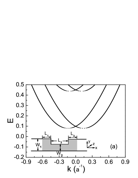
The investigated system is depicted in the inset of Fig. 1(a) schematically, where a two-dimensional electron gas (2DEG) in the plane is restricted to a WNW quantum wire by a hard-wall transverse confining potential . The 2DEG is confined in a asymmetric quantum well, where the SOI is assumed to arise dominantly from the Rashba mechanism. The narrow part of the quantum wire has a width and a length . The wide parts of the quantum wire have the same width but different lengths and , connected to two ideal semi-infinite leads with the same width at each end. Since we are only concerned with spin-unpolarized injection, the two connecting leads are nonmagnetic and have a vanishing SOI. After discreting procedure, a type of tight-binding Hamiltonian including the Rashba SOI on a square lattice is obtained,
| (1) |
where is the creation (annihilation) operator of electron at site with spin . The on-site energy is with the hopping energy , where and are the effective mass of electron and lattice constant, respectively. The Rashba SOI strength is and is Pauli matrix.
In the ballistic transport, the spin-resolved conductance is given by Landauer-Bttiker23 formalism with the help of the nonequilibrium Green function formalism.24 The two-terminal spin-resolved conductance is given by , where , is the self-energy from the left (right) lead, is the retarded (advanced) Green function of the whole system, and the lead effect is incorporated into the self-energy of Green function . The trace is over the spatial degrees of freedom. The Green function above is computed by the well-known recursive Green function method.25,26 The local density of electron states (LDOS) is described as27 , where is the emitting energy of electrons. In our following calculation, the axis is chosen as the spin-quantized axis, all the energy is normalized by the hoping energy , and the structural parameters of the wire are fixed at , , and except the variables in Fig. (5). The charge conductance and the vertical spin polarization are defined as and , respectively.
III RESULTS AND DISCUSSION
The energy-subband dispersions of the narrow and wide part of the quantum wire are plotted in Fig. 1(a) and Fig. 1(b), respectively. The Rashba SOI strength . It is shown that a linearly Rashba spin-split subband is obtained in Fig. 1(a). However, the spin-subband dispersion in Fig. 1(b) deviates considerably from the typical linearly Rashba splitting. This is because the SOI strength in the narrow region lies in the weak-coupling regime while it lies in the strong-coupling regime in the wide regions due to their different widths.8
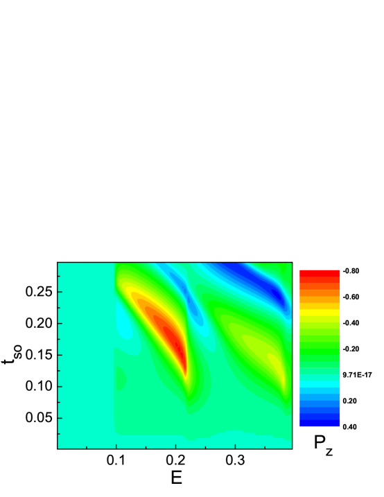
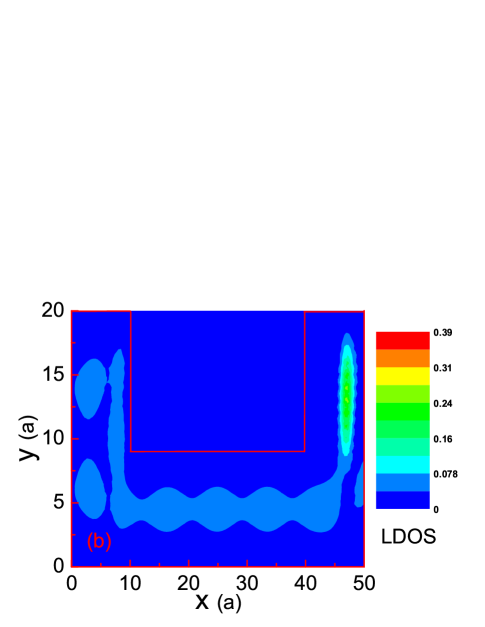
Figure 2 shows the calculated spin polarization as a function of the emitting energy and the strength of Rashba SOI . When the emitting energy , a vertical spin-polarized current can be obtained in the right lead since the injected current from the left lead is unpolarized. This vertical spin-polarized current arising from the Rashba intermixing between different pairs of transverse modes and the mirror symmetry with respect to the y-axis is broken.11 According to the left-right and time-reversal symmetries, the relation is obtained while the relation cannot be guaranteed, which can be proved by checking the numeric calculation. Surprisingly, there appears a very large vertical spin-polarized current when the emitting energy be about to 0.2. In order to clarify this effect, the charge conductance as a function of the emitting energy at is illustrated in Fig. 3(a) and the corresponding spin polarization is shown in the inset of Fig. 3(a). When , the conductance is zero since all the subbands of the narrow region are evanescent modes. When , only the lowest one pair of subbands of the wide and narrow regions are propagating modes, so there is no spin polarized current.28 Moreover, when , the lowest two pairs of subbands of the wide regions become propagating modes and the subband intermixing induced by the Rashba SOI arises, resulting in the nonzero spin polarized current. However, there is still a pair of propagating modes in the narrow region, which determines the charge conductance of the whole system. Consequently, the vertical spin polarization may be larger than 0.5. It is worth to note that a ‘valley’ like structure appears in the charge conductance when the emitting energy just near the threshold of the third pair of propagating modes in the wide regions, i.e., . This effect can be attributed to the constriction in the narrow part, leading to the formation of a bound state in the right wide region. And the bound state couples to the conductance ones through Rashba intersubband mixing, giving rise to a structure-induced Fano resonance. Amazingly, a very large vertical spin polarization can be achieved in the right lead at this Fano resonance. Fig. 3(b) displays the LDOS at and . It is obvious that electrons are confined in the top of the right wide region under the present parameters. Of course, there are other structure-induced or SOI-induced Fano resonances near the thresholds of the second and the fourth pair of propagating modes in the wide region, i.e., and , but the spin polarization at this two points is much smaller than that at .
The spin polarization as a function of the strength of Rashba SOI at is shown in Fig. 4. The spin polarization becomes larger with the increasing of the strength of Rashba SOI and reaches its maximum value as , which consists with the maximum value of the inset in Fig. 3(a). However, the spin polarization becomes smaller as the Rashba SOI strength further increases. It indicates that the spin polarization at the structure-induced Fano resonance can be manipulated by variation of the Rashba SOI strength. Apart from the strength of Rashba SOI, the structural parameters of the investigated system can also be used to control the magnitude of the spin polarization. Figure 5(a) shows the calculated spin polarization as a function of the width of the narrow region when and . The spin polarization becomes larger as the width of the narrow region increases and reaches its maximum value at . In addition, there appears a sharp step as the width of the narrow region reaches . Furthermore, the spin polarization reaches zero when , namely, the spin-polarized current disappears, which results from the structural and time-reversal symmetries. According to Fig. 3(b), the bound state exists in the top of the right wide region. Therefore, the spin polarization is only related to the length of this region while has nothing to do with the length of the left wide region. The calculated spin polarization as a function of the length of the right wide region is plotted in Fig. 5(b). The emitting energy and SOI strength are the same as that in Fig. 5(a). The most interesting features are that a dip emerges in the spin polarization when and the spin polarization oscillates around zero when .
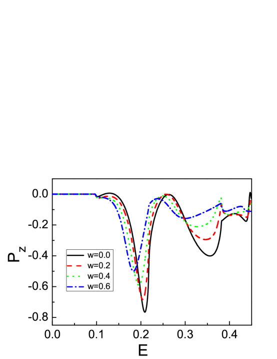
The above calculation assumes perfectly clean system, where there is no elastic or inelastic scattering. However, in a realistic system, there will be many impurities in the sample. Consequently, the effect of disorder should be considered in practical application. The disorder could be incorporated by the fluctuation of the on-site energies, which distributes randomly within the range width [ with ]. Figure 6 shows the calculated spin polarization as a function of the emitting energy for (weak and strong) different disorders . The SOI strength is set as . It can be seen that the spin polarization at the structure-induced Fano-resonances decreases with the increasing of disorder. However, the spin polarization at the second Fano-resonance almost equals to even when , which implies that the spin-polarized current can still survive in the presence of strong disorder.
IV CONCLUSION
In conclusion, we have studied the spin-polarized electron transport through a WNW quantum wire under the modulation of Rashba SOI. The presence of the SOI and the asymmetry in the longitudinal direction leading to a vertical spin-polarized current in the right lead. In particular, we have shown that a very large vertical spin polarization can be obtained at the structure-induced resonance and its degree can be controlled by both the strength of Rashba SOI and the structural parameters even in the presence of strong disorder. This effect may provide an efficient method to design a spin filter without applying an external magnetic field and without attaching ferromagnetic contacts.
ACKNOWLEDGMENT
This work was supported by the National Natural Science Foundation of China under Grant No. 10774112.
References
- (1) 1 I. Zutic, J. Fabian, and S. D. Sarma, Rev. Mod. Phys. 76 323 (2004).
- (2) 2 G. Lommer, F. Malcher, and U. Rssler, Phys. Rev. Lett. 60 728 (1988).
- (3) 3 E. A. Andradae Silva, G. C. L. Rocca, and F. Bassani, Phys. Rev. B 50 8523 (1994).
- (4) 4 J. Nitta, T. Akazaki, H. Takayanagi, and T. Enoki, Phys. Rev. Lett. 78 1335 (2002).
- (5) 5 D. Grundler, Phys. Rev. Lett. 84 6074 (2000).
- (6) 6 T. Koga, J. Nitta, T. Akazaki, and H. Takayanagi, Phys. Rev. Lett. 89 046801 (2002).
- (7) 7 A. T. Hanbicki, M. J. vant ErveO, R. Magno, G. Kioseoglou, C. H. Li, and B. T. Jonker, Appl. Phys. Lett. 82 4092 (2003).
- (8) 8 S. C. Zhang, Phys. Rev. Lett. 85 393 (2000).
- (9) 9 J. Sinova, D. Culcer, Q. Niu, N. A. Sinitsyn, T. Jungwirth, and H. MacDonald, Phys. Rev. Lett. 92 126603 (2004).
- (10) 10 A. A. Kiselev and K. W. Kim, J. Appl. Phys. 94 4001 (2003).
- (11) 11 Q. W. Shi, J. Zhou, and M. W. Wu, Appl. Phys. Lett. 85 2547 (2004).
- (12) 12 Q. F. Sun and X. C. Xie, Phys. Rev. B 71 155321 (2005).
- (13) 13 J. Ohe, M. Yamamoto, T. Ohtsuki, and J. Nitta, Phys. Rev. B 72 041308(R) (2005).
- (14) 14 M. Lee and C. Bruder, Phys. Rev. B 73 085315 (2006).
- (15) 15 H. X. Wang, S. J. Xiong, and S. N. Evangelou, Phys. Lett. A 356 376 (2006).
- (16) 16 Z. Y. Zhang, J. Phys: Condens. Matter 19 016209 (2006).
- (17) 17 F. Zhai and H. Q. Xu, Phys. Rev. B 76 035306 (2007).
- (18) 18 S. J. Gong and Z. Q. Yang J. Appl. Phys. 102 033706 (2007).
- (19) 19 G. H. Liu and G. H. Zhou, J. Appl. Phys. 10 063704 (2007).
- (20) 20 S. Bellucci and P. Onorato Phys. Rev. B 77 075303 (2008).
- (21) 21 A. Aharony, O. Entin-Wohlman, Y. Tokura, and S. Katsumoto, Phys. Rev. B 78 125328 (2008).
- (22) 22 D. Snchez and L. Serra, Phys. Rev. B 74 153313 (2006).
- (23) 23 M. Bttiker, Phys. Rev. Lett. 57 1761 (1986).
- (24) 24 T. P. Pareek and P. Bruno, Phys. Rev. B 63 165424-1 (2001); L. W. Molenkamp, G. Schmidt, and G. E. W. Bauer, Phys. Rev. B 62 4790 (2000).
- (25) 25 P. A. Lee and D. S. Fisher, Phys. Rev. Lett. 47 882 (1981).
- (26) 26 T. Ando, Phys. Rev. B 44 8017 (1991); M. J. Mclennan, Y. Lee, and S. Datta, Phys. Rev. B 43 13846 (1991); H. U. Baranger, D. P. Divincenzo, R. A. Jalaber, and A. D. Stone, Phys. Rev. B 44 10637 (1991).
- (27) 27 S. Datta, Electronic Transport in Mesoscopic Systems (Cambridge University Press, New York, 1997).
- (28) 28 F. Zhai and H. Q. Xu, Phys. Rev. Lett. 94 246601 (2005).
- (29)