Terahertz response of carbon nanotube transistors
Abstract
We present an approach for time-dependent quantum transport based on a self-consistent non-equilibrium Green function formalism. The technique is applied to a ballistic carbon nanotube transistor in the presence of a time harmonic signal at the gate. In the ON state the dynamic conductance exhibits plasmonic resonant peaks at terahertz frequencies. These vanish in the OFF state, and the dynamic conductance displays smooth oscillations, a signature of single particle quantum effects. We show that the nanotube kinetic inductance plays an essential role in the high-frequency behavior.
pacs:
72.10.Bg, 72.30.+q, 73.22.Lp, 73.63.Fg, 85.35.KtNanoelectronic devices using nanotubes and nanowires as their active elements have been extensively studied for their DC properties CNTDC . However, their high-frequency AC characteristics have received little attention despite the obvious importance for many applications and the breadth of intriguing scientific questions. Experimental work in carbon nanotube (NT) and graphene field-effect transistors (FETs) have indicated little performance degradation up to GHz frequencies ExpRFCNT ; and recently, time-domain measurements in the terahertz (THz) regime have been used to distinguish between plasmon and single-particle excitations at low temperatures in NTs McEuenNNT08 .
This progress in measuring the high-frequency properties of NTs poses challenging questions for theory and modeling, in particular on how to describe the carrier quantum dynamics under non-equilibrium conditions in realistic device geometries, along with the self-consistent feedback between the time-dependent charge and potential, which is essential to capture the plasmonic excitations of the system BohmPR49 . In addition, one open question is whether single-particle and plasmon excitations can be distinguished in low-dimensional systems.
In this paper, we address these questions by proposing a formalism for AC quantum transport making use of non-equilibrium Green functions (NEGF) Haug1998 , and apply it to determine the high-frequency properties of NTFETs. We find that the dynamic conductance exhibits both smooth oscillations and divergent features in the THz regime, indicating the coexistence of single-particle and collective excitations (plasmons). In addition, by calculating the dynamic capacitance, we show that the nanotube kinetic inductance plays a central role in determining the high-frequency behavior, in contrast to conventional FETs.
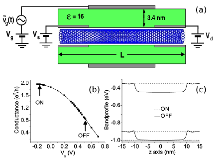
We begin by describing our theoretical approach using the example of a NTFET as illustrated in Fig. 1a. (NTs are ideal to study ballistic high-frequency transport due to the large electron mean-free path for acoustic phonon scattering, even at room temperature PurewalPRL07 .) The system is divided into a device region which is connected to two semi-infinite leads consisting of NTs embedded in source and drain metals. The salient feature is the presence of a time-dependent potential at the gate terminal, , and we are interested in the dynamic source-drain conductance . This is a much different problem than the one treated previously mostly within a non-self-consistent approach where either a time-dependent potential was applied to the source and drain electrodes TheoAC1 or simplified one- or two-level systems were used TheoAC2 .
In the absence of , the system is described by the retarded/advanced () Green function
| (1) |
where is a positive infinitesimal constant. is the time-independent Hamiltonian of the device region while couples the device region and the semi-infinite leads; is the time-independent, spatially-dependent, self-consistent DC electrostatic potential. This Green function forms the basis for calculations of the DC transport properties of nanosystems. In the presence of , a time- and spatially-dependent electrostatic potential is generated in the device region. must be determined based on the complex environment of the nanosystem, and must satisfy self-consistency between charge and electrostatic potential, as will be discussed further below. Because of the presence of this time-dependent potential, the relevant Green function is the two-time function
| (2) |
We obtain the frequency-dependent particle current at terminal from the time derivative of the number operator as
| (3) |
where . The AC Green functions appearing in Eq.(3) are obtained from Dyson’s equation , whereas the non-equilibrium particle density reads following the standard procedure Haug1998 . refers to the particle distribution of the unperturbed system with , and the Fermi function of terminal .
The above set of equations provides an approach to calculate the frequency-dependent quantum transport in the NEGF technique. These equations need to be augmented to include the coupling of the quantum transport equations with the electrostatics, as embodied by Poisson’s equation:
| (4) |
(At the frequencies of interest here, the time dependence of the full Maxwell equations can be neglected.) This contribution is especially important to capture the complex environments of nanoelectronic devices, and plasmonic effects. Poisson’s equation is complemented by appropriate boundary conditions at the terminals; in particular at the gate terminal, a time-dependent potential is applied and serves as the external perturbation that generates .
A closed set of equations can be obtained by expressing the charge density from the Green function:
| (5) |
Thus, the set of Eqs. provides an approach to calculate self-consistently the frequency-dependent current in the presence of a frequency-dependent external gate potential. We note that our approach does not rely on approximations to the wide- or narrow-band limits, but treats the spectral properties of the contacts explicitly.
To proceed further, we consider to be a small perturbation and expand the above equations to linear order in . The Green function of the perturbed system can be obtained from Dyson’s equation as , while (a superscript indicates a function evaluated at ). In practice, one is often interested in the small-signal response of the two-terminal conductance . To obtain an expression for , we consider a time-harmonic gate potential which generates an electrostatic potential on the NT. Expanding to lowest order in and we obtain for the particle conductance
| (6) | |||||
where for a general function .
In general, the particle conductance does not obey fundamental sum rules for current conservation and gauge invariance, since the displacement current has been omitted. To include it, we adopt the scheme of Wang et.al. GuoPRL99 , where the final conductance is given by , and derive for the frequency-dependent displacement conductance
| (7) | |||||
Note that measures the change in the conductance relative to the value at the DC operation point.
We now apply the AC theory outlined above to calculate the zero-bias AC conductance at K for the NTFET of Fig. 1a. The first step is to obtain the DC properties of the NTFET; details of the numerical procedures are given in Ref. LeonNT06 . The (17,0) NT of radius nm is modeled using a -tight-binding model with an overlap energy of eV, giving a bandgap of eV. The Fermi levels of the source and drain metals are set 1 eV below the NT midgap before self-consistency, which gives a p-type ohmic contact after self-consistency. Fig. 1b shows the DC transfer characteristics of the NTFET with a channel length nm, which consist of an ON-state where the bands are essentially flat, and an OFF-state where a gate-controlled barrier blocks the hole current (Fig. 1c).
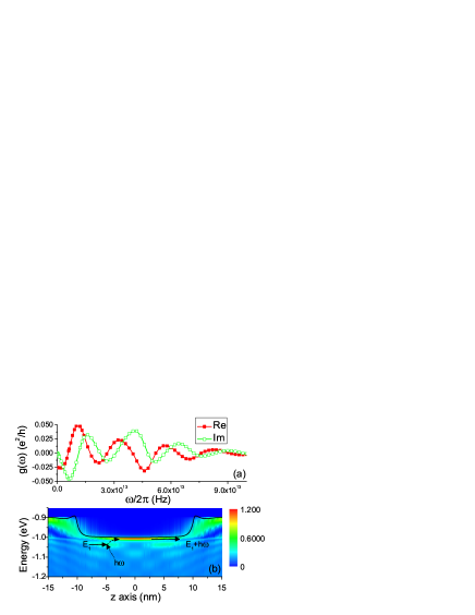
To explore the AC behavior of the NTFET, we first choose a DC operating point, either in the ON or OFF state as marked by arrows in Fig. 1b, and apply an AC gate signal perturbation of frequency and magnitude meV. Figure 2a shows the real and imaginary parts of the AC conductance in the OFF state which displays smooth oscillations as a function of frequency. ( is negative because the AC perturbation reduces to a positive DC voltage perturbation . According to the DC transfer characteristics of Fig. 1b an increase in DC gate bias leads to a reduced conductance.) Surprisingly, for finite frequencies the AC conductance can take values larger than the DC conductance. The origin of this behavior and of the smooth oscillations can be understood from the spatially and energy dependent density of states (DOS) in the OFF state shown in Fig. 2b. At a given position along the NT the DOS shows oscillations in energy with a characteristic frequency of about THz. The maxima in arise from the photoexcitation of carriers between maxima of the DOS while the minima in arise from the excitation between maxima and minima of the DOS. Thus, in the OFF state, smooth conductance oscillations are a signature of the single-particle excitation spectrum. The oscillatory character of is preserved when the self-consistent feedback between charge and potential is disabled (not shown), confirming this nature of transport.
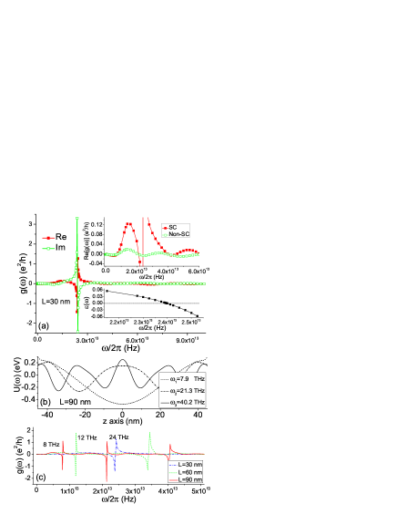
Figure 3a displays the real and imaginary parts of the dynamic conductance for the same NTFET in the ON-state, which is also slightly negative at for the same reason as in the OFF-state. We observe that the response for frequencies less than about THz is constant, in agreement with the experiments in Ref. ExpRFCNT . For larger frequencies we observe that the conductance exhibits a pronounced divergent response at THz with an underlying oscillatory behavior. Near the divergence, the self-consistent potential along the NT reveals large amplitude oscillations, which change phase as the divergence is crossed. These large amplitude oscillations are shown for a device with nm channel length in Fig. 3b, including the higher-order modes. The presence of these oscillatory modes suggests that plasmons are responsible for the divergent behavior. In order to ascertain that the response calculated in the ON-state can be attributed to collective rather than single particle excitations, we compare in Fig. 3a (top inset) the self-consistent (SC) response with the non-self-consistent solution obtained from the first iteration. The divergence in the conductance disappears entirely while the smooth oscillations persist. Thus, the self-consistency between the charge and potential is essential to observe the divergence, a signature of a collective phenomenon. In the ON state we therefore have the coexistence of single-particle and plasmonic effects.
Furthermore, from the amplitude of the potential oscillations we can obtain the dielectric function of the NTFET from . As shown in the bottom inset of Fig. 3a, shows a clear zero crossing at the frequency where displays divergent behavior, and is further evidence for the excitation of plasmons. In the simplest model, where is the response function and is the electrostatic Green function for Poisson’s equation. In the ON state, the NT is effectively like a quasi-one-dimensional electron gas, where for small , , with the Fermi wavevector and the effective mass Hu . is obtained by using the Green function for a NT in free space surrounded by a dielectric , . (This is a good approximation to the full when where nm is the gate radius.) Near the threshold voltage we obtain the plasmon frequencies for the NTFET by quantizing the plasmon excitations to the channel length, i.e. , giving the frequencies where is the plasmon group velocity. To test the scaling of the plasmon frequencies with channel length and mode number, we calculated the AC response for NTFETs up to channel lengths of nm; inspection of Fig. 3c indicates that the plasmon frequencies scale linearly with and , with a plasmon velocity of m/s, about four times larger than the Fermi velocity.
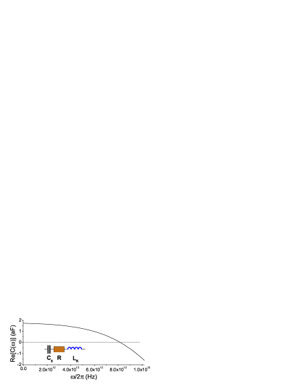
Our modeling approach also allows the study of the fundamental processes that control the AC properties of nanoelectronic devices. As an example, we show in Fig. 4 the real part of the total dynamic capacitance defined as with the total charge on the NT. At small frequencies is positive implying a capacitive-like behavior, but becomes inductive at THz as marked by the sign change. This characteristics is fundamentally different from that of traditional FETs which show only capacitive behavior. The origin of this unconventional behavior is the nanotube kinetic inductance. Indeed, we can model the NTFET as a classical RLC circuit as shown in Fig. 4 (inset), for which the dynamic capacitance where is the nanotube kinetic inductance and is the zero-frequency capacitance. This gives a transition to inductive behavior at , and from our numerical data for we extract nH for the 30 nm device. This value is consistent with that expected from simple arguments book .
In summary, we presented a new self-consistent approach for AC quantum transport and applied it to determine the high-frequency response of NTFETs. In the ON-state, the dynamic conductance shows divergent peaks, which are associated with the excitation of plasmons of the gated NTFET acting as resonant quantum cavity, whose mode spectrum can be tuned by varying the channel length. Our results suggest that low-dimensional systems with nanometer sized channels show potential for novel detectors and emitters of terahertz radiation. The approach can be applied to a broad range of nanoelectronic systems; it will be useful for the study of many time-dependent phenomena in low-dimensionality systems including phonon and defect scattering, ultrafast optical excitation, and entirely new operation modes of nanoelectronic devices.
We are indebted to M. Vaidyanathan and H. Guo for fruitful discussions. Sandia is a multiprogram laboratory operated by Sandia Corporation, a Lockheed Martin Co., for the United States Department of Energy under Contract No. DEAC01-94-AL85000.
References
- (1) S.V. Rotkin and S. Subramonev, Applied Physics of Carbon Nanotubes (Springer, New York, 2005); Y. Li et.al., Mater.Today 9, 18 (2006).
- (2) J. Appenzeller and D.J. Frank, Appl. Phys. Lett. 84, 1771 (2004); S. Li et.al., Nano Lett. 4, 753 (2004); L. Gomez-Rojas et.al., Nano Lett. 7, 2672 (2007); J. Chaste et.al., Nano Lett. 8, 525 (2008); Y. Lin et.al., Nano Lett. 9, 422 (2009).
- (3) Z. Zhong et.al., Nature Nanotechnol. 3, 201 (2008).
- (4) D. Bohm and E.P. Gross, Phys. Rev. 75, 1851 (1949).
- (5) H. Haug and A.-P. Jauho, Quantum Kinetics in Transport and Optics of Semiconductors (Springer, New York, 1998).
- (6) M.S. Purewal et.al., Phys. Rev. Lett. 98, 186808 (2007).
- (7) W. Zheng, Y. Wei, J. Wang, and H. Guo, Phys. Rev. B 61, 13121 (2000); Y. Zhu et.al., Phys. Rev. B 71, 075317 (2005); D. Hou et.al., Physica E 31, 191 (2006); B. Wang et.al., Phys. Rev. B 79, 155117 (2009).
- (8) A.-P. Jauho, N.S. Wingreen, and Y. Meir, Phys. Rev. B 50, 5528 (1994); G. Stefanucci and C.-O. Almbladh, Phys. Rev. B 69, 195318 (2004); V. Moldoveanu, V. Gudmundsson, and A. Manolescu, Phys. Rev. B 76, 085330 (2007).
- (9) B. Wang, J. Wang, and H. Guo, Phys. Rev. Lett. 82, 398 (1999).
- (10) F. Léonard and D.A. Stewart, Nanotechnology 17, 4699 (2006).
- (11) G.Y. Hu and R.F. O’Connell, J. Phys.: Cond. Matt. 2, 9381 (1990).
- (12) F. Léonard, The Physics of Carbon Nanotube Devices (William-Andrew, Norwich, 2008).